
Image not available
Illustrative purposes only

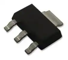
BSP75N
Power MOSFET, Enhancement Mode, N Channel, 60 V, 1.1 A, 0.55 ohm, SOT-223, Surface Mount
⚠️ Reference pricing provided. In case of supply shortages, we will connect you with our trusted procurement partners to ensure your project's continuity.
- Manufacturer: DIODES INC.
- Product type: Single MOSFETs
- Transistor Polarity:N Channel; Continuous Drain Current Id:1.1A; Drain Source Voltage Vds:60V; On Resistance Rds(on):0.5ohm; Rds(on) Test Voltage Vgs:10V; Threshold Voltage Vgs:2.1V; Pow
- MSL: -
- SVHC: Lead (25-Jun-2025)
- No. of Pins: 3Pins
- Channel Type: N Channel
- Product Range: -
- Qualification: -
- Power Dissipation: 1.5W
- Transistor Mounting: Surface Mount
- Rds(on) Test Voltage: 10V
- Transistor Case Style: SOT-223
- Drain Source Voltage Vds: 60V
- Operating Temperature Max: 150°C
- Continuous Drain Current Id: 1.1A
- Drain Source On State Resistance: 0.55ohm
- Gate Source Threshold Voltage Max: 2.1V
| Delivery and price | |
|---|---|
| Units per pack | 500 |
| Price | 0.703 € |
| Current stock | 10+ |
| Lead time | 30 days |
Datasheet

**BSP75N-13**

**60V SELF-PROTECTED LOW-SIDE IntelliFET MOSFET SWITCH**

**==> picture [18 x 6] intentionally omitted <==**

**----- Start of picture text -----**<br>
Green<br>**----- End of picture text -----**<br>


## **Product Summary**

- Continuous Drain-Source Voltage: VDS = 60V

- On-State Resistance: 500mΩ

- Max Nominal Load Current (VIN = 5V): 1.1A

- Min Nominal Load Current (VIN = 5V): 0.7A

- Clamping Energy: 550mJ

## **Description**

The BSP75N-13 is a self-protected, low-side IntelliFET[®] MOSFET. It features monolithic overtemperature, overcurrent, overvoltage (active clamp), and ESD protected logic-level functionality. It is intended as a general-purpose switch.

## **Applications**

- Especially suited for loads with high inrush current, such as lamps and motors

- All types of resistive, inductive, and capacitive loads in switching applications

- µC compatible power switches for 12V and 24V DC applications

- Replaces electromechanical relays and discrete circuits

- Linear mode capabilities—current-limiting protection circuitry is designed to deactivate at low VDS to not compromise the load current during normal operation. Maximum DC operating current is therefore determined by thermal capability of the

## **Features and Benefits**

- Short-Circuit Protection with Auto Restart

- Overvoltage Protection (Active Clamp)

- Thermal Shutdown with Auto Restart

- Overcurrent Protection

- Input Protection (ESD)

- Load-Dump Protection (Actively Protects Load)

- Logic-Level Input

- High Continuous Current Rating

- **Lead-Free Finish; RoHS Compliant (Note 1 & 2)**

- **Halogen and Antimony Free. “Green” Device (Note 3)**

- **For automotive applications requiring specific change control (i.e. parts qualified to AEC-Q100/101/104/200, PPAP capable, and manufactured in IATF 16949 certified facilities), please contact us or your local Diodes representative. https://www.diodes.com/quality/product-definitions/**

## **Mechanical Data**

   - Package: SOT223

   - Package Material: Molded Plastic, “Green” Molding Compound UL Flammability Classification Rating 94V-0

   - Moisture Sensitivity: Level 1 per J-STD-020

   - Terminals: Matte Tin Finish **e3**

   - Weight: 0.112 grams (Approximate)

- package/board combination rather than by protection circuitry,

- which does not compromise the product’s ability to self-protect at low VDS.

**==> picture [33 x 7] intentionally omitted <==**

**----- Start of picture text -----**<br>
SOT223<br>**----- End of picture text -----**<br>


**==> picture [37 x 8] intentionally omitted <==**

**----- Start of picture text -----**<br>
Top View<br>**----- End of picture text -----**<br>


**==> picture [37 x 16] intentionally omitted <==**

**----- Start of picture text -----**<br>
Top View<br>Pin Out<br>**----- End of picture text -----**<br>


## **Ordering Information** (Note 4)

|**Ordering Informationg Information Information** (Note 4)|**Ordering Informationg Information Information** (Note 4)|**Ordering Informationg Information Information** (Note 4)|**Ordering Informationg Information Information** (Note 4)|**Ordering Informationg Information Information** (Note 4)|**Ordering Informationg Information Information** (Note 4)|**Ordering Informationg Information Information** (Note 4)|
|---|---|---|---|---|---|---|
||||||||
|**Part Number**|**Package**|**Marking**|**Reel Size (inches)**|**Tape Width (mm)**|**Packing**||
||||||**Qty. **|**Carrier**|
|BSP75N-13|SOT223|BSP75N|13|12|4,000 Units|Reel|


- Notes: 1. EU Directive 2002/95/EC (RoHS), 2011/65/EU (RoHS 2) & 2015/863/EU (RoHS 3) compliant. All applicable RoHS exemptions applied.

   2. See https://www.diodes.com/quality/lead-free/ for more information about Diodes Incorporated’s definitions of Halogen- and Antimony-free, "Green" and Lead-free.

   3. Halogen- and Antimony-free "Green” products are defined as those which contain <900ppm bromine, <900ppm chlorine (<1500ppm total Br + Cl) and <1000ppm antimony compounds.

   4. For packaging details, go to our website at https://www.diodes.com/design/support/packaging/diodes-packaging/.

1 of 9 **www.diodes.com**

BSP75N-13 Document number: DS46251 Rev. 2 - 2

January 2024 © 2024 Copyright Diodes Incorporated. All Rights Reserved.

**BSP75N-13**

## **Marking Information**

BSP75N = Product Type Marking Code YWW = Date Code Marking Y or Y = Last Digit of Year (ex: 4 = 2024) WW or WW = Week Code (01 to 53)

## **Functional Block Diagram**

**==> picture [478 x 173] intentionally omitted <==**

**----- Start of picture text -----**<br>
Overvoltage<br>Protection<br>a<br>dv/dt<br>Limitation<br>Overtemperature<br>Human  Protection<br>Body ESD  i<br>Protection  Logic<br>Overcurrent<br>Protection<br>eee<br>**----- End of picture text -----**<br>


2 of 9 **www.diodes.com**

BSP75N-13 Document number: DS46251 Rev. 2 - 2

January 2024 © 2024 Copyright Diodes Incorporated. All Rights Reserved.

**BSP75N-13**

**Absolute Maximum Ratings** (@TA = +25°C, unless otherwise specified.)

**==> picture [518 x 241] intentionally omitted <==**

**----- Start of picture text -----**<br>
|||||||
|---|---|---|---|---|---|
|OG|Parameter|Symbol|Value|Unit|
|CG|Continuous Drain-Source Voltage|VDS|60|V|
|pf|Drain-Source Voltage for Short-Circuit Protection, VIN = 5V|VDS(SC)|36|V|
|Ce|Drain-Source Voltage for Short-Circuit Protection, VIN = 10V|VDS(SC)|CO|20|V|
|CG|Continuous Input Voltage|VIN|-0.2 to 10|V|
|Ce|Peak Input Voltage|VIN|CO|-0.2 to 20|V|
|CG|Operating Temperature Range|TJ|-40 to +150|°C|
|Ce|Storage Temperature Range|TSTG|CO|-55 to +150|°C|
|OG|Power Dissipation at TA|= +25°C (Note 5)|PD|1.5|W|
|CG|Power Dissipation at TA|= +25°C (Note 6)|PD|0.6|W|
|Ce|Continuous Drain Current @ VIN = 10V, TA = +25°C (Note 5)|ID|CO|1.3|A|
|CG|Continuous Drain Current @ VIN = 5V, TA = +25°C (Note 5)|ID|1.1|A|
|GG|Continuous Drain Current @ VIN = 5V, TA = +25°C (Note 6)|ID|0.7|A|
|CG|Continuous Source Current (Body Diode)|(Note 5)|IS|2.0|A|
|CG|Pulsed Source Current (Body Diode)|(Note 7)|IS|3.3|A|
|Unclamped Single Pulse Inductive Energy|EAS|550|mJ|
|Ce|Load Dump Protection|VLOAD_DUMP|Ge|80|V|
|Electrostatic Discharge (Human Body Model)|VESD|4000|V|
|Ce|DIN Humidity Category, DIN 40 040|—|Ge|E|—|
|IEC Climatic Category, DIN IEC 68-1|—|40/150/56|—|

**----- End of picture text -----**<br>


## **Thermal Resistance**

**==> picture [491 x 45] intentionally omitted <==**

**----- Start of picture text -----**<br>
|||||
|---|---|---|---|
|Parameter|Symbol|Value|Unit|
|Junction to Ambient (Note 5)|RθJA|83|°C/W|
|Junction to Ambient (Note 7)|RθJA|45|°C/W|
|Junction to Ambient (Note 6)|RθJA|208|°C/W|

**----- End of picture text -----**<br>


Notes: 5. For a device surface-mounted on 25mm x 25mm x 1.6mm FR-4 board with a high coverage of single-sided 2oz weight copper. Allocation of 6cm[2] coppe 33% to source tab and 66% to drain pin with source tab and drain pin electrically isolated.

6. For a device surface-mounted on FR-4 board with the minimum copper required for electrical connections.

7. For a device surface-mounted on FR-4 board as (a) and measured at t ≤ 10s.

3 of 9 **www.diodes.com**

BSP75N-13 Document number: DS46251 Rev. 2 - 2

January 2024 © 2024 Copyright Diodes Incorporated. All Rights Reserved.

**BSP75N-13**

**Electrical Characteristics** (@TA = +25°C, unless otherwise specified.)

|**Electrical Characteristics** (@TA = +25°C, unless otherwise specified.)A = +25°C, unless otherwise specified.)= +25°C, unless otherwise specified.)|**Electrical Characteristics** (@TA = +25°C, unless otherwise specified.)A = +25°C, unless otherwise specified.)= +25°C, unless otherwise specified.)|**Electrical Characteristics** (@TA = +25°C, unless otherwise specified.)A = +25°C, unless otherwise specified.)= +25°C, unless otherwise specified.)|**Electrical Characteristics** (@TA = +25°C, unless otherwise specified.)A = +25°C, unless otherwise specified.)= +25°C, unless otherwise specified.)|**Electrical Characteristics** (@TA = +25°C, unless otherwise specified.)A = +25°C, unless otherwise specified.)= +25°C, unless otherwise specified.)|**Electrical Characteristics** (@TA = +25°C, unless otherwise specified.)A = +25°C, unless otherwise specified.)= +25°C, unless otherwise specified.)|**Electrical Characteristics** (@TA = +25°C, unless otherwise specified.)A = +25°C, unless otherwise specified.)= +25°C, unless otherwise specified.)|**Electrical Characteristics** (@TA = +25°C, unless otherwise specified.)A = +25°C, unless otherwise specified.)= +25°C, unless otherwise specified.)|
|---|---|---|---|---|---|---|---|
|||||||||
|**Characteristic**<br>~~po~~|**Symbol**<br>~~po~~<br>~~ee~~|**Min**<br>~~po~~<br>~~ee~~|**Typ**<br>~~po~~<br>~~ee~~|**Max**<br>~~po~~<br>~~ee~~|**Unit**<br>~~po~~<br>~~ee~~||**Conditions**<br>~~po~~|
|**Static Characteristics**<br>~~es~~<br>~~eeeeeeee~~||||||||
|Drain-Source ClampVoltage<br>~~es~~|VDS(AZ)<br>~~es~~<br>~~ee~~<br>~~ee~~|60<br>~~es~~<br>~~ee~~<br>~~ee~~|70<br>~~es~~<br>~~ee~~<br>~~ee~~|75<br>~~es~~<br>~~ee~~<br>~~ee~~|V<br>~~es~~<br>~~ee~~||ID= 10mA<br>~~es~~|
|Off-State Drain Current<br>~~ee~~|IDSS<br>~~ee~~<br>~~ee~~<br>~~ee~~|—<br>~~ee ~~<br>~~ee~~<br>~~ee~~|0.1<br> ~~ee ~~<br>~~ee~~<br>~~ee~~|3<br> ~~ee ~~<br>~~ee~~<br>~~ee~~|µA<br> ~~ee~~<br>~~ee~~||VDS= 12V,VIN= 0V<br>~~ee~~|
|Off-State Drain Current<br>~~ee~~|IDSS<br>~~ee~~<br>~~ee~~<br>~~ee~~|—<br>~~ee~~<br>~~ee~~<br>~~ee~~|3<br>~~ee~~<br>~~ee~~<br>~~ee~~|15<br>~~ee~~<br>~~ee~~<br>~~ee~~|µA<br>~~ee~~||VDS= 32V,VIN= 0V<br>~~ee~~|
|Input Threshold Voltage (Note 8)<br>~~ee~~|VIN(TH)<br>~~ee~~<br>~~ee~~<br>~~ee~~|1<br>~~ee~~<br>~~ee~~<br>~~ee~~|2.1<br>~~ee ~~<br>~~ee~~<br>~~ee~~|—<br> ~~ee~~<br>~~ee~~<br>~~ee~~|V<br>~~ee~~||VDS= VGS,ID= 1mA<br>~~ee~~|
|Input Current<br>~~ee~~|IIN<br>~~ee~~<br>~~ee~~<br>~~ee~~|—<br>~~ee~~<br>~~ee~~<br>~~ee~~|0.7<br>~~ee~~<br>~~ee~~<br>~~ee~~|1.2<br>~~ee~~<br>~~ee~~<br>~~ee~~|mA<br>~~ee~~<br>~~ee~~||VIN= 5V<br>~~ee~~|
|Input Current<br>~~es~~|IIN<br>~~ee ~~<br>~~es~~<br>~~ee~~|—<br> ~~ee~~<br>~~es~~<br>~~ee~~|1.5<br>~~ee ~~<br>~~es~~<br>~~ee~~|2.7<br> ~~ee~~<br>~~es~~<br>~~ee~~|mA<br>~~es~~<br>~~ee~~||VIN= 7V<br>~~es~~|
|Input Current<br>~~es~~|IIN<br>~~es~~<br>~~ee~~|—<br>~~es~~<br>~~ee~~|4<br>~~es~~<br>~~ee~~|7<br>~~es~~<br>~~ee~~|mA<br>~~es~~<br>~~ee~~||VIN= 10V<br>~~es~~|
|Static Drain-Source On-State Resistance<br>~~eee~~|RDS(ON)<br>~~ee ~~<br>~~eee~~|—<br> ~~ee ~~<br>~~eee~~|520<br> ~~ee ~~<br>~~eee~~|675<br> ~~ee ~~<br>~~eee~~|mΩ<br> ~~ee~~<br>~~eee~~||VIN= 5V,ID= 0.7A<br>~~eee~~|
|Static Drain-Source On-State Resistance<br>~~eee~~|RDS(ON)<br>~~eee~~|—<br>~~eee~~|385<br>~~eee~~|550<br>~~eee~~<br>~~ee~~|mΩ<br>~~eee~~<br>~~ee~~||VIN= 10V,ID= 0.7A<br>~~eee~~|
|Current Limit(Note 9)<br>~~ee~~|ID(LIM)<br>~~ee~~|0.7<br>~~ee~~|1.0<br>~~ee~~|1.5<br>~~ee~~<br>~~ee~~|A<br>~~ee~~<br>~~ee~~||VIN= 5V,VDS> 5V<br>~~ee~~|
|Current Limit(Note 9)<br>~~ee~~|ID(LIM)<br>~~ee~~|1<br>~~ee~~|1.8<br>~~ee~~|2.3<br>~~ee~~<br>~~ee~~|A<br>~~ee~~<br>~~ee~~||VIN= 10V,VDS> 5V<br>~~ee~~|
|**Dynamic Characteristics**<br>~~ee~~<br>~~pe~~<br>~~SeeG~~||||||||
|Turn-On Time (VINto 90% ID)<br>~~Se~~|tON<br>~~eG~~<br>~~Oe~~|—<br>~~eG~~<br>~~Oe~~|3<br>~~eG~~<br>~~Oe~~|—<br>~~eG~~|μs|RL= 22Ω, VIN= 0V to 10V<br>VDD= 12V||
|Turn-Off Time (VIN to 90% ID)<br>~~Se ~~<br>~~Se~~|tOFF<br> ~~eG~~<br>~~Se~~<br>~~Oe~~|—<br>~~eG~~<br>~~Se~~<br>~~Oe~~<br>~~ee~~|13<br>~~eG~~<br>~~Se~~<br>~~Oe~~<br>~~ee~~|—<br>~~eG~~<br>~~Se~~|μs<br>~~Se~~|RL= 22Ω, VIN= 10V to 0V<br>VDD= 12V<br>~~Se~~||
|Slew Rate On (70% to 50% VDD)<br>~~ee~~|-dvDS/dtON<br>~~Oe~~<br>~~ee~~|—<br>~~Oe~~<br>~~ee~~<br>~~ee~~|8<br>~~Oe~~<br>~~ee~~<br>~~ee~~<br>~~De~~|—<br>~~ee~~<br>~~De~~|V/μs<br>~~ee~~|RL= 22Ω, VIN= 0V to 10V<br>VDD= 12V<br>~~ee~~||
|Slew Rate Off (50% to 70% VDD)<br>~~Pe~~|dvDS/dtON<br>~~Pe~~|—<br>~~ee~~<br>~~Pe~~|3.2<br>~~ee~~<br>~~Pe~~<br>~~De~~|—<br>~~Pe~~<br>~~De~~|V/μs<br>~~Pe~~|RL= 22Ω, VIN= 10V to 0V<br>VDD= 12V<br>~~Pe~~||
|**Protection Functions(Note 10)**<br>~~De~~<br>~~es ee~~||||||||
|Minimum Input Voltage for Overtemperature<br>Protection<br>~~ee~~<br>~~Se~~|VPROT<br>~~ee~~<br>~~es ee~~<br>|4.5<br>~~ee~~<br>~~ee~~<br>|—<br>~~ee~~<br>~~ee~~<br>|—<br>~~ee~~<br>~~ee~~<br>|V<br>~~ee~~<br>~~ee~~<br>|—<br>~~ee~~<br>||
|Thermal Overload TripTemperature<br>~~ee~~<br>~~Se~~|TJT<br>~~es ee~~<br>~~ee~~<br>|+150<br>~~ee~~<br>~~ee~~<br>|+175<br>~~ee~~<br>~~ee~~<br>|—<br>~~ee~~<br>~~ee~~<br>|°C<br>~~ee~~<br>~~ee~~<br>|—<br>~~ee~~<br>||
|Thermal Hysteresis<br>~~ee~~<br>~~Se~~|—<br>~~ee~~<br>|—<br>~~ee~~<br>|+1<br>~~ee~~<br>|—<br>~~ee~~<br>~~ee~~<br>|°C<br>~~ee~~<br>~~ee~~<br>|—<br>~~ee~~<br>||
|Unclamped Single Pulse Inductive Energy<br>TJ= +25°C<br>~~Se ~~|EAS<br> ~~GO~~|550<br>~~GO~~|—<br>~~GO~~|—<br>~~ee~~<br>~~GO~~|mJ<br>~~ee~~<br>~~GO~~|ID(ISO)= 0.7A, VDD= 32V<br>~~GO~~||
|Unclamped Single Pulse Inductive Energy<br>TJ= +150°C<br>~~Se ~~<br>~~GC~~|EAS<br> <br>~~GC~~|200<br><br>~~GC~~<br>~~ee~~|—<br><br>~~GC~~<br>~~ee~~|—<br>~~ee~~<br><br>~~GC~~<br>~~ee~~|mJ<br>~~ee~~<br><br>~~GC~~<br>~~ee~~|ID(ISO)= 0.7A, VDD= 32V<br><br>~~GC~~||
|**Inverse Diode**<br>~~ee~~<br>~~ee~~||||||||
|Source-Drain Voltage<br>~~ee~~|VSD<br>~~ee~~|—<br>~~ee~~<br>~~ee~~|—<br>~~ee~~<br>~~ee~~|1<br>~~ee~~<br>~~ee~~|V<br>~~ee~~<br>~~ee~~|VIN= 0V,-ID= 1.4A<br>~~ee~~||


4 of 9 **www.diodes.com**

BSP75N-13 Document number: DS46251 Rev. 2 - 2

January 2024 © 2024 Copyright Diodes Incorporated. All Rights Reserved.

**BSP75N-13**

## **Application Information**

The current-limit protection circuitry is designed to deactivate at low VDS to prevent the load current from being unnecessarily restricted during normal operation. The design max DC operating current is therefore determined by the thermal capability of the package/board combination rather than by the protection circuitry (see _Typical Characteristics_ graphs). This does not compromise the products ability to self-protect at low VDS.

The overtemperature protection circuit trips at a minimum of +150°C, so the available package dissipation reduces as the maximum required ambient temperature increases. This leads to the following maximum recommended continuous operating currents.

## **Minimum Copper Area Characteristics**

For minimum copper condition as described in Note 6.

|**Max Ambient Temperature TA**|**Maximum Continuous Current**|**Maximum Continuous Current**|
|---|---|---|
||**VIN = 5V**|**VIN = 10V**|
|+25°C|720mA|840mA|
|+70°C|575mA|670mA|
|+85°C|520mA|605mA|
|+125°C|320mA|375mA|


**==> picture [407 x 204] intentionally omitted <==**

**----- Start of picture text -----**<br>
RDS(ON)<br>_ Limited  a S06 See Note 6 » Minimum Copper<br>1 a. SD =<br>o B04<br>c oc a<br>= See, =]<br>So 1s a<br>° 100ms ’ Oo<br>TA=25°C<br>®0tom| Sse Pulse | 10ms /f 502<br>¥<br>=Limit of DC Self Protection -40°C to 150°C a.<br>im ay 0.0<br>Vos1 [Drain-Source] 10 [Voltage] [(V)] 100 S020 40Temperature«G0 80 (°C)«100 120 140<br>safe Operating Area Derating Curve<br>200 TA = 25°C “ _ T Single A = 25°C  Pulse<br>**----- End of picture text -----**<br>


5 of 9 **www.diodes.com**

BSP75N-13 Document number: DS46251 Rev. 2 - 2

January 2024 © 2024 Copyright Diodes Incorporated. All Rights Reserved.

**BSP75N-13**

## **Large Copper Area Characteristics**

For large copper area as described in Note 5.

|**Max Ambient Temperature TA**|**Maximum Continuous Current**|**Maximum Continuous Current**|
|---|---|---|
||**VIN = 5V**|**VIN = 10V**|
|+25°C|1140mA|1325mA|
|+70°C|915mA|1060mA|
|+85°C|825mA|955mA|
|+125°C|510mA|590mA|


**==> picture [309 x 90] intentionally omitted <==**

**----- Start of picture text -----**<br>
RDS(ON)<br>Limited<br>See Note 5<br>00 “ai 810<br>1s A a8<br>100ms i O06<br>T Single A = 25°C  Pulse 10ms } te<br>**----- End of picture text -----**<br>


**==> picture [367 x 22] intentionally omitted <==**

**----- Start of picture text -----**<br>
TA = 25°C _ T Single A = 25°C  Pulse<br>**----- End of picture text -----**<br>


6 of 9 **www.diodes.com**

BSP75N-13 Document number: DS46251 Rev. 2 - 2

January 2024 © 2024 Copyright Diodes Incorporated. All Rights Reserved.

**BSP75N-13**

## **Typical Characteristics**

**==> picture [384 x 188] intentionally omitted <==**

**----- Start of picture text -----**<br>
PyAR oL_ LETT TTT TTT TTT I<br>o12 3 4 5 6 7 8 9 1011 50 -25 O 25 50 75 100 125<br>Vs Drain-Source Voltage (V) T, Junction Temperature (°C)<br>Typical Output Characteristic On-State Resistance vs Temperature<br>=~ 2000 14<br>GL ttt yt yt po<br>® 1500 PP 1.2 a ee<br>5 en eee lols<br>8 ap Hf} FS gs EL [TNT]<br>oeec reE<br>Ft | | | tdTS 2 068 ps ta ON<br>o0LETTETT TT | | git Pt<br>DS(ON)<br>R<br>IN(TH)<br>V<br>DS(ON)<br>R<br>**----- End of picture text -----**<br>


7 of 9 **www.diodes.com**

BSP75N-13 Document number: DS46251 Rev. 2 - 2

January 2024

© 2024 Copyright Diodes Incorporated. All Rights Reserved.

**BSP75N-13**

## **Package Outline Dimensions**

Please see http://www.diodes.com/package-outlines.html for the latest version.

## **SOT223**

**==> picture [417 x 218] intentionally omitted <==**

**----- Start of picture text -----**<br>
D<br>= b1 Q<br>C<br>SOT223<br>Dim  Min  Max  Typ<br>A 1.55 1.65 1.60<br>|] E E1 — A1 0.010 0.15 0.05<br>b 0.60 0.80 0.70<br>b1 2.90 3.10 3.00<br>Gauge<br>Plane C 0.20 0.30 0.25<br>0.25 D 6.45 6.55 6.50<br>Seating L E 3.45 3.55 3.50<br>Plane =See<br>E1 6.90 7.10 7.00<br>e1 b e -  -  4.60<br>atpote e s [|] ium a e1 -  -  2.30<br>L 0.85 1.05 0.95<br>Q 0.84  0.94  0.89<br>A A1 7° All Dimensions in mm<br>0°-10°<br>7°<br>**----- End of picture text -----**<br>


## **Suggested Pad Layout**

Please see http://www.diodes.com/package-outlines.html for the latest version.

## **SOT223**

**==> picture [154 x 148] intentionally omitted <==**

**----- Start of picture text -----**<br>
X1<br>Y1<br>I<br>C1 Y2<br>Y<br>goo. X C<br>**----- End of picture text -----**<br>


**==> picture [106 x 75] intentionally omitted <==**

**----- Start of picture text -----**<br>
Dimensions Value (in mm)<br>C 2.30<br>C1  6.40<br>X  1.20<br>X1  3.30<br>Y  1.60<br>Y1  1.60<br>Y2  8.00<br>**----- End of picture text -----**<br>


8 of 9 **www.diodes.com**

BSP75N-13 Document number: DS46251 Rev. 2 - 2

January 2024 © 2024 Copyright Diodes Incorporated. All Rights Reserved.

**BSP75N-13**

## **IMPORTANT NOTICE**

1. DIODES INCORPORATED (Diodes) AND ITS SUBSIDIARIES MAKE NO WARRANTY OF ANY KIND, EXPRESS OR IMPLIED, WITH REGARDS TO ANY INFORMATION CONTAINED IN THIS DOCUMENT, INCLUDING, BUT NOT LIMITED TO, THE IMPLIED WARRANTIES OF MERCHANTABILITY, FITNESS FOR A PARTICULAR PURPOSE OR NON-INFRINGEMENT OF THIRD PARTY INTELLECTUAL PROPERTY RIGHTS (AND THEIR EQUIVALENTS UNDER THE LAWS OF ANY JURISDICTION).

2. The Information contained herein is for informational purpose only and is provided only to illustrate the operation of Diodes’ products described herein and application examples. Diodes does not assume any liability arising out of the application or use of this document or any product described herein. This document is intended for skilled and technically trained engineering customers and users who design with Diodes’ products. Diodes’ products may be used to facilitate safety-related applications; however, in all instances customers and users are responsible for (a) selecting the appropriate Diodes products for their applications, (b) evaluating the suitability of Diodes’ products for their intended applications, (c) ensuring their applications, which incorporate Diodes’ products, comply the applicable legal and regulatory requirements as well as safety and functional-safety related standards, and (d) ensuring they design with appropriate safeguards (including testing, validation, quality control techniques, redundancy, malfunction prevention, and appropriate treatment for aging degradation) to minimize the risks associated with their applications.

3. Diodes assumes no liability for any application-related information, support, assistance or feedback that may be provided by Diodes from time to time. Any customer or user of this document or products described herein will assume all risks and liabilities associated with such use, and will hold Diodes and all companies whose products are represented herein or on Diodes’ websites, harmless against all damages and liabilities.

4. Products described herein may be covered by one or more United States, international or foreign patents and pending patent applications. Product names and markings noted herein may also be covered by one or more United States, international or foreign trademarks and trademark applications. Diodes does not convey any license under any of its intellectual property rights or the rights of any third parties (including third parties whose products and services may be described in this document or on Diodes’ website) under this document.

5. Diodes’ products are provided subject to Diodes’ Standard Terms and Conditions of Sale (https://www.diodes.com/about/company/terms-and-conditions/terms-and-conditions-of-sales/) or other applicable terms. This document does not alter or expand the applicable warranties provided by Diodes. Diodes does not warrant or accept any liability whatsoever in respect of any products purchased through unauthorized sales channel.

6. Diodes’ products and technology may not be used for or incorporated into any products or systems whose manufacture, use or sale is prohibited under any applicable laws and regulations. Should customers or users use Diodes’ products in contravention of any applicable laws or regulations, or for any unintended or unauthorized application, customers and users will (a) be solely responsible for any damages, losses or penalties arising in connection therewith or as a result thereof, and (b) indemnify and hold Diodes and its representatives and agents harmless against any and all claims, damages, expenses, and attorney fees arising out of, directly or indirectly, any claim relating to any noncompliance with the applicable laws and regulations, as well as any unintended or unauthorized application.

7. While efforts have been made to ensure the information contained in this document is accurate, complete and current, it may contain technical inaccuracies, omissions and typographical errors. Diodes does not warrant that information contained in this document is error-free and Diodes is under no obligation to update or otherwise correct this information. Notwithstanding the foregoing, Diodes reserves the right to make modifications, enhancements, improvements, corrections or other changes without further notice to this document and any product described herein. This document is written in English but may be translated into multiple languages for reference. Only the English version of this document is the final and determinative format released by Diodes.

8. Any unauthorized copying, modification, distribution, transmission, display or other use of this document (or any portion hereof) is prohibited. Diodes assumes no responsibility for any losses incurred by the customers or users or any third parties arising from any such unauthorized use.

9. This Notice may be periodically updated with the most recent version available at https://www.diodes.com/about/company/terms-andconditions/important-notice

The Diodes logo is a registered trademark of Diodes Incorporated in the United States and other countries. All other trademarks are the property of their respective owners. © 2024 Diodes Incorporated. All Rights Reserved.

**www.diodes.com**

9 of 9 **www.diodes.com**

BSP75N-13 Document number: DS46251 Rev. 2 - 2

January 2024 © 2024 Copyright Diodes Incorporated. All Rights Reserved.
Updated at June 5, 2026
About Novapart
Novapart is a B2B electronic component broker specialising in stock shortages and cost reduction. We source hard-to-find parts and identify compliant alternatives across a catalogue of 410,000+ components from 500+ manufacturers.
Learn more →Stock Shortage Specialist
When a component is unavailable, discontinued or has an unacceptable lead time, we tap into our network of vetted European and Asian distributors to source what you need — without compromising on quality or traceability.
Request a quote →Compliant Alternatives
We identify pin-to-pin, electrically equivalent substitutes that meet the same certifications (RoHS, AEC-Q100, REACH) as your original specification — validated against datasheets, not just part numbers. Often at a lower cost.
BOM Analysis service →