
Image not available
Illustrative purposes only

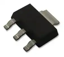
BSP75G
Power MOSFET, Enhancement Mode, N Channel, 60 V, 1.4 A, 0.55 ohm, SOT-223, Surface Mount
⚠️ Reference pricing provided. In case of supply shortages, we will connect you with our trusted procurement partners to ensure your project's continuity.
- Manufacturer: DIODES INC.
- Product type: Single MOSFETs
- SVHC: Lead (25-Jun-2025)
- No. of Pins: 3Pins
- Channel Type: N Channel
- Product Range: -
- Qualification: -
- Power Dissipation: 2.5W
- Transistor Mounting: Surface Mount
- Rds(on) Test Voltage: 10V
- Transistor Case Style: SOT-223
- Drain Source Voltage Vds: 60V
- Operating Temperature Max: 150°C
- Continuous Drain Current Id: 1.4A
- Drain Source On State Resistance: 0.55ohm
- Gate Source Threshold Voltage Max: 2.1V
| Delivery and price | |
|---|---|
| Units per pack | 3000 |
| Price | 0.545 € |
| Current stock | 10+ |
| Lead time | 30 days |
Datasheet

**==> picture [108 x 43] intentionally omitted <==**

## **BSP75G 60V N-channel self-protected enhancement mode IntelliFET[TM] MOSFET**

## **Summary**

S Continuous drain source voltage VDS=60V On-state resistance 550m Ω Nominal load current 1.6A D D Clamping energy 550mJ SOT223 IN

## **Description**

Self-protected low side MOSFET. Monolithic over temperature, over current, over voltage (active clamp) and ESD protected logic level power MOSFET intended as a general purpose switch.

## **Features**

- High continuous current rating

- Logic Level Input

- Input protection (ESD)

- Thermal shutdown with auto restart

- Over load protection

## **Note:**

Drain tab may be electrically isolated provided electrical connection is made to the drain pin, and thermal connection to the drain tab is maintained to ensure thermal performance.

- Short circuit protection with auto restart

- Over voltage protection (active clamp)

- Load dump protection (actively protects load)

## **Applications**

- Especially suited for loads with a high inrush current such as lamps and motors

- All types of resistive, inductive and capacitive loads in switching applications

- μ C compatible power switch for 12V and 24V DC applications and for 42V powernet

- Automotive rated

- Replaces electromechanical relays and discrete circuits

## **Functional block diagram**

**==> picture [293 x 164] intentionally omitted <==**

**----- Start of picture text -----**<br>
D<br>Over voltage<br>protection<br>dV/dt<br>IN limitation<br>Over current<br>Human protection<br>body ESD<br>protection Logic<br>Over temperature<br>protection<br>S<br>**----- End of picture text -----**<br>


**Issue 2 - April 2005** © Zetex Semiconductors plc 2005

**1**

**www.zetex.com**

## **BSP75G**

## **Absolute maximum ratings**

|**Parameter**|**Symbol**|**Limit**|**Unit**|
|---|---|---|---|
|Continuous drain-source voltage|VDS|60|V|
|Drain-source voltage for short circuit protection|VDS(SC)|36|V|
|Continuous input voltage|VIN|-0.2 ... +10|V|
|Peak input voltage|VIN|-0.2 ... +20|V|
|Operating temperature range|Tj,|-40 to +150|°C|
|Storage temperature range|Tstg|-55 to +150|°C|
|Power dissipation at TA=25°C*|PD|2.5|W|
|Continuous drain current @ VIN=10V; TA=25°C*|ID|1.6|A|
|Continuous drain current @ VIN=5V; TA=25°C*|ID|1.4|A|
|Pulsed drain current @ VIN=10V|IDM|5|A|
|Continuous source current (body diode)*|IS|3|A|
|Pulsed source current (body diode)|IS|5|A|
|Unclamped single pulse inductive energy|EAS|550|mJ|
|Load dump protection|VLoadDump|80|V|
|Electrostatic discharge (human body model)|VESD|4000|V|
|DIN humidity category, DIN 40 040||E||
|IEC climatic category, DIN IEC 68-1||40/150/56||


## **Thermal resistance**

|**Parameter**|**Symbol**|**Value**|**Unit**|
|---|---|---|---|
|Junction to Ambient*|RJA|50|°C/W|
|Junction to Ambient†|RJA|34|°C/W|


## **NOTES:**

* For a device surface mounted on 37mm x 37mm x 1.6mm FR4 board with a high coverage of single sided 2oz weight copper.

- For a device surface mounted on FR4 board and measured at t<=10s.

**Issue 2 - April 2005** © Zetex Semiconductors plc 2005

**2**

**www.zetex.com**

**BSP75G**

## **Characteristics**

**==> picture [419 x 332] intentionally omitted <==**

**----- Start of picture text -----**<br>
2.00<br>RDS(on)<br>Limited 1.75<br>1<br>1.50<br>1.25<br>DC<br>1s 1.00<br>100m<br>Single Pulse 100ms 0.75<br>Tamb=25°C 10ms 0.50<br>Limit of DC Self Protection 0.25<br>10m<br>0.00<br>1 10 100 0 20 40 60 80 100 120 140 160<br>VDS  Drain-Source Voltage (V)  Temperature (°C)<br>Safe Operating Area Derating Curve<br>60 Tamb=25°C Single Pulse<br>50 Tamb=25°C<br>100<br>40<br>D=0.5<br>30<br>10<br>20<br>D=0.2 Single Pulse<br>10 D=0.05<br>D=0.1<br>0 1<br>100µ 1m 10m 100m 1 10 100 1k 100µ 1m 10m 100m 1 10 100 1k<br>Pulse Width (s) Pulse Width (s)<br>Transient Thermal Impedance Pulse Power Dissipation<br>  Drain Current (A)<br>ID<br> Max Power Dissipation (W)<br> Maximum Power (W)<br>Thermal Resistance (°C/W)<br>**----- End of picture text -----**<br>


**Issue 2 - April 2005** © Zetex Semiconductors plc 2005

**3**

**www.zetex.com**

**BSP75G**

## **Electrical characteristics (at Tamb = 25°C unless otherwise stated)**

|**Parameter**|**Symbol**|**Min**|**Typ**|**Max**|**Unit**|**Conditions**|
|---|---|---|---|---|---|---|
|**Static Characteristics**|||||||
|Drain-source clamp voltage|VDS(AZ)|60|70|75|V|ID=10mA|
|Off state drain current|IDSS||0.1|3|μA|VDS=12V,<br>VIN=0V|
|Off state drain current|IDSS||3|15|μA|VDS=32V,<br>VIN=0V|
|Input threshold voltage*|VIN(th)|1|2.1||V|VDS=VGS,<br>ID=1mA|
|Input current|IIN||0.7|1.2|mA|VIN=+5V|
|Input current|IIN||1.5|2.7|mA|VIN=+7V|
|Input current|IIN||4|7|mA|VIN=+10V|
|Static drain-source on-state<br>resistance|RDS(on)||520|675|mΩ|VIN=5V,<br>ID=0.7A|
|Static drain-source on-state<br>resistance|RDS(on)||385|550|mΩ|VIN=10V,<br>ID=0.7A|
|Current limit†|ID(LIM)|0.7|1.1|1.75|A|VIN=5V,<br>VDS>5V|
|Current limit†|ID(LIM)|2|3|4|A|VIN=10V,<br>VDS>5V|
|**Dynamic characteristics**|||||||
|Turn-on time (VINto 90% ID)|ton||2.2|10|μs|RL=22Ω,<br>VIN=0 to 10V,<br>VDD=12V|
|Turn-off time (VINto 90% ID)|toff||13|20|μs|RL=22Ω,<br>VIN=10V to<br>0V, VDD=12V|
|Slew rate on (70 to 50% VDD)|-dVDS/dton||10|20|V/μs|RL=22Ω,<br>VIN=0 to 10V,<br>VDD=12V|
|Slew rate off (50 to 70% VDD)|dVDS/dton||3.2|10|V/μs|RL=22Ω,<br>VIN=10V to 0V,<br>VDD=12V|


**Issue 2 - April 2005** © Zetex Semiconductors plc 2005

**4**

**www.zetex.com**

## **BSP75G**

**Electrical characteristics (at Tamb = 25°C unless otherwise stated) (Continued)**

|**Parameter**|**Symbol**|**Min**|**Typ**|**Max**|**Unit**|**Conditions**|
|---|---|---|---|---|---|---|
|**Protection Functions‡**|||||||
|Required input voltage for<br>over temperature protection|VPROT|4.5|||V||
|Thermal Overload trip<br>temperature|TJT|150|175||°C||
|Thermal hysteresis|||10||°C||
|Unclamped single pulse<br>inductive energy<br>Tj=25°C|EAS|550|||mJ|ID(ISO)=0.7A,<br>VDD=32V|
|Unclamped single pulse<br>inductive energy<br>Tj=150°C|EAS|200|||mJ|ID(ISO)=0.7A,<br>VDD=32V|
|**Inverse Diode**|||||||
|Source drain voltage|VSD||||1|VIN=0V,<br>-ID=1.4A|


## **NOTES:**

- Protection features may operate outside spec for VIN<4.5V.

† The drain current is limited to a reduced value when Vds exceeds a safe level.

‡ Integrated protection functions are designed to prevent IC destruction under fault conditions described in the datasheet. Fault conditions are considered as "outside" normal operating range. Protection functions are not designed for continuous, repetitive operation.

**Issue 2 - April 2005** © Zetex Semiconductors plc 2005

**5**

**www.zetex.com**

**BSP75G**

## **Typical characteristics**

**==> picture [426 x 487] intentionally omitted <==**

**----- Start of picture text -----**<br>
1000<br>5 T = 25°C<br>800<br>4 VIN<br>10V 600<br>3 9V<br>8V<br>2 7V 400<br>6V<br>1 4V5V 200 VIDIN = 0.7A = 10V<br>0 0<br>0 2 4 6 8 10 12 -50 -25 0 25 50 75 100 125 150<br>VDS  Drain-Source Voltage (V) Tj  Junction Temperature (°C)<br>Typical Output Characteristic Typical On-state Resistance<br>1000 2.0<br>RDS(ON)<br>800 VIN = 10V<br>1.5 ID = 0.7A<br>600<br>1.0<br>400<br>200 VIDIN = 0.7A = 5V 0.5 VVIDGS(th)GS = 1mA = VDS<br>0 0.0<br>-50 -25 0 25 50 75 100 125 150 -50 0 50 100 150<br>Tj  Junction Temperature (°C) Tj  Junction Temperature (°C)<br>Typical On-state Resistance Typical Input Threshold Voltage<br>2000 4<br>T = 25°C T = 25°C<br>1500 ID = 0.7A 3 VDS=10V<br>1000 2<br>500 1<br>0 0<br>0 2 4 6 8 10 0 2 4 6 8 10<br>VIN  Input Voltage (V) VIN  Input Voltage (V)<br>Typical On-state Resistance Source-Drain Diode Forward Voltage<br>)<br>Ω<br>  Drain Current (A)  On-Resistance (<br>ID<br>DS(on)<br>R<br>)<br>GS(th)<br>Ω  and V<br>DS(on)<br> On-Resistance (<br>DS(on)<br>R<br>Normalised R<br>)<br>Ω<br> On-Resistance (<br>  Drain Current (A)<br>ID<br>DS(on)<br>R<br>**----- End of picture text -----**<br>


**Issue 2 - April 2005** © Zetex Semiconductors plc 2005

**6**

**www.zetex.com**

**BSP75G**

**==> picture [455 x 301] intentionally omitted <==**

Intentionally left blank

**Issue 2 - April 2005** © Zetex Semiconductors plc 2005

**7**

**www.zetex.com**

**BSP75G**

## **Packaging details**

**==> picture [356 x 467] intentionally omitted <==**

|**Europe**|**Americas**|**Asia Pacific**|**Corporate Headquarters**|
|---|---|---|---|
|Zetex GmbH|Zetex Inc|Zetex (Asia Ltd)|Zetex Semiconductors plc|
|Streitfeldstraße 19|700 Veterans Memorial Highway|3701-04 Metroplaza Tower 1|Zetex Technology Park, Chadderton|
|D-81673 München|Hauppauge, NY 11788|Hing Fong Road, Kwai Fong|Oldham, OL9 9LL|
|Germany|USA|Hong Kong|United Kingdom|
|Telefon: (49) 89 45 49 49 0|Telephone: (1) 631 360 2222|Telephone: (852) 26100 611|Telephone (44) 161 622 4444|
|Fax: (49) 89 45 49 49 49|Fax: (1) 631 360 8222|Fax: (852) 24250 494|Fax: (44) 161 622 4446|
|europe.sales@zetex.com|usa.sales@zetex.com|asia.sales@zetex.com|hq@zetex.com|


These offices are supported by agents and distributors in major countries world-wide.

This publication is issued to provide outline information only which (unless agreed by the company in writing) may not be used, applied or reproduced for any purpose or form part of any order or contact or be regarded as a representation relating to the products or services concerned. The company reserves the right to alter without notice the specification, design, price or conditions of supply of any product or service.

**Issue 2 - April 2005** © Zetex Semiconductors plc 2005

**8**

**www.zetex.com**
Updated at June 5, 2026
About Novapart
Novapart is a B2B electronic component broker specialising in stock shortages and cost reduction. We source hard-to-find parts and identify compliant alternatives across a catalogue of 410,000+ components from 500+ manufacturers.
Learn more →Stock Shortage Specialist
When a component is unavailable, discontinued or has an unacceptable lead time, we tap into our network of vetted European and Asian distributors to source what you need — without compromising on quality or traceability.
Request a quote →Compliant Alternatives
We identify pin-to-pin, electrically equivalent substitutes that meet the same certifications (RoHS, AEC-Q100, REACH) as your original specification — validated against datasheets, not just part numbers. Often at a lower cost.
BOM Analysis service →