
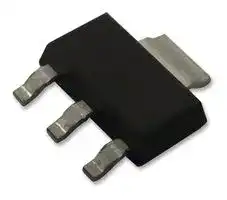


BSP373L6327HTSA1
Power MOSFET, N Channel, 100 V, 1.7 A, 0.16 ohm, SOT-223, Surface Mount
- Manufacturer: INFINEON
- Product type: Single MOSFETs
- Channel Type: N Channel
- Power Dissipation: 1.8W
- Drain Source On State Resistance: 0.16ohm
| Delivery and price | |
|---|---|
| Units per pack | 1000 |
| Price | Ask for quotation |
| Current stock | 10+ |
| Lead time | 30 days |
**==> picture [57 x 11] intentionally omitted <==**

**----- Start of picture text -----**<br>
BSP 373<br>**----- End of picture text -----**<br>


## **SIPMOS[ ®] Small-Signal Transistor**

- N channel

- Enhancement mode

- Avalanche rated

- V = 2.1 ... 4.0 V GS(th)

- Pb-free lead plating; RoHS compliant available

Pin 1 Pin 2 Pin 3 Pin 4 G D S D —--++ ++

> **Type VDS ID RDS(on) Package Marking** BSP 373 100 V 1.7 A 0.3 Ω PG-SOT-223 BSP 373 $$pp pt **Type RoHS compliant Tape and Reel Information** BSP 373 No E6327 BSP 373 Yes L6327

|**Maximum Ratings**||||
|---|---|---|---|
|**Parameter**|**Symbol**<br>ee|**Values**<br>ee|**Unit**|
|Continuous drain current<br>TA= 28 ˚C|ID<br>Pf|1.7<br>Pf|A|
|DC drain current, pulsed<br>TA= 25 ˚C|IDpuls<br>>|6.8<br>>||
|Avalanche energy, single pulse<br>ID= 1.7 A,VDD= 25 V,RGS= 25Ω<br>L= 23.3 mH,Tj= 25 ˚C|EAS<br>>|45<br>>|mJ|
|Gate source voltage|VGS<br>ee|±20<br>ee|V|
|Power dissipation<br>TA= 25 ˚C|Ptot<br>Pop|1.8<br>Pop|W|


Rev 1.1

1

2005-10-27

**BSP 373**

|**Maximum Ratings**||||
|---|---|---|---|
|**Parameter**|**Symbol**<br>ee|**Values**<br>ee|**Unit**|
|Chip or operating temperature|Tj<br>ee<br>ee|-55 ... + 150<br>ee<br>ee|˚C|
|Storage temperature|Tstg<br>ee<br>es|-55 ... + 150<br>ee<br>es||
|Thermal resistance, chip to ambient air|RthJA<br>a|≤70<br>|K/W|
|Thermal resistance, junction-soldering point 1)|RthJS<br>ee|≤10<br>ee||
|DIN humidity category, DIN 40 040|a|E<br>||
|IEC climatic category, DIN IEC 68-1|aes|55 / 150 / 56<br>es||


1) Transistor on epoxy pcb 40 mm x 40 mm x 1,5 mm with 6 cm[2] copper area for drain connection

|Drain- source breakdown voltage<br>VGS= 0 V,ID= 0.25 mA,Tj= 0 ˚C|V(BR)DSS<br>~~|~~|100<br>~~|~~<br>||-<br>~~|~~<br>||-<br>~~|~~|V|
|---|---|---|---|---|---|
|Gate threshold voltage<br>VGS=VDS,ID= 1 mA|VGS(th)<br>CC|2.1<br>|<br>CC|3<br>|<br>CC|4<br>CC||
|Zero gate voltage drain current<br>VDS= 100 V,VGS= 0 V,Tj= 25 ˚C<br>VDS= 100 V,VGS= 0 V,Tj= 125 ˚C|IDSS<br>CC|-<br>-<br>CC<br>ft|10<br>0.1<br>CC<br>ft||100<br>1<br>CC<br>||µA|
|Gate-source leakage current<br>VGS= 20 V,VDS= 0 V|IGSS<br>||-<br>|<br>ft<br>ft|10<br>|<br>ft|<br>ft<br>ft|100<br>|<br>|<br>ft|nA|
|Drain-Source on-state resistance<br>VGS= 10 V,ID= 1.7 A|RDS(on)<br>Pf|-<br>ft<br>Pf<br>ft|0.16<br>ft |<br>Pf<br>ft<br>ft|0.3<br>|<br>Pf<br>ft|Ω|


Rev 1.1

2

2005-10-27

**BSP 373**

> **Electrical Characteristics,** at Tj = 25˚C, unless otherwise specified

|Transconductance<br>VDS≥2*ID *RDS(on)max,ID= 1.7 A|gfs<br>~~|~~|1.5<br>~~|~~<br>fT<br>fT|2.8<br>~~|~~<br>fT|<br>fT||-<br>~~|~~<br>|<br>||S|
|---|---|---|---|---|---|
|Input capacitance<br>VGS= 0 V,VDS= 25 V,f= 1 MHz|Ciss<br>~~|~~|-<br>fT<br>~~|~~<br>fT<br>||400<br>fT |<br>~~|~~<br>fT|<br>|||550<br>|<br>~~|~~<br>|<br>||pF|
|Output capacitance<br>VGS= 0 V,VDS= 25 V,f= 1 MHz|Coss<br>||-<br>fT<br>|<br>|<br>||125<br>fT |<br>|<br>||<br>|||190<br>|<br>|<br>|<br>|||
|Reverse transfer capacitance<br>VGS= 0 V,VDS= 25 V,f= 1 MHz|Crss<br>||-<br>|<br>|<br>||70<br>| |<br>|<br>|||105<br>|<br>|<br>|||
|Turn-on delay time<br>VDD= 30 V,VGS= 10 V,ID= 0.3 A<br>RGS= 50Ω|td(on)<br>|<br>ae|-<br>|<br>|<br>ae|10<br>|<br>||<br>ae|15<br>|<br>|<br>ae|ns|
|Rise time|tr<br>ft|ft|ft|ft||
||ft|ft|ft|ft||
||ft|-<br>ft|30<br>ft|45<br>ft||
||td(off)<br>aan|aan|aan|aan||
||aan|aan|aan|aan||
||aan|-<br>aan|85<br>aan|115<br>aan||
||tf<br>fae|fae|fae|fae||
||fae|fae|fae|fae||
||fae|-<br>fae|60<br>fae|80<br>fae||


Rev 1.1

3

2005-10-27

**BSP 373**

> **Electrical Characteristics,** at Tj = 25˚C, unless otherwise specified

|**Parameter**<br>**Symbol**<br>**Values**<br>**Unit**<br>**min.**<br>**typ.**<br>**max.**<br>OE|**Parameter**<br>**Symbol**<br>**Values**<br>**Unit**<br>**min.**<br>**typ.**<br>**max.**<br>OE|**Parameter**<br>**Symbol**<br>**Values**<br>**Unit**<br>**min.**<br>**typ.**<br>**max.**<br>OE|**Parameter**<br>**Symbol**<br>**Values**<br>**Unit**<br>**min.**<br>**typ.**<br>**max.**<br>OE|
|---|---|---|---|
|**Reverse Diode**||||
|Inverse diode continuous forward current<br>TA= 25 ˚C<br>Inverse diode direct current,pulsed<br>TA= 25 ˚C<br>Inverse diode forward voltage<br>VGS= 0 V,IF= 1.7 A,Tj= 25 ˚C<br>Reverse recovery time<br>VR= 30 V,IF=lS,diF/dt= 100 A/µs<br>Reverse recovery charge<br>VR= 30 V,IF=lS,diF/dt= 100 A/µs|IS<br>-<br>-<br>1.7<br>ISM<br>-<br>-<br>6.8<br>VSD<br>-<br>0.8<br>1.1<br>trr<br>-<br>-<br>-<br>Qrr<br>-<br>-<br>-<br>~~tf~~<br>| |<br>~~|~~<br>ft<br>|<br>| |<br>ft<br>| |<br>et<br>ft<br>ft||A<br>V<br>ns<br>µC|


Rev 1.1

4

2005-10-27

**BSP 373**

## **Power dissipation**

Ptot = ƒ (TA)

## **Drain current**

ID = ƒ (TA) parameter: VGS ≥ 10 V

**==> picture [478 x 255] intentionally omitted <==**

**----- Start of picture text -----**<br>
2.0  PT TTT TTP eee ey yy 1.8  TTTT<br>W  SERRE TTI<br>AREERmv EEE EHH] A  TOR$NCECECOCKE. Ee<br>P 1.6  SECA I COCCCASEEEE EEE<br>tot D 1.4<br>1.4  SEEEINCEEEEEEEEEEPT TEIN; TP TT | yy YT CECEECRSEE\ \ Eee<br>1.2<br>SERRENS | Pi ET tT TT NE E TTN<br>1.2  Pitt TTA Ey ee yt PET TTT [TE]<br>1.0<br>1.0  ELSE, EE E TT<br>flit 0.8  \<br>A i tt APE tt PET TTT TTT TT TET TT<br>0.8  AA EH SESS<br>it ttt tN 0.6  POCAeeee eee<br>0.6<br>HEE ANN EHH PEEEE EEE<br>SEEEEEEEEE ENCE SECC<br>0.4<br>0.4  Pt tty Tee TIN | TY \<br>PEC EELELeeele NLL PT eT TET yy Ty yyy Ar<br>0.2  PEEPPET Tt tT tt ey TATNE 0.2  PTTPi ET TTTTTTEyTTETTEyTy TY<br>0.0  0.0<br>PTT TTT PP rr rr rin PET TTT ETT Te yy<br>0 20 40 60 80 100 120 ˚C 160 0 20 40 60 80 100 120 ˚C 160<br>—_> TA —_» TA<br>**----- End of picture text -----**<br>


**Safe operating area** ID=f(VDS) parameter : D = 0, TC=25˚C

**Transient thermal impedance** Zth JA = ƒ (tp) parameter: D = t / T p

**==> picture [235 x 260] intentionally omitted <==**

**----- Start of picture text -----**<br>
10 2<br>K/W<br>Frnt Cn TT mT mL uy<br>10 1<br>Z<br>thJA<br>10 0  SSae<br>sit Tt So <i<br>10 -1<br>FHT FAH SENSS D = 0.50<br>10 -2  UU TU eTNUNN Uf<br>0.20<br>ST SNES Et 0.10 Itt<br>10 -3<br>0.05<br>STESSA oONSSSH FA<br>POH single pulse NH 0.02<br>10 -4  AN A 0.01<br>a<br>10 -5  PUNEET CO<br>10  [-8 ] 10  [-7 ] 10  [-6 ] 10  [-5 ] 10  [-4 ] 10  [-3 ] 10  [-2 ] 10  [-1 ] s  10  [0 ]<br>— t<br>p<br>**----- End of picture text -----**<br>


Rev 1.1

2005-10-27

5

**BSP 373**

## **Typ. output characteristics**

ID = ƒ( VDS) parameter: tp = 80 µs

**Typ. drain-source on-resistance** RDS (on) = ƒ( ID) parameter: tp = 80 µs, Tj = 25 ˚C

**==> picture [474 x 256] intentionally omitted <==**

**----- Start of picture text -----**<br>
3.8 A ww Ptot lkijhgf  = 2W ed c | | | | tt 0.9  a b<br>Ω<br>SE ELLEELLE<br>3.2  VGS [V]<br>ID a 4.0 RDS (on) 0.7<br>2.8  : oo b 4.5 ELLE<br>c 5.0<br>b 0.6<br>a. 2.4  | d 5.5 VEE<br>e 6.0<br>[A f 6.5 0.5  EAL EE<br>2.0<br>g 7.0<br>2 | h 7.5 0.4  LLL<br>1.6  0 | ee i 8.0 wa ‘<br>a j 9.0 LLLP<br>0.3<br>1.2  k 10.0<br>fF a l 20.0 ry]  | c<br>0.8  || A aonee 0.2  eeSear TT LEED l ikegjhdf<br>0.4  0.1  V GS a  [V] b= c d e f g h i j k l<br>WE | | tT 4.0 4.5 5.0 5.5 6.0 6.5 7.0 7.5 8.0 9.0 10.0 20.0<br>0.0  P| | |fttt 0.0<br>0.0 0.5 1.0 1.5 2.0 2.5 3.0 3.5 4.0 V 5.0 0.0 0.4 0.8 1.2 1.6 2.0 A 2.8<br>V I<br>DS D<br>**----- End of picture text -----**<br>


Typ. transfer characteristics ID = f(VGS) parameter: tp = 80 µs

Typ. forward transconductance gfs = f (ID) parameter: tp = 80 µs,

**==> picture [224 x 253] intentionally omitted <==**

**----- Start of picture text -----**<br>
6.5  CELE ELLE<br>A<br>5.5<br>TCCEE ECE<br>ID 5.0  EEE<br>4.5<br>TTT Tyr<br>4.0<br>titTCE ttt<br>3.5<br> COPEL EE<br>3.0  Ss<br>2.5<br>ttt<br>TCC OPEE Lo<br>2.0<br>1.5  TOO OIPCEL EE<br>1.0<br>tiiCOCOPi tt tt<br>0.5<br>EEL Ee<br>0.0<br>TEEPE<br>0 1 2 3 4 5 6 7 8 V 10<br>V<br>GS<br>**----- End of picture text -----**<br>


**==> picture [226 x 253] intentionally omitted <==**

**----- Start of picture text -----**<br>
4.5  p=<br>S<br>HE ett<br>gfs 3.5 3.0  TELETELL LET LLELL<br>2.5  LYALL4) EEL<br>/<br>ALLL EEL<br>2.0  VALLE  LLL<br>1.5  ALLELE<br>1.0 0.5  FEEL<br>LLL EEL<br>|<br>0.0  PELLEE<br>0.0 1.0 2.0 3.0 4.0 A 6.0<br>I<br>D<br>**----- End of picture text -----**<br>


Rev 1.1

6

2005-10-27

**BSP 373**

## **Drain-source on-resistance**

RDS (on) = ƒ (Tj) parameter: ID = 1.7 A, VGS = 10 V

## **Gate threshold voltage**

VGS (th) = ƒ (Tj) parameter: VGS = VDS, ID = 1 mA

**==> picture [481 x 254] intentionally omitted <==**

**----- Start of picture text -----**<br>
0.75 4.6<br>Ω TT DELCELELELLS, V TRLPLELELLELLL<br>98%<br>PEPE Ty Se EEE<br>0.65 4.0<br>R 0.60 PT tt ett ye V I<br>DS (on) GS(th) 3.6<br>0.55<br>FEEEEEEL EE ERE<br>3.2  typ<br>0.50<br>itt tty tt i<br>0.450.40 PtPt tt| ey| yy| 98% ft tbe_| ee 2.8 2.4  aptta ffffet 2%<br>0.35<br>CAE PRR EEE<br>2.0<br>0.30 ett | treet Tt YT i a s<br>0.25 COE 1.6  EEE se<br>0.20 pF] | | fT typ eet | 1.2  PPPrPrrerrertrt<br>0.15 peer EEE<br>0.8<br>0.10 i—+TT | | | Et td PPPPrrerrertrtyEE<br>0.4<br>0.05 Pi 1<br>0.00 0.0<br>Pt tt| | ftttte TtEE ytEE Soa<br>-60 -20 20 60 100 ˚C 160 -60 -20 20 60 100 ˚C 160<br>T T<br>j j<br>**----- End of picture text -----**<br>


## **Typ. capacitances**

C = f (VDS) parameter:VGS=0V, f = 1 MHz

**Forward characteristics of reverse diode** IF = ƒ (VSD) parameter: Tj, tp = 80 µs

**==> picture [224 x 257] intentionally omitted <==**

**----- Start of picture text -----**<br>
10 1<br>eG |<br>nF<br>es<br>C<br>10 0<br>pop ee[ —tteettt ee<br>| C<br>iss<br>AX<br>Se<br>10 -1  SI Coss<br>C<br>a rss<br>a |<br>ss OO<br>P| |<br>10 -2  ELLE ELE<br>0 5 10 15 20 25 30 V 40<br>V<br>DS<br>**----- End of picture text -----**<br>


**==> picture [223 x 259] intentionally omitted <==**

**----- Start of picture text -----**<br>
10 1<br>i<br>A<br>Sen Sey 4eee<br>I<br>F<br>10 0<br>Lf<br>+ ASe<br>en i eeeee<br>—A<br>28 Pee<br>10 -1  ane aaa<br>Tj = 25 ˚C typ<br>= So ===<br>ee | Tj = 150 ˚C typ L [ [ |<br>EIS Tj = 25 ˚C (98%) TT<br>Tj = 150 ˚C (98%)<br>Ps ane<br>10 -2  Lhe AL<br>0.0 0.4 0.8 1.2 1.6 2.0 2.4 V 3.0<br>V<br>SD<br>**----- End of picture text -----**<br>


Rev 1.1

2005-10-27

7

**BSP 373**

**Avalanche energy** EAS = ƒ (Tj) parameter: ID = 1.7 A, VDD = 25 V RGS = 25 Ω , L = 23.3 mH

**Drain-source breakdown voltage** V(BR)DSS = ƒ (Tj)

**==> picture [476 x 256] intentionally omitted <==**

**----- Start of picture text -----**<br>
50 120<br>V<br>mJ TLL EEE PE TT TT TT ty<br>116<br>E 40 ATLEEELLLLLELT\ V 114 peFCCP EEEeeeerbE |<br>AS (BR)DSS<br>112<br>35<br>110<br>f NEELLCONCEP ELLE LLL PPPEER Pry ry<br>30 108<br>TENEELL ELLE 106 OEE[ettAr<br>25<br>104<br>CCOCN\ EE SCEtt yay<br>20 102 PPP<br>TLLEN 100 AT<br>15  TELL pit ttaA ttt tt |<br>98<br>CCECEEINELEE SRE EE<br>10 96<br>ELLE \ 94 OATES<br>5 LLNELLE Jz t ttt tt tt<br>92<br>0 ON 90 ee<br>20 40 60 80 100 120 ˚C 160 -60 -20 20 60 100 ˚C 160<br>—r Tj —_— r Tj<br>**----- End of picture text -----**<br>


**Safe operating area** ID=f(VDS) parameter : D = 0.01, TC=25˚C

Rev 1.1

8

2005-10-27
Updated at February 9, 2023
Infineon Technologies is a globally recognized leader in semiconductor solutions, renowned for driving innovation in power management, energy efficiency, and modern mobility. With a strong legacy of engineering excellence, the company provides highly reliable components designed to meet the rigorous demands of industrial, automotive, and advanced commercial applications. The core of our Infineon portfolio is centered on their industry-leading discrete semiconductors. We offer an extensive selection of single and dual MOSFETs, alongside a robust range of single IGBTs and advanced IGBT modules. These flagship power transistors are essential for high-efficiency power conversion and motor control, providing engineers with superior thermal performance and minimized switching losses. Beyond advanced field-effect transistors, the selection includes a comprehensive array of diodes and rectifiers, heavily featuring Schottky diodes, as well as fast-recovery and RF/PIN diodes. This power foundation is further supported by bipolar transistors, intelligent power modules, and thyristor SCR modules, delivering the critical building blocks required for complex power system designs. To support broader system integration, the portfolio also encompasses specialized solutions such as solid-state relays, AC/DC LED driver ICs, and Bluetooth communications modules. From high-power industrial rectifiers to wireless connectivity adapters, Infineon equips designers with the precision components needed to build efficient, scalable, and fully connected electronic systems.
About Novapart
Novapart is a B2B electronic component broker specialising in stock shortages and cost reduction. We source hard-to-find parts and identify compliant alternatives across a catalogue of 410,000+ components from 500+ manufacturers.
Learn more →Stock Shortage Specialist
When a component is unavailable, discontinued or has an unacceptable lead time, we tap into our network of vetted European and Asian distributors to source what you need — without compromising on quality or traceability.
Request a quote →Compliant Alternatives
We identify pin-to-pin, electrically equivalent substitutes that meet the same certifications (RoHS, AEC-Q100, REACH) as your original specification — validated against datasheets, not just part numbers. Often at a lower cost.
BOM Analysis service →