


BSP324H6327XTSA1
Power MOSFET, N Channel, 400 V, 170 mA, 25 ohm, SOT-223, Surface Mount
- Manufacturer: INFINEON
- Product type: Single MOSFETs
- Transistor Polarity:N Channel; Continuous Drain Current Id:170mA; Drain Source Voltage Vds:400V; On Resistance Rds(on):13.6ohm; Rds(on) Test Voltage Vgs:10V; Threshold Voltage Vgs:1.
- MSL: MSL 1 - Unlimited
- SVHC: No SVHC (25-Jun-2025)
- No. of Pins: 4Pins
- Channel Type: N Channel
- Product Range: SIPMOS
- Qualification: AEC-Q101
- Power Dissipation: 1.8W
- Transistor Mounting: Surface Mount
- Rds(on) Test Voltage: 10V
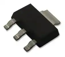
- Transistor Case Style: SOT-223
- Drain Source Voltage Vds: 400V
- Operating Temperature Max: 150°C
- Continuous Drain Current Id: 170mA
- Drain Source On State Resistance: 25ohm
- Gate Source Threshold Voltage Max: 1.9V
| Delivery and price | |
|---|---|
| Units per pack | 500 |
| Price | 0.298 € |
| Current stock | 1000+ |
| Lead time | 30 days |
**BSP324**
Rev. 2.2
## **SIPMOS**[] **Power-Transistor Feature**
- N-Channel
- Enhancement mode
- Logic Level
- d _v_ /d _t_ rated
|_V_DS|400|V|
|---|---|---|
|_R_DS(on)|25|Ω|
|DS(on)<br>_I_D|0.17|A|
- Pb-free lead plating; RoHS compliant Qualified according to AEC Q101
- • Halogenfree according to IEC61249221 °
|**Type**|**Package**|**Pb-free**|**Packaging**|**Tape and Reel Information**|**Marking**|
|---|---|---|---|---|---|
|BSP324|PG-SOT223|Yes|Non dry|H6327: 1000 pcs/reel|BSP324|
|j<br>**Parameter**|**Symbol**|**Value**|**Unit**|
|---|---|---|---|
|Continuous drain current<br>_T_A=25°C<br>_T_A=70°C|_I_D<br>Pf|0.17<br>0.14<br>Pf|A|
|Pulsed drain current<br>_T_A=25°C|_I_D puls|0.68||
|Reverse diode d_v_/d_t_<br>_I_S=0.17A,_V_DS=320V, d_i_/d_t_=200A/µs,_T_jmax=175°C|d_v_/d_t_|6|kV/µs|
|Gate source voltage|_V_GS<br>a|±20<br>a|V|
|ESD Class (JESD22-A114-HBM)||1A (>250V, <500V)||
|Power dissipation<br>_T_A=25°C|_P_tot<br>||1.8<br>||W|
|Operating and storage temperature|_T_j ,_T_stg<br>ee|-55... +150<br>ee|°C|
|IEC climatic category; DIN IEC 68-1|j ,stg<br>a|55/150/56||
20 12 - 11 - 29
Page 1
|Rev.2.2<br>**BSP324**<br>**Thermal Characteristics**<br>**Parameter**<br>**Symbol**<br>**Values**<br>**Unit**<br>**min.**<br>**typ.**<br>**max.**<br>Cofineon~~ee~~|Rev.2.2<br>**BSP324**<br>**Thermal Characteristics**<br>**Parameter**<br>**Symbol**<br>**Values**<br>**Unit**<br>**min.**<br>**typ.**<br>**max.**<br>Cofineon~~ee~~|Rev.2.2<br>**BSP324**<br>**Thermal Characteristics**<br>**Parameter**<br>**Symbol**<br>**Values**<br>**Unit**<br>**min.**<br>**typ.**<br>**max.**<br>Cofineon~~ee~~|Rev.2.2<br>**BSP324**<br>**Thermal Characteristics**<br>**Parameter**<br>**Symbol**<br>**Values**<br>**Unit**<br>**min.**<br>**typ.**<br>**max.**<br>Cofineon~~ee~~|Rev.2.2<br>**BSP324**<br>**Thermal Characteristics**<br>**Parameter**<br>**Symbol**<br>**Values**<br>**Unit**<br>**min.**<br>**typ.**<br>**max.**<br>Cofineon~~ee~~|Rev.2.2<br>**BSP324**<br>**Thermal Characteristics**<br>**Parameter**<br>**Symbol**<br>**Values**<br>**Unit**<br>**min.**<br>**typ.**<br>**max.**<br>Cofineon~~ee~~|Rev.2.2<br>**BSP324**<br>**Thermal Characteristics**<br>**Parameter**<br>**Symbol**<br>**Values**<br>**Unit**<br>**min.**<br>**typ.**<br>**max.**<br>Cofineon~~ee~~|
|---|---|---|---|---|---|---|
||**Characteristics**||||||
||Thermal resistance, junction - soldering point<br>(Pin 4)||_R_thJS|-|16|25<br>K/W|
||SMD version, device on PCB:<br>@ min. footprint<br>@ 6 cm2cooling area1)||_R_thJA|-<br>-|85<br>45|115<br>70|
|Drain-source breakdown voltage<br>_V_GS=0, _I_D=250µA<br>|<br>||_V_(BR)DSS<br>||<br>|||400<br>**|**<br>**|**|-|-|V|
|---|---|---|---|---|---|
|Gate threshold voltage,_V_GS=_V_DS<br>_I_D=94µA<br>|<br>||_V_GS(th)<br>| |<br>|||1.3<br>**|**<br>**|**|1.9|2.3||
|Zero gate voltage drain current<br>_V_DS=400V,_V_GS=0, _T_j=25°C<br>_V_DS=400V,_V_GS=0, _T_j=125°C<br>|<br>||_I_DSS<br>| |<br>Bane<br>|||-<br>-<br>**|**<br>Bane<br>**|**|0.01<br>-<br>Bane|0.1<br>10<br>Bane|µA|
|Gate-source leakage current<br>_V_GS=20V,_V_DS=0<br>|<br>||_I_GSS<br>||<br>|||-<br>**|**<br>**|**|10|100|nA|
|Drain-source on-state resistance<br>_V_GS=4.5V, _I_D=0.05A<br>|<br>|<br>||_R_DS(on)<br>| |<br>||<br>|||-<br>**|**<br>**|**<br>ft|14.3<br>ft|22<br>|Ω|
|Drain-source on-state resistance<br>_V_GS=10V,_I_D=0.17A<br>|<br>||_R_DS(on)<br>| |<br>|||-<br>**|**<br>ft|13.6<br>ft||25<br>|||
1Device on 40mm*40mm*1.5mm epoxy PCB FR4 with 6cm² (single layer, 70 µm thick) copper area for drain connection. PCB is vertical without blown air.
20 12 - 11 - 29
Page 2
**BSP324**
Rev. 2.2
**==> picture [497 x 520] intentionally omitted <==**
**----- Start of picture text -----**<br>
||||||||||||||
|---|---|---|---|---|---|---|---|---|---|---|---|---|
|Electrical Characteristics|, at|T|j = 25 °C, unless otherwise specified|
|Parameter|Symbol|Conditions|Values|Unit|
|min.|typ.|max.|
|ee|er|en|
|Dynamic Characteristics|
|Transconductance|g|fs|V|DS≥2*|I|D*|R|DS(on)max,|0.09|0.19|-|S|
|I|D=0.14A|
|Input capacitance|eee|C|iss|V|GS=0,|V|DS=25V,|-|103|154|pF|
|Output capacitance|C|oss|f|=1MHz|-|9.2|13.6|
|Reverse transfer capacitance|C|rss|-|3.8|5.7|
|Turn-on delay time|===>|t|d(on)|V|DD=225V,|V|GS=10V,|-|4.6|6.9|ns|
|Rise time|t|r|I|D=0.17A,|R|G=6Ω|-|4.4|6.6|
|Turn-off delay time|t|d(off)|-|17|25|
|Fall time|t|f|-|68|102|
|Gate Charge Characteristics|
|Gate to source charge|Q|gs|V|DD|=320V,|I|D|=0.17A|-|0.35|0.45|nC|
|Gate to drain charge|Q|-|2.17|2.82|
|gd|
|Gate charge total|Q|g|V|DD|=320V,|I|D|=0.17A,|-|4.54|5.9|
|V|GS=0 to 10V|
|Gate plateau voltage|V|(plateau)|V|DD|=320V,|I|D|=0.17A|-|3.6|-|V|
|Reverse Diode|
|Inverse diode continuous|I|S|T|A=25°C|-|-|0.17|A|
|forward current|
|Inv. diode direct current, pulsed|I|SM|-|-|0.68|
|Inverse diode forward voltage|V|SD|V|GS=0,|I|F=0.17A|-|0.8|1.2|V|
|Reverse recovery time|t|rr|V|R=200V,|I|F=|l|S,|-|85|127|ns|
|Reverse recovery charge|Q|rr|d|i|F/d|t|=100A/µs|-|104|156|nC|
**----- End of picture text -----**<br>
20 12 - 11 - 29
Page 3
**BSP324**
Rev. 2.2
## **1 Power dissipation** _P_ tot = _f_ ( _T_ A)
## **2 Drain current**
## _I_ D = _f_ ( _T_ A)
## parameter: _V_ GS≥ 10 V
**==> picture [223 x 265] intentionally omitted <==**
**----- Start of picture text -----**<br>
BSP324<br>1.9<br>W PTT tT tT TTT TT Tt<br>PT IN TTT TT TT TT<br>1.6 BERANE PEPREEEEE EP<br>PCAN<br>1.4<br>COCCI<br>1.2<br>CECE AEE<br>CECE EEE<br>1<br>OEE ALLELE<br>TOEETTCe ACE<br>0.8<br>Peeper<br>0.6 FFENee PeeeePeE EXELL<br>0.4 PTTPTE TTT TT TT TTT TTTtT ttTINtNTETTT<br>0.2 PTETPTT TTTTT TTTTTTT TTTTTTTTRETN TI|<br>0 PTET TTT tt ttt tein |<br>0 20 40 60 80 100 120 °C 160<br>T A<br>tot<br>P<br>**----- End of picture text -----**<br>
## **3 Safe operating area**
## _I_ D = _f_ ( _V_ DS )
## parameter : _D_ = 0 , _T_ A = 25 °C
**==> picture [230 x 266] intentionally omitted <==**
**----- Start of picture text -----**<br>
10 1 BSP324<br>A ee ee ee<br>PT ETT TT<br>10 0 CF t p = 170.0µs<br>a ee ee<br>esPTeeTCT TT [AATTTey iIN TT AON TT<br> 1 ms<br>10 -1 PTT Saniiiinsenttt<br>Pet SE 10 ms<br>10 -2 CIM CMEaN<br>Ceo Ce tT DC PUT<br>ell<br>10 -3 ED a<br>10 0 10 1 10 2 V 10 3<br>— V DS<br>I D<br> /<br>V DS<br> =<br>R DS(on)<br>D<br>I<br>**----- End of picture text -----**<br>
**==> picture [224 x 265] intentionally omitted <==**
**----- Start of picture text -----**<br>
BSP324<br>0.18 LETT tT ttt tT yy<br>A<br>TT<br>CCCPNCCCEIEEE Eee<br>NS<br>0.14<br>fa RPfp<br>NH<br>0.12 tN<br>0.1 tN<br>PT TTT TTT TT TAT YT<br>0.08 PT TTT TEE TT TING | To<br>FEE<br>0.06 PT TTT TTT TT TT TNT TI<br>PTT tT TTT TTT TT IN TT<br>0.04 PTT TT TTT Ty TT Ty A<br>PTT TT ett Ty ty At<br>0.02 PT TTT TTT ET Ty TTY<br>PTT TT TTT TT tT tty ty<br>0 LEE TTT TTT TT ttt yt yf<br>0 20 40 60 80 100 120 °C 160<br>T A<br>D<br>I<br>**----- End of picture text -----**<br>
## **4 Transient thermal impedance**
_Z_ thJA = _f_ ( _t_ p)
## parameter : _D_ = _t_ p/ _T_
**==> picture [230 x 267] intentionally omitted <==**
**----- Start of picture text -----**<br>
10 2 BSP324<br>K/W a | | | ee|<br>CUNT TTrT TT TTT<br>10 1 Sa 7TC<br>| aM MT | |)<br>rinSTANTTh NUTT| 1TT TT<br>10 0 BA Ba SU SU<br>D = 0.50<br>0.20<br>| 0 AN A SR 0.10<br>10 -1 R | single pulse OMist time 0.05 |<br>0.02<br>AA A || 0.01 tu<br>UE TUT TT TE ooo<br>10 -2 CTIA LTT<br>-5 -4 -3 -2 -1 0 1 2 4<br>10 10 10 10 10 10 10 10 s 10<br>—_r t p<br>thJA<br>Z<br>**----- End of picture text -----**<br>
20 12 - 11 - 29
Page 4
**BSP324**
Rev. 2.2
## **6 Typ. drain-source on resistance**
## **5 Typ. output characteristic**
_I_ D = _f_ ( _V_ DS)
_R_ DS(on) = _f_ ( _I_ D)
parameter: _T_ j = 25 °C, _V_ GS
parameter: _T_ j = 25 °C, _V_ GS
**==> picture [481 x 598] intentionally omitted <==**
**----- Start of picture text -----**<br>
0.6 22<br>Ω<br>TiiilB HAH<br>18<br>16<br>0.4<br>14<br>12<br>0.3 10V 3.7V<br>7V 10 3.9V<br>6V 4.1V<br>LD Zan 5V e772 8 4.3V<br>0.2<br>4.5V 4.5V<br>4.3V 6 5V<br>4.1V 6V<br>0.1 3.9V 4 7V<br>3.7V 10V<br>2<br>AL if<br>0 0<br>0 1 2 3 4 5 6 7 8 10 0 0.05 0.1 0.15 0.2 0.25 A 0.35<br>I D<br>7 Typ. transfer characteristics 8 Typ. forward transconductance<br>D== f ( V GS ); ); V DS≥ 2 x ≥ 2 x 2 x I D x x R DS(on)max g fs = f( I D)<br>parameter: T j = 25 °C = 25 °C parameter: T j = 25 °C<br>0.35 0.36<br>S<br>A<br>0.28<br>FEE CCIE<br>0.25<br>0.24<br>0.2<br>PET 0.2 Ee<br>| | TE) ffi 0.16 GereTTYL<br>0.15<br>0.12<br>0.1<br>0.08<br>P ETE YT) tA<br>0.05<br>PT EET | ) 0.04 fee<br>LEE<br>0 | YE | 0 PT<br>0 1 2 3 V 5 0 0.05 0.1 0.15 0.2 0.25 A 0.35<br>V GS I D<br> DS(on)<br>R<br>D fs<br>I g<br>**----- End of picture text -----**<br>
## **7 Typ. transfer characteristics**
_I_ D== _f_ ( _V_ GS ); ); _V_ DS≥ 2 x ≥ 2 x 2 x _I_ D x x _R_ DS(on)max parameter: _T_ j = 25 °C = 25 °C
20 12 - 11 - 29
Page 5
**BSP324**
## Rev. 2.2
## **9 Drain-source on-state resistance**
_R_ DS(on) = _f_ ( _T_ j)
## parameter : _I_ D = 0.17 A, _V_ GS = 10 V
**==> picture [226 x 267] intentionally omitted <==**
**----- Start of picture text -----**<br>
BSP324<br>130<br>Ω SERRE<br>110<br>SERRE<br>100<br>SERRE<br>90<br>80 ttt T ETT Ey Ty<br>SERRE<br>70<br>60<br>50 Pt Tt te tT ET eT T<br>SERRE<br>40<br>ttt 98% -<br>30 |_|. bey Te<br>20<br>10 Ease: typ iT | |<br>0 PTET TETaTETeEy<br>-60 -20 20 60 100 °C 180<br>—_> T j<br> DS(on)<br>R<br>**----- End of picture text -----**<br>
## **10 Typ. gate threshold voltage** _V_ GS(th) = _f_ ( _T_ j) parameter: _V_ GS = _V_ DS; _I_ D =94µA
**==> picture [226 x 264] intentionally omitted <==**
**----- Start of picture text -----**<br>
2.6<br>V tsiIm, | ftbb ttbd tadbb bddot<br>it a ee<br>TST 98%<br>2.2<br>pip Psa<br>LootI | I I tt| | Pstx! I | |<br>2 boop fa—t =p tna b tt<br>| | | | | typ. | | | bee<br>1.8 aWEE DNL ERAS<br>PP Neer<br>a|| ae | a fof phe<br>|||<br>1.6<br>i<br>1.4 Popo pp<br>A SR e e 2%<br>1 | | | | ~ | | | | | |<br>Poy| I | tA | I IN| I | I I |<br>1.2 eePy eesPPies Wee rpee aie str Sei ee ee eee |<br>1<br>|<br>0.8<br>ae Sng Op ON OD) |<br>0.6 Setpinatebpdel desettnet enti|<br>-60 -20 20 60 100 °C 160<br>er Tj<br>- VGS(th)<br>**----- End of picture text -----**<br>
## **11 Typ. capacitances** _C_ = _f_ ( _V_ DS)
## parameter: _V_ GS=0, _f_ =1 MHz, _T_ j = 25 °C
**==> picture [223 x 265] intentionally omitted <==**
**----- Start of picture text -----**<br>
10 3 pros yr===4zS===yzS===yT====yA====4<br>pF bocortrcrstorrictrrtaatssaaAstaaa4CTTa7 TT TTT TaTata TT ATTaTT ATTaTT ATTTTIA<br>esT T T T 7 7<br>a es ee<br>Ciss<br>10 2<br>Se | | | | |<br>pop==f==-=4f--==f=<==4-===4====4ee ee ee ee<br>Lp——t____ a tedtd<br>aL-§AL\ es ee Coss ee-—t_--____J____-]<br>A<br>| | | ' | | |<br>|| 10 1 || | | | || || ||<br>Cla TTIAsQ. ata Crss SS SOGSRSSIGIE [SSSR<br>pIDIIyII=Ssyocom (DIQIIIIGII=I=Ig<br>}——--4—--L--__1__4} ee} ----4<br>!--—--4+—-—--4----4----4----4---| | | ee | —|__.___]4<br>| | | | | | |<br>b--__4—~—~_4-—-—~—_4-—~~-—_—4-—~—~~—-—~-—~~—4<br>| | | | | | |<br>10 0 |[a | en | en I in Sn| [ese| ||<br>0 5 10 15 20 V 30<br>V<br>DS<br>C<br>**----- End of picture text -----**<br>
## **12 Forward character. of reverse diode** _I_ F = _f_ (V SD)
## parameter: _T_ j
**==> picture [221 x 266] intentionally omitted <==**
**----- Start of picture text -----**<br>
10 0 propr=Fr=Frzr=Az=sz=4z=A={A=j{A=s{A=AjA=AjA=AjA=A BSP324<br>A fotototototctctotsatcatatC=I=I=I= TIT ATATATATA as asde)a a s<br>a an (ES ss ca<br>BENPTT TPT s ue aaeneenTT Ua TTT1<br>HE A<br>10 -1<br>11 | 7<br>PattF=t=t ohop4th ep t -4-4-4-4-4-4-4-4-atasasa4=d=ses=s =4<br>LLLCAE+f tetetedett dd<br>nt)L_-L_Lip2)re—t—t—t—it-_t-_i-_-j_-_ te<br>| [ee ee 2s ee | ee ee |<br>A| 10 -2 totIt totUWtmriT otfottb rot t t btt tbto ttottott tottot<br>C-iI-y¥er stTHie Iseai T j = 25 °C typ JZ3=3=4a or |<br>eSL_L_#_tot a# We4tsdie eeett ~ T j = 150 °C typ re|I a | eeee P| aetol<br>aoot & W~l | T j = 25 °C (98%) \-4-4-4I t t |<br>—i tmas Bett T j = 150 °C (98%) {-4—4-4It 1 |<br>10 -3 LoL! | i —-H-1-te fototrotrotrotoet tt tttore TTt t T tot<br>0 0.4 0.8 1.2 1.6 2 2.4 V 3<br>V<br>—_—_—- _} SD<br>F<br>I<br>**----- End of picture text -----**<br>
20 12 - 11 - 29
Page 6
**BSP324**
Rev. 2.2
## **13 Typ. gate charge**
_V_ GS = _f_ ( _Q_ G); parameter: _V_ DS ,
## **14 Drain-source breakdown voltage**
_V_ (BR)DSS = _f_ ( _T_ j)
## _I_ D = 0.17 A pulsed, _T_ j = 25 °C
**==> picture [481 x 267] intentionally omitted <==**
**----- Start of picture text -----**<br>
BSP324 BSP324<br>16 490<br>V<br>PET TTT ET ET ty Tt<br>V<br>470<br>460<br>12 PETSSGGG000TTT TT [ITAAAL] 4/4000I 450 TET<br>10 Pit TT Ty AAT Tt 440 SERRET TTT TT ye<br>0.2 V DS max tL AAA LI I 430 PE LTE TTT A tt<br>8 0.5 V DS max<br>AHHH 420 PT eT ETye<br>0.8 V DS max<br>6 410<br>| WALT)NIAAA LT Tt f SERRE YjAe<br>400<br>4<br>LE TAAAWV TTTit tt dttt 390 P PTT i tTytAtty yt tt<br>fine eee TT TA TT TTT PTT] i<br>380<br>2<br>TET TTT ET ET ty ty > ~neneeeeeee<br>370<br>Pid i tid tty yt ty 4<br>PCC PEELE<br>0 360 EL ELE LE<br>0 1 2 3 4 5 nC 7 -60 -20 20 60 100 °C 180<br>Q G T j<br>GS (BR)DSS<br>V V<br>**----- End of picture text -----**<br>
20 12 - 11 - 29
Page 7
**BSP324**
Rev 2.2
20 12 - 11 - 29
Page 8
Updated at April 29, 2026
Infineon Technologies is a globally recognized leader in semiconductor solutions, renowned for driving innovation in power management, energy efficiency, and modern mobility. With a strong legacy of engineering excellence, the company provides highly reliable components designed to meet the rigorous demands of industrial, automotive, and advanced commercial applications. The core of our Infineon portfolio is centered on their industry-leading discrete semiconductors. We offer an extensive selection of single and dual MOSFETs, alongside a robust range of single IGBTs and advanced IGBT modules. These flagship power transistors are essential for high-efficiency power conversion and motor control, providing engineers with superior thermal performance and minimized switching losses. Beyond advanced field-effect transistors, the selection includes a comprehensive array of diodes and rectifiers, heavily featuring Schottky diodes, as well as fast-recovery and RF/PIN diodes. This power foundation is further supported by bipolar transistors, intelligent power modules, and thyristor SCR modules, delivering the critical building blocks required for complex power system designs. To support broader system integration, the portfolio also encompasses specialized solutions such as solid-state relays, AC/DC LED driver ICs, and Bluetooth communications modules. From high-power industrial rectifiers to wireless connectivity adapters, Infineon equips designers with the precision components needed to build efficient, scalable, and fully connected electronic systems.
About Novapart
Novapart is a B2B electronic component broker specialising in stock shortages and cost reduction. We source hard-to-find parts and identify compliant alternatives across a catalogue of 410,000+ components from 500+ manufacturers.
Learn more →Stock Shortage Specialist
When a component is unavailable, discontinued or has an unacceptable lead time, we tap into our network of vetted European and Asian distributors to source what you need — without compromising on quality or traceability.
Request a quote →Compliant Alternatives
We identify pin-to-pin, electrically equivalent substitutes that meet the same certifications (RoHS, AEC-Q100, REACH) as your original specification — validated against datasheets, not just part numbers. Often at a lower cost.
BOM Analysis service →