


BSP315PH6327XTSA1
Power MOSFET, P Channel, 60 V, 1.17 A, 0.8 ohm, SOT-223, Surface Mount
- Manufacturer: INFINEON
- Product type: Single MOSFETs
- Transistor Polarity:P Channel; Continuous Drain Current Id:-1.17A; Drain Source Voltage Vds:-60V; On Resistance Rds(on):0.5ohm; Rds(on) Test Voltage Vgs:-10V; Threshold Voltage Vgs:
- MSL: MSL 1 - Unlimited
- SVHC: No SVHC (25-Jun-2025)
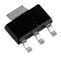
- No. of Pins: 4Pins
- Channel Type: P Channel
- Product Range: -
- Qualification: -
- Power Dissipation: 1.8W
- Transistor Mounting: Surface Mount
- Rds(on) Test Voltage: 10V
- Transistor Case Style: SOT-223
- Drain Source Voltage Vds: 60V
- Operating Temperature Max: 150°C
- Continuous Drain Current Id: 1.17A
- Drain Source On State Resistance: 0.8ohm
- Gate Source Threshold Voltage Max: 1.5V
| Delivery and price | |
|---|---|
| Units per pack | 500 |
| Price | 0.271 € |
| Current stock | 1000+ |
| Lead time | 30 days |
**BSP315P** ## **SIPMOS**[] **Small-Signal-Transistor** ## **Features** ## **Product Summary** - P-Channel P-Channel **==> picture [487 x 178] intentionally omitted <==** **----- Start of picture text -----**<br> |||||||| |---|---|---|---|---|---|---| |P-Channel P-Channel|Drain source voltage|VDS|-60|V| |• Enhancement mode Enhancement mode|Drain-Source on-state resistance|RDS(on)|0.8|Ω| |• Avalanche rated|Continuous drain current|ID|-1.17|A| |• Logic Level| |4| |• dv/dt rated|EO| |Pin 1|Pin2/4|PIN 3| |G|D|S|3| |•|¢ Pb-free|Qualified according to AEC Q101|lead plating; ROHS compliant|—-—-|+ ZBQESES|2| |•|1|VPS05163| |Halogenfree according to IEC61249221|RoHS|~~|S—| |en|(<|) Halogen-Free|S/|fect *| **----- End of picture text -----**<br> - Enhancement mode Enhancement mode **==> picture [486 x 412] intentionally omitted <==** **----- Start of picture text -----**<br> |||||| |---|---|---|---|---| |Type|Package|Tape and Reel Information|Marking|Packaging| |BSP315P|PG-SOT223|H6327: 1000 pcs/reel|BSP315P|Non dry| |Maximum Ratings|,at Tj = 25 °C, unless otherwise specified| |Parameter|a|Symbol|Value|Unit| |Continuous drain current|ID|A| |TA = 25 °C|-1.17| |TA = 70 °C|-0.94| |Pulsed drain current|I|-4.68| |D puls| |TA = 25 °C| |Avalanche energy, single pulse|EAS|24|mJ| |ID = -1.17 A , VDD = -25 V, RGS = 25 Ω| |Avalanche energy, periodic limited by Tjmax|a|EAR|0.18| |Reverse diode dv/dt|dv/dt|6|kV/µs| |IS = -1.17 A, VDS = -48 V, di/dt = 200 A/µs,| |T|= 150 °C| |jmax| |Gate source voltage|a|VGS|±20|V| |Power dissipation|Ptot|1.8|W| |TA = 25 °C| |Operating and storage temperature|a|Tj , Tstg|-55...+150|°C| |IEC climatic category; DIN IEC 68-1|ee|55/150/56| |ESD Class; JESD22-A114-HBM|Class 0| |ee| **----- End of picture text -----**<br> 2012-11-26 Rev.1.7 Page 1 **BSP315P** **Thermal Characteristics** |**Thermal Characteristics**|||||| |---|---|---|---|---|---| |**Parameter**<br>**Characteristics**<br>~~ee ~~|**Symbol**<br>|**Unit**<br>**Values**<br>**min.**<br>**max.**<br>**typ.**<br> ~~ee~~|||| |Thermal resistance, junction - soldering point|RthJS|-|-|25|K/W| |(Pin 4)|||||| |SMD version, device on PCB:|RthJA||||K/W| |@ min. footprint||-|-|115|| |@ 6 cm2cooling area1)||-|-|70|| |Drain- source breakdown voltage<br>VGS= 0 V, ID= -250 µA<br>||V(BR)DSS<br>||<br>S||-60<br>**|**<br>S|tt|-<br>tt|-<br>tt|V| |---|---|---|---|---|---| |Gate threshold voltage, VGS= VDS<br>ID= -160 µA<br>||VGS(th)<br>| |<br>S||-1<br>**|**<br>S|tt|-1.5<br>tt|-2<br>tt|| |Zero gate voltage drain current<br>VDS= -60 V, VGS= 0 V, Tj= 25 °C<br>VDS= -60 V, VGS= 0 V, Tj= 125 °C<br>||IDSS<br>S|<br>tty<br>|||-<br>-<br>S| tt<br>tty<br>**|**|-0.1<br>-10<br>tt<br>tty|-1<br>-100<br>tt<br>tty|µA| |Gate-source leakage current<br>VGS= -20 V, VDS= 0 V<br>|<br>||IGSS<br>||<br>|||-<br>**|**<br>**|**|-10|-100|nA| |Drain-Source on-state resistance<br>VGS= -4.5 V, ID= -0.89 A<br>|<br>|<br>||RDS(on)<br>| |<br>||<br>|<br>|tt|-<br>**|**<br>**|**<br>tt|0.8<br>tt|1.4<br>tt|Ω| |Drain-Source on-state resistance<br>VGS= -10 V, ID= -1.17 A<br>|<br>||RDS(on)<br>| |<br>|<br>|tt|-<br>**|**<br>tt|0.5<br>tt|0.8<br>tt|Ω| > 1Device on 40mm*40mm*1.5mm epoxy PCB FR4 with 6cm2 (one layer, 70 µm thick) copper area for drain connection. PCB is vertical without blown air. 2012-11-26 Rev.1.7 Page 2 |Transconductance<br>VDS≤2*ID*RDS(on)max, ID= -0.89 A|gfs<br>pt<br>pf}|0.7<br>pt<br>|<br>pf}|1.4<br>pt<br>|<br>|-<br>pt<br>|S| |---|---|---|---|---|---| |Input capacitance<br>VGS= 0 V, VDS= -25 V, f = 1 MHz|Ciss<br>pf}|-<br>|<br>pf} tt<br>||130<br>|<br>tt<br>||160<br>tt|pF| |Output capacitance<br>VGS= 0 V, VDS= -25 V, f = 1 MHz|Coss<br>pf}<br>of|-<br>|<br>pf} <br>of<br>||40<br>|<br><br>of<br>||50<br><br>of|| |Reverse transfer capacitance<br>VGS= 0 V, VDS= -25 V, f = 1 MHz|Crss|-<br>||17<br>||21|| |Turn-on delay time<br>VDD= -30 V, VGS= -4.5 V, ID= -0.89 A,<br>RG= 18Ω|td(on)|-|24|36|ns| |Rise time<br>VDD= -30 V, VGS= -4.5 V, ID= -0.89 A,<br>RG= 18Ω|tr|-|9|14|| |Turn-off delay time<br>VDD= -30 V, VGS= -4.5 V, ID= -0.89 A,<br>RG= 18Ω|td(off)|-|32|48|| |Fall time<br>VDD= -30 V, VGS= -4.5 V, ID= -0.89 A,<br>RG= 18Ω|tf|-|19|28|| 2012-11-26 Rev.1.7 Page 3 |**BSP315P**<br>**Electrical Characteristics,**at Tj= 25 °C, unless otherwise specified<br>**Unit**<br>**Values**<br>**Symbol**<br>**Parameter**<br>**min.**<br>**typ.**<br>**max.**<br>Gafineonee|**BSP315P**<br>**Electrical Characteristics,**at Tj= 25 °C, unless otherwise specified<br>**Unit**<br>**Values**<br>**Symbol**<br>**Parameter**<br>**min.**<br>**typ.**<br>**max.**<br>Gafineonee|**BSP315P**<br>**Electrical Characteristics,**at Tj= 25 °C, unless otherwise specified<br>**Unit**<br>**Values**<br>**Symbol**<br>**Parameter**<br>**min.**<br>**typ.**<br>**max.**<br>Gafineonee|**BSP315P**<br>**Electrical Characteristics,**at Tj= 25 °C, unless otherwise specified<br>**Unit**<br>**Values**<br>**Symbol**<br>**Parameter**<br>**min.**<br>**typ.**<br>**max.**<br>Gafineonee|**BSP315P**<br>**Electrical Characteristics,**at Tj= 25 °C, unless otherwise specified<br>**Unit**<br>**Values**<br>**Symbol**<br>**Parameter**<br>**min.**<br>**typ.**<br>**max.**<br>Gafineonee|**BSP315P**<br>**Electrical Characteristics,**at Tj= 25 °C, unless otherwise specified<br>**Unit**<br>**Values**<br>**Symbol**<br>**Parameter**<br>**min.**<br>**typ.**<br>**max.**<br>Gafineonee| |---|---|---|---|---|---| |**Dynamic Characteristics**|||||| |Gate to source charge|Qgs|-|0.7|1.1|nC| |VDD= -48 V, ID= -1.17 A|||||| |Gate to drain charge|Qgd|-|1.8|2.6|| |VDD= -48 V, ID= -1.17 A|||||| |Gate charge total|Qg|-|5.2|7.8|| |VDD= -48 V, ID= -1.17 A, VGS= 0 to -10 V|||||| |Gate plateau voltage|V(plateau)|-|-3.14|-|V| |VDD= -48 V, ID= -1.17 A|||||| **Parameter Symbol Values Unit min. typ. max.** ~~ce~~ **Reverse Diode** Inverse diode continuous forward current IS - - -1.17 A TA = 25 °C ~~pt~~ Inverse diode direct current,pulsed ISM - - -4.68 TA = 25 °C |tt Inverse diode forward voltage _ VSD - | -0.97 -1.3 V VGS = 0 V, IF = -1.17 A of - Reverse recovery time trr 30.5 46 ns VR = -30 V, IF=IS , diF/dt = 100 A/µs Reverse recovery charge pf} Qrr -[tt] | 36 54 µC VR = -30 V, IF=lS , diF/dt = 100 A/µs | tf 2012-11-26 Rev.1.7 Page 4 **BSP315P** ## **Power Dissipation** ## Ptot = f (TA) ## **Drain current** ## ID = f(TA) parameter :VGS≥ −10V **==> picture [227 x 270] intentionally omitted <==** **----- Start of picture text -----**<br> BSP 315 P<br>1.9 PTT TT eeETT<br>W<br>PTECE IN; NECECEL FE EEE E EL E EL E yydH<br>1.6<br>PTTFESREAE TTT er rt yy<br>1.4<br>Pt yy PN EEE EE<br>1.2 PTT TT EAT TET ety<br>HEHEHE EE<br>1.0 PTTSeEeEEeanPt tte TPPEE INNEETryEE EE<br>0.8<br>PTET EEE EL_INGannGE EEE |<br>0.6 FCECECECECRCELE<br>SOREEEEEEERNEEEE<br>0.4 Pt tt] tet EE EE ENE EE<br>ECECECE CECE NEE<br>0.2 PEEEEE EEE SEE<br>EERE<br>EOOECECECLELE LN<br>0.0<br>0 20 40 60 80 100 120 °C 160<br>TA<br>tot<br>P<br>**----- End of picture text -----**<br> **==> picture [227 x 270] intentionally omitted <==** **----- Start of picture text -----**<br> BSP 315 P<br>-1.3<br>A<br>-1.1 deeTORNLEEee<br>-1.0 LE LEINEELLEEE<br>ELE LI<br>-0.9 COCCPPNSECCEENJ<br>-0.8 TELLCOOELEN NEELELL EI<br>-0.7 N<br>-0.6 PTT ELE ELELEINELE<br>LI<br>-0.5 CCEA\<br>-0.4 TLELELEL<br>ELL EAE<br>-0.3 CCCP<br>-0.2 TLPOACEAEELELELEL ELLA<br>-0.10.0 TL EELELELLELELLU<br>0 20 40 60 80 100 120 °C 160<br>TA<br>D<br>I<br>**----- End of picture text -----**<br> ## **Safe operating area** ID = f ( VDS ) parameter : D = 0 , TA = 25 °C ## **Transient thermal impedance** ## ZthJC = f (tp) ## parameter : D = tp/T **==> picture [490 x 273] intentionally omitted <==** **----- Start of picture text -----**<br> BSP 315 P BSP 315 P<br>-10 1 10 2<br>tp = 280.0µs K/W<br>A<br>ECE ES ai<br> 1 ms 10 1<br>-10 0<br>Lt _] ALOR 10 ms Bld His LH It St<br>10 0<br>D = 0.50<br>0.20<br>CAT PT SST TTS TTS TT (Ml<br>-10 -1 0.10<br>IN LAIN, LB Sy Altai eli cera a Il<br>0.05<br>10 -1<br>single pulse 0.02<br>0.01<br>DC<br>-10 -2 EHIME LUTE EEE 10 -2 PARAA100A SU AU A<br>-10 [-1 ] -10 [0 ] -10 [1 ] V -10 [2 ] 10 [-5 ] 10 [-4 ] 10 [-3 ] 10 [-2 ] 10 [-1 ] 10 [0 ] 10 [1 ] 10 [2 ] s 10 [4 ]<br>—r VDS —r tp<br>I D<br> /<br>V DS<br> =<br>RDS(on)<br>thJC<br>ID Z<br>**----- End of picture text -----**<br> Rev.1.7 Page 5 2012-11-26 **BSP315P** ## **Typ. output characteristics** ID = f (VDS) parameter: tp = 80 µs ## **Typ. drain-source-on-resistance** RDS(on) = f (ID) parameter: VGS **==> picture [486 x 608] intentionally omitted <==** **----- Start of picture text -----**<br> BSP 315 P BSP 315 P<br>-2.8 P tot = 2W 2.6<br>A Ω a b c d<br>-2.4 likjhg f e V GS [V] 2.2<br>a -2.5<br>-2.2 yeep d b -3.0 2.0<br>c -3.5<br>-2.0<br>d -4.0 1.8<br>a. a PCO<br>-1.8 e -4.5 1.6<br>-1.6 —/ f -5.0 EEE<br>g -5.5 1.4<br>-1.4 iy c h -6.0 7<br>1.2<br>-1.2 IK i -6.5 COAL<br>j -7.0 1.0<br>-1.0<br>k -8.0<br>0.8<br>-0.8 b l -10.0<br>Yi 0.6 ~aenn==—4008 e<br>-0.6 f<br>-0.4 0.4 VGS [V] = kigj h<br>a a b c d e f g h i j l k l<br>-0.2 0.2 -2.5 -3.0 -3.5 -4.0 -4.5 -5.0 -5.5 -6.0 -6.5 -7.0 -8.0 -10.0<br>Ee<br>0.0 0.0<br>0.0 -0.5 -1.0 -1.5 -2.0 -2.5 -3.0 -3.5 -4.0 V -5.0 0.0 -0.4 -0.8 -1.2 -1.6 -2.0 A -2.6<br>VDS ID<br>Typ. transfer characteristics ID= f ( VGS ) Typ. forward transconductance<br>VDS≥ 2 x ID x RDS(on)max gfs = f(ID); Tj=25°C<br>parameter: tp = 80 µs parameter: gfs<br>-3.0 2.5<br>A<br>S<br>UTE ey Py py<br>-2.0<br>CEE eo<br>1.5<br>-1.5<br>TTA | a<br>1.0<br>-1.0<br>PLATT ATT<br>0.5<br>-0.5<br>LAL |<br>TUTTE ELE EE<br>0.0 0.0<br>0.0 -1.0 -2.0 -3.0 -4.0 V -6.0 0.0 0.5 1.0 1.5 2.0 A 3.0<br>VGS ID<br>DS(on)<br>ID R<br>ID gfs<br>**----- End of picture text -----**<br> Rev.1.7 Page 6 2012-11-26 **BSP315P** ## **Drain-source on-resistance** RDS(on) = f (Tj) parameter:ID = -1.17 A, VGS = -10 V **==> picture [230 x 272] intentionally omitted <==** **----- Start of picture text -----**<br> BSP 315 P<br>2.1 TTLLILLILLILLIL,<br>Ω PEPE ELLE,<br>PEPE ELLE,<br>1.8<br>1.6 PEELEPEELE LELELLLELLELELLLEL<br>1.4 PEELEPEELE LELELLLELLLLLL EL.<br>1.2 PEELEPEELE LELLLIeLLLL ILLLL,<br>1.0 98%<br>ppp et<br>a<br>0.8<br>PPP e Perrye rrr<br>0.6 ieteea typ TCT<br>0.4 e Se IEEEeLLL.<br>PEPE ELLE,<br>0.2 PEPE ELLE,<br>0.0 PEPE EELEELELEL,<br>-60 -20 20 60 100 °C 180<br>T<br>——_ j<br>DS(on)<br>R<br>**----- End of picture text -----**<br> ## **Typ. capacitances** C = f(VDS) Parameter: VGS=0 V, f=1 MHz **==> picture [228 x 266] intentionally omitted <==** **----- Start of picture text -----**<br> 10 3<br>———<br>CO |<br>pF<br>Jfns<br>tf tf ff<br> Ciss<br>10 2 SS<br>———————<br>Neee ee Coss<br> Crss<br>f 10 1 ee(CEE<br>fp —<br>aes<br>FT T [ | fT TT [<br>10 0 ft | tt tt fy<br>0 -5 -10 -15 -20 -25 -30 V -40<br>— VDS<br>C<br>**----- End of picture text -----**<br> ## **Gate threshold voltage** ## V GS(th) = f (Tj) parameter: VGS = VDS, ID = -160 µA **==> picture [230 x 262] intentionally omitted <==** **----- Start of picture text -----**<br> -3.0<br> V<br>~to 98%<br>-2.0 _<br>=<br>~<br>~~ typ Ne<br>-1.5<br>=<br>~<br>2%<br>ai _ inPe<br>-1.0 =<br>~<br>NL<br>-0.5<br>0.0<br>-60 -20 20 60 100 °C 160<br>— Tj<br>GS(th)<br> V<br>**----- End of picture text -----**<br> ## **Forward characteristics of reverse diode** IF = f (VSD) parameter: Tj , tp = 80 µs **==> picture [229 x 271] intentionally omitted <==** **----- Start of picture text -----**<br> BSP 315 P<br>-10 1<br>——<br>[ [ [ fT fT<br>A<br>eeA<br>fy. |<br>-10 0 Oe<br>SSS<br>[ | | FF VA | | tT | tT tT ft tT<br>TOOT<br>f -10 -1 ELTACETPT T T TTT<br>FAR Tj = 25 °C typ EE<br>| Tj = 150 °C typ [ [ 7T |<br>IRS Tj = 25 °C (98%) Coo<br>Tj = 150 °C (98%)<br>LAR nan<br>-10 -2 Lb LL<br>0.0 -0.4 -0.8 -1.2 -1.6 -2.0 -2.4 V -3.0<br>— VSD<br>F<br>I<br>**----- End of picture text -----**<br> Rev.1.7 Page 7 2012-11-26 **BSP315P** ## **Avalanche Energy** EAS = f (Tj) parameter: ID = -1.17 A , VDD = -25 V RGS = 25 Ω **==> picture [228 x 263] intentionally omitted <==** **----- Start of picture text -----**<br> 25<br> mJ<br>\<br>\<br>15<br>10 \<br>\<br>\<br>5 |<br>\I<br>SL<br>0<br>25 45 65 85 105 125 °C 165<br> Tj<br>AS<br> E<br>**----- End of picture text -----**<br> ## **Typ. gate charge** VGS = f (QGate) parameter: ID = -1.17 A pulsed **==> picture [227 x 271] intentionally omitted <==** **----- Start of picture text -----**<br> BSP 315 P<br>-16 T OT<br>V<br>PUPPET A<br>FCCC<br>-12<br>FCCELEEEL EVV<br>-10 FCEELELEELPCT VTAT<br>FCEELLELIAZ ALLL<br>-8 PCCECEYY VEE<br>-6 SERRREE4/S0R0005 0,2 VDS max 0,8 VDS max<br>C HEAT<br>-4<br>PLLEIA ZLLELLELLL<br>FOYE<br>-2<br>VEEL<br>V CCELEEELELLLEELLLOCE<br>0<br>0.0 1.0 2.0 3.0 4.0 5.0 6.0 nC 8.0<br>QGate<br>GS<br>V<br>**----- End of picture text -----**<br> ## **Drain-source breakdown voltage** V(BR)DSS = f (Tj) **==> picture [230 x 273] intentionally omitted <==** **----- Start of picture text -----**<br> BSP 315 P<br>-72 | | | | | tt yt ft et<br>V rf tt ft tt te yt tt ft<br>rf tt ft tt te yt tt ft<br>-68 rfrf tt| | ftft tttt tete ytttttPeft<br>-66 Pt tT tt | tt<br>rt tf<br>-64 rt | | | | | dt LA<br>rf ft | | | | PT eT<br>-62 PfPEEELIA tt tttletyeYyiELEtt| fttt fl<br>-60 PitFt} tAPATtettT Eyttye<br>-58 rt| iwiYt | ft| || |ttttttft flfl<br>-56 YtZ| | || || || || || ft| fttttf<br>-54 rt ttt ttt ttt ft<br>-60 -20 20 60 100 °C 180<br>T<br>j<br>(BR)DSS<br>V<br>**----- End of picture text -----**<br> Rev.1.7 Page 8 2012-11-26 **BSP315P** 2012-11-26 Rev.1.7 Page 9
Updated at April 29, 2026
Infineon Technologies is a globally recognized leader in semiconductor solutions, renowned for driving innovation in power management, energy efficiency, and modern mobility. With a strong legacy of engineering excellence, the company provides highly reliable components designed to meet the rigorous demands of industrial, automotive, and advanced commercial applications. The core of our Infineon portfolio is centered on their industry-leading discrete semiconductors. We offer an extensive selection of single and dual MOSFETs, alongside a robust range of single IGBTs and advanced IGBT modules. These flagship power transistors are essential for high-efficiency power conversion and motor control, providing engineers with superior thermal performance and minimized switching losses. Beyond advanced field-effect transistors, the selection includes a comprehensive array of diodes and rectifiers, heavily featuring Schottky diodes, as well as fast-recovery and RF/PIN diodes. This power foundation is further supported by bipolar transistors, intelligent power modules, and thyristor SCR modules, delivering the critical building blocks required for complex power system designs. To support broader system integration, the portfolio also encompasses specialized solutions such as solid-state relays, AC/DC LED driver ICs, and Bluetooth communications modules. From high-power industrial rectifiers to wireless connectivity adapters, Infineon equips designers with the precision components needed to build efficient, scalable, and fully connected electronic systems.
About Novapart
Novapart is a B2B electronic component broker specialising in stock shortages and cost reduction. We source hard-to-find parts and identify compliant alternatives across a catalogue of 410,000+ components from 500+ manufacturers.
Learn more →Stock Shortage Specialist
When a component is unavailable, discontinued or has an unacceptable lead time, we tap into our network of vetted European and Asian distributors to source what you need — without compromising on quality or traceability.
Request a quote →Compliant Alternatives
We identify pin-to-pin, electrically equivalent substitutes that meet the same certifications (RoHS, AEC-Q100, REACH) as your original specification — validated against datasheets, not just part numbers. Often at a lower cost.
BOM Analysis service →