


BSP298H6327XUSA1
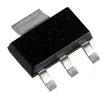
Power MOSFET, N Channel, 400 V, 500 mA, 2.2 ohm, SOT-223, Surface Mount
- Manufacturer: INFINEON
- Product type: Single MOSFETs
- Channel Type: N Channel
- Power Dissipation: 1.8W
- Drain Source On State Resistance: 2.2ohm
| Delivery and price | |
|---|---|
| Units per pack | 1000 |
| Price | 0.298 € |
| Current stock | 10+ |
| Lead time | 30 days |
**BSP298** ## **SIPMOS[ ®] Small-Signal Transistor** - N channel - Enhancement mode - Avalanche rated - _V_ = 2.1 ... 4.0 V GS(th) - Pb-free lead plating; RoHS compliant - Qualified according to AEC Q101 • Halogenfree according to IEC61249221 aa 1 Pin 1 Pin 2 Pin 3 Pin 4 G D S D source pin3 +++ |**Type**|**_V_DS**|**_I_D**|**_R_DS(on)**|**Package**||**Marking**| |---|---|---|---|---|---|---| |BSP298|400 V|0.5 A|3Ω|PG-SOT223||BSP298| |||||||| |**Type**|**Pb-free**||**Tape and Reel Information**||**Packaging**|| |BSP298|Yes||H6327||Dry|| ## **Maximum Ratings** |**Maximum Ratings**|||| |---|---|---|---| |**Parameter**|**Symbol**|**Values**|**Unit**| |Continuous drain current<br>_T_A= 26 °C|_I_D|0.5|A| |DC drain current, pulsed<br>_T_A= 25 °C|_I_Dpuls|2|| |Avalanche energy, single pulse<br>_I_D= 1.35 A,_V_DD= 50 V,_R_GS= 25Ω<br>_L_= 125 mH,_T_j= 25 °C|_E_AS|130|mJ| |Gate source voltage|_V_GS|±20|V| |Power dissipation<br>_T_A= 25 °C|_P_tot|1.8|W| |ESD Class<br>JESD22-A114-HBM||Class 1b|| 2012-11-29 Rev. 2.6 1 **BSP298** ## **Maximum Ratings** |**Parameter**|**Symbol**<br>ee<br>ee|**Values**<br>ee<br>eee|**Unit**<br>ee<br>eee| |---|---|---|---| |Chip or operating temperature|_T_j<br>ee<br>ee<br>ee|-55 ... + 150<br>ee<br>eee<br>eee|°C<br>ee<br>eee<br>eee<br>eee| |Storage temperature|_T_stg<br>ee <br>ee<br>ee|-55 ... + 150<br> eee<br>eee<br>eee|| |Thermal resistance, chip to ambient air|_R_thJA<br>ee <br>ee|≤70<br> eee<br>eee|K/W<br>eee<br>eee<br>eee| |Therminal resistance, junction-soldering point1)|_R_thJS<br>ee <br>a <br>ee|≤10<br> eee<br> eee<br>eee|| |DIN humidity category, DIN 40 040|ee<br>ee|E<br>eee<br>ee|eee<br>ee| |IEC climatic category, DIN IEC 68-1|ee <br>ee|55 / 150 / 56<br> eee<br>ee|| 1) Transistor on epoxy pcb 40 mm x 40 mm x 1,5 mm with 6 cm[2] copper area for drain connection |Drain- source breakdown voltage<br>_V_GS= 0 V,_I_D= 0.25 mA,_T_j= 0 °C|_V_(BR)DSS<br>~~|~~|400<br>~~|~~<br>~~|~~|-<br>~~|~~<br>~~|~~|-<br>~~|~~<br>~~|~~|V<br>~~|~~<br>~~|~~| |---|---|---|---|---|---| |Gate threshold voltage<br>_V_GS=_V_DS,_I_D= 1 mA|_V_GS(th)|2.1<br>~~|~~|3<br>~~|~~|4<br>~~|~~|| |Zero gate voltage drain current<br>_V_DS= 400 V,_V_GS= 0 V,_T_j= 25 °C<br>_V_DS= 400 V,_V_GS= 0 V,_T_j= 125 °C|_I_DSS|-<br>-<br>||10<br>0.1<br>|||100<br>1<br>||µA| |Gate-source leakage current<br>_V_GS= 20 V,_V_DS= 0 V|_I_GSS<br>||-<br>|<br>|<br>||10<br>|<br>||<br>||100<br>|<br>||nA| |Drain-Source on-state resistance<br>_V_GS= 10 V,_I_D= 0.5 A|_R_DS(on)<br>||-<br>|<br>|<br>||2.2<br>| |<br>|<br>||3<br>|<br>||Ω| 2012-11-29 Rev. 2.6 2 **BSP298** > **Electrical Characteristics,** at _T_ j = 25°C, unless otherwise specified |Transconductance<br>_V_DS≥2*_I_D *_R_DS(on)max,_I_D= 0.5 A|_g_fs<br>~~|~~|0.5<br>~~|~~<br>|<br>||1.2<br>~~|~~<br>|<br>|||-<br>~~|~~<br>||S| |---|---|---|---|---|---| |Input capacitance<br>_V_GS= 0 V,_V_DS= 25 V,_f_= 1 MHz|_C_iss<br>ef|-<br>|<br>ef<br>|<br>||300<br>|<br>ef<br>||<br>||400<br>ef<br>||pF| |Output capacitance<br>_V_GS= 0 V,_V_DS= 25 V,_f_= 1 MHz|_C_oss<br>||-<br>|<br>|<br>||50<br>| |<br>|<br>||75<br>|<br>||| |Reverse transfer capacitance<br>_V_GS= 0 V,_V_DS= 25 V,_f_= 1 MHz|_C_rss|-<br>||20<br>||30|| |Turn-on delay time<br>_V_DD= 30 V,_V_GS= 10 V,_I_D= 0.3 A<br>_R_GS= 50Ω|_t_d(on)|-|10|15|ns| |Rise time|_t_r||||| ||||||| |||-|25|40|| ||_t_d(off)||||| ||||||| |||-|30|40|| ||_t_f||||| ||||||| |||-|20|30|| 3 2012-11-2 Rev. 2.6 **BSP298** > **Electrical Characteristics,** at _T_ j = 25°C, unless otherwise specified |Inverse diode continuous forward current<br>_T_A= 25 °C|_I_S<br>~~|~~|-<br>~~|~~<br>||-<br>~~|~~<br>||0.5<br>~~|~~|A| |---|---|---|---|---|---| |Inverse diode direct current,pulsed<br>_T_A= 25 °C|_I_SM<br>eT|-<br>|<br>eT<br>||-<br>|<br>eT<br>||2<br>eT|| |Inverse diode forward voltage<br>_V_GS= 0 V,_I_F= 1 A,_T_j= 25 °C|_V_SD<br>ef]|-<br>ef]<br>||0.95<br>ef]<br>||1.2<br>ef]|V| |Reverse recovery time<br>_V_R= 100 V,_I_F=_l_S,d_i_F/d_t_= 100 A/µs|_t_rr<br>ef]|-<br>|<br>ef]|300<br>|<br>ef]|-<br>ef]|ns| |Reverse recovery charge<br>_V_R= 100 V,_I_F=_l_S,d_i_F/d_t_= 100 A/µs|_Q_rr<br>et|-<br>et|2.5<br>et|-<br>et|µC| 4 2012-11-29 Rev. 2.6 **BSP298** ## **Power dissipation** _P_ tot = ƒ( _T_ A) ## **Drain current** _I_ D = ƒ( _T_ A) parameter: _V_ GS ≥ 10 V **==> picture [486 x 259] intentionally omitted <==** **----- Start of picture text -----**<br> 2.0 A 0.55<br>W BERRPrIN] |] tty ey yy yy A PLING TEELELLLLLL<br>P 1.6 PEE NET ET ET ee yt I 0.45 ~<<br>tot D<br>Soun VoeSane<br>0.40<br>1.4 PTT TIN; | Ey ey yySeeyy ee SOREX<br>COCEE REE rrr ALELEE<br>0.35<br>1.2 FEEEEENSEEEE LEN LLL<br>PET EEE 0.30 EELTLLLENELEE<br>1.0 PT TET INANE ET ET ETT I \<br>PT tTTT tTetETtT] INAPTET T TTyy 0.25 TTL EAT \NEE<br>PE<br>0.8<br>PT tT tT Ee tT TIN | TT yy 0.20<br>0.6 Po eee<br>0.15<br>Fit ttt ttt tT TAT ETT<br>0.4 SSS00000000K 0008 LEELA<br>BERR 0.10 \<br>0.2 SERENE 0.05<br>0.0 0.00<br>PET ET EET ET ET TIN | |<br>0 PE 20 40 60 80 100 E 120 °C 160 = 0 C 20 40 60 80 r 100 120 °C 160<br>— T A — T A<br>**----- End of picture text -----**<br> **Safe operating area** _I_ D=f( _V_ DS) parameter : _D_ = 0, _T_ C=25°C ## **Transient thermal impedance** _Z_ th JA = ƒ( _t_ p) parameter: _D = t_ / _T_ p **==> picture [237 x 264] intentionally omitted <==** **----- Start of picture text -----**<br> 10 2<br>K/W<br>10 1 ee, a ENE NEE NN LIE<br>Z Seemetetteteteetttrmeentt= TT | | aa | tT<br>thJC [LTT NATIT TDRUE TEI TET [Tea<br>10 0<br>10 -1<br>aSUSE<br>D = 0.50<br>10 -2<br>0.20<br>0.10<br>Sti oralmemati<br>10 -3 7Anth 0.05 Se<br>single pulse 0.02<br>10 -4 VA ll 0.01<br>Sei seat at seat sot sav sat we<br>10 -5 ECA CCAPC<br>-8 -7 -6 -5 -4 -3 -2 -1 0<br>10 10 10 10 10 10 10 10 s 10<br>— t<br>p<br>**----- End of picture text -----**<br> 2012-11-29 5 Rev. 2.6 **BSP298** ## **Typ. output characteristics** _I_ D = ƒ( _V_ DS) parameter: _t_ p = 80 µs , _T_ j = 25 °C ## **Typ. drain-source on-resistance** _R_ DS (on) = ƒ( _I_ D) parameter: _t_ p = 80 µs, _T_ j = 25 °C **==> picture [485 x 269] intentionally omitted <==** **----- Start of picture text -----**<br> l<br>1.2 10<br>P tot = 2W j<br>A kgc ihe d f b Ω a<br>1.0 V GS [V]<br>I a 4.0 R 8<br>D yy DS (on) LEE<br>0.9 b 4.5<br>c 5.0 7<br>0.8<br>d 5.5<br>0.7 e 6.0 6<br>THY TTT tert<br>f 6.5<br>PALL aoeLLL<br>0.6 g 7.0 5<br>h 7.5<br>0.5 ffs a i 8.0 4 TELE<br>b<br>j 9.0<br>0.4<br>k 10.0 3 eT<br>0.3 HANEY l 20.0 E ye<br>l jh d figcke<br>2<br>0.2<br>V GS [V] =<br>0.1 1 a b c d e f g h i j k l<br>4.0 4.5 5.0 5.5 6.0 6.5 7.0 7.5 8.0 9.0 10.0 20.0<br>0.0 Po 0 AL<br>Pili [littl] i td<br>0 1 2 3 4 5 6 7 8 V 10 0.00 0.10 0.20 0.30 0.40 A 0.60<br>V I<br>DS D<br>**----- End of picture text -----**<br> Typ. transfer characteristics _I_ D _= f_ ( _V_ GS) parameter: _t_ p = 80 µs Typ. forward transconductance _g_ fs = _f_ ( _I_ D) parameter: _t_ p = 80 µs, **==> picture [228 x 257] intentionally omitted <==** **----- Start of picture text -----**<br> 2.6<br>A PLT TTT TTT<br>2.2 ete tt ty Ey<br>I<br>D 2.0 PLT tT TT ET<br>Seis<br>1.8<br>1.6 Pt<br>1.4 Pt TT T ATT yyTT<br>1.2 ett tT UE TT Ed<br>1.0 Pt tT yy Ty yt<br>0.8 tt<br>0.6 |i t eeu |TTT ey<br>0.4 PLT TP et tt to<br>0.2 tet<br>0.0<br>PLT ULE ft tT T TEyLo<br>0 1 2 3 4 5 6 7 8 V 10<br>V<br>GS<br>**----- End of picture text -----**<br> **==> picture [230 x 257] intentionally omitted <==** **----- Start of picture text -----**<br> 2.6<br>S Pt tt ey | yt<br>2.2 Pt tT ET | eT<br>g fs 2.0 Seas<br>PTET<br>1.8<br>1.6 Ey TT Td<br>1.4 P TLLttyYL_ ET T ETet te<br>1.2 PL YET ET EL ty<br>1.0 FIAT<br>0.8 ET TET te<br>0.6 AePALIT<br>0.4 ALT TT E TttTET<br>0.2 ttt<br>0.0 TELL<br>AP LE TET T T | td<br>0.0 0.4 0.8 1.2 1.6 A 2.2<br>I<br>D<br>**----- End of picture text -----**<br> 6 2012-11-29 Rev. 2.6 **BSP298** ## **Drain-source on-resistance** _R_ DS (on) = ƒ( _T_ j) ## parameter: _I_ D = 0.5 A, _V_ GS = 10 V ## **Gate threshold voltage** _V_ GS (th) = ƒ( _T_ j) parameter: _V_ GS = _V_ DS, _I_ D = 1 mA **==> picture [489 x 258] intentionally omitted <==** **----- Start of picture text -----**<br> 7.5 4.6<br>Ω V<br>98%<br>6.5 PEEP EPP ee 4.0 ee eo<br>R 6.0 Pit tT tT Ey Et V a<br>DS (on) GS(th) 3.6<br>5.5<br>Pi; tT ty ee ey ty a<br>3.2 typ<br>5.0<br>FEE fo SRE<br>4.5 Pt ttt te et et 2.8 a<br>4.0<br>pt tt ty 98% tet | 2.4 ee 2%<br>3.5<br>POPC ere Eee<br>2.0<br>3.0 Pt | | feet typ [oer | a<br>2.5 1.6<br>Coe ert Eee ee<br>2.0 pt | ee tt 1.2 a<br>1.5 +7) | | | tt tt |<br>0.8<br>1.0 Pi Tey Ee a<br>0.4<br>0.5 Pit tT tT Ey Et So<br>0.0 0.0<br>Pit} eet tt tt a<br>-60 -20 20 60 100 °C 160 -60 -20 20 60 100 °C 160<br>T T<br>j j<br>**----- End of picture text -----**<br> ## **Typ. capacitances** _C_ = _f_ ( _V_ DS) parameter: _V_ GS=0V, _f_ = 1 MHz ## **Forward characteristics of reverse diode** _I_ F = ƒ( _V_ SD) parameter: _T_ j _, t_ p = 80 µs **==> picture [227 x 261] intentionally omitted <==** **----- Start of picture text -----**<br> 10 1<br>===<br>nF a<br>C<br>Pot<br>| ft<br>10 0<br>eee<br>ee C<br>a a a iss<br>10 -1<br>NRE<br>C<br>——— oss<br>a a<br>C<br>rss<br>10 -2 CEES<br>0 5 10 15 20 25 30 V 40<br>V<br>DS<br>**----- End of picture text -----**<br> **==> picture [226 x 263] intentionally omitted <==** **----- Start of picture text -----**<br> 10 1<br>EEE EERE<br>A EEE EEE<br>I<br>F a<br>SESE ER ES SeEeeee<br>10 0<br>eeta<br>ECO<br>TAP<br>10 -1<br>oe tf<br>T j = 25 °C typ<br>fe T j = 150 °C typ ==<br>EIS T j = 25 °C (98%) qc<br>T j = 150 °C (98%)<br>10 -2 =O or<br>0.0 0.4 0.8 1.2 1.6 2.0 2.4 V 3.0<br>V<br>SD<br>**----- End of picture text -----**<br> 7 2012-11-29 Rev. 2.6 **BSP298** ## **Avalanche energy** _E_ AS = ƒ( _T_ j) parameter: _I_ D = 1.35 A, _V_ DD = 50 V _R_ GS = 25 Ω, _L_ = 125 mH ## **Drain-source breakdown voltage** _V_ (BR)DSS = ƒ( _T_ j) **==> picture [484 x 260] intentionally omitted <==** **----- Start of picture text -----**<br> 140 480<br>mJ REREReee V PT EET ELE<br>REE LLL<br>120 PTT<br>460<br>E AS 110 PAL ETT ETE EE V (BR)DSS TTPTyr<br>450<br>100<br>PINT TE EEL TL Seen<br>440<br>90<br>PCR ff ppp<br>430<br>80<br>PILING TE EET oie<br>70 420<br>PTT AEE TT ET Ty tI titi t ty<br>60 PLT TREE ETE 410 PT LET<br>50 PTTL INGE FEEL EL PT] LYELL<br>400<br>PLT ELE<br>40<br>TEIN EEE TTA<br>390<br>30<br>PTTL EE NEEL EL TVET EELLL<br>380<br>20<br>PTTL TTT ING ET ET ETT<br>10 PTT TTT TT PN UE TTI 370 /<br>0 360<br>PL TT EE EE ELA FELT EEEL ELLE<br>20 40 60 80 100 120 °C 160 -60 -20 20 60 100 °C 160<br>— T j — T j<br>**----- End of picture text -----**<br> **Safe operating area** _I_ D=f( _V_ DS) parameter : _D_ = 0.01, _T_ C=25°C 8 2012-11-29 Rev. 2.6 **BSP298** ## **Package outlines** SOT-223 Dimensions in mm 9 2012-11-29 Rev. 2.6 **BSP298** 10 Rev. 2.6 2012-11-29
Updated at February 9, 2023
Infineon Technologies is a globally recognized leader in semiconductor solutions, renowned for driving innovation in power management, energy efficiency, and modern mobility. With a strong legacy of engineering excellence, the company provides highly reliable components designed to meet the rigorous demands of industrial, automotive, and advanced commercial applications. The core of our Infineon portfolio is centered on their industry-leading discrete semiconductors. We offer an extensive selection of single and dual MOSFETs, alongside a robust range of single IGBTs and advanced IGBT modules. These flagship power transistors are essential for high-efficiency power conversion and motor control, providing engineers with superior thermal performance and minimized switching losses. Beyond advanced field-effect transistors, the selection includes a comprehensive array of diodes and rectifiers, heavily featuring Schottky diodes, as well as fast-recovery and RF/PIN diodes. This power foundation is further supported by bipolar transistors, intelligent power modules, and thyristor SCR modules, delivering the critical building blocks required for complex power system designs. To support broader system integration, the portfolio also encompasses specialized solutions such as solid-state relays, AC/DC LED driver ICs, and Bluetooth communications modules. From high-power industrial rectifiers to wireless connectivity adapters, Infineon equips designers with the precision components needed to build efficient, scalable, and fully connected electronic systems.
About Novapart
Novapart is a B2B electronic component broker specialising in stock shortages and cost reduction. We source hard-to-find parts and identify compliant alternatives across a catalogue of 410,000+ components from 500+ manufacturers.
Learn more →Stock Shortage Specialist
When a component is unavailable, discontinued or has an unacceptable lead time, we tap into our network of vetted European and Asian distributors to source what you need — without compromising on quality or traceability.
Request a quote →Compliant Alternatives
We identify pin-to-pin, electrically equivalent substitutes that meet the same certifications (RoHS, AEC-Q100, REACH) as your original specification — validated against datasheets, not just part numbers. Often at a lower cost.
BOM Analysis service →