


BSP135IXTSA1
Power MOSFET, N Channel, 600 V, 120 mA, 45 ohm, SOT-223, Surface Mount
- Manufacturer: INFINEON
- Product type: Single MOSFETs
- MSL: MSL 1 - Unlimited
- SVHC: No SVHC (25-Jun-2025)
- No. of Pins: 4Pins
- Channel Type: N Channel
- Product Range: -
- Qualification: -
- Power Dissipation: 1.8W
- Transistor Mounting: Surface Mount
- Rds(on) Test Voltage: 10V
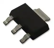
- Transistor Case Style: SOT-223
- Drain Source Voltage Vds: 600V
- Operating Temperature Max: 150°C
- Continuous Drain Current Id: 120mA
- Drain Source On State Resistance: 45ohm
- Gate Source Threshold Voltage Max: 1.4V
| Delivery and price | |
|---|---|
| Units per pack | 500 |
| Price | 0.194 € |
| Current stock | 500+ |
| Lead time | 7 days |
BSP135I

**==> picture [109 x 43] intentionally omitted <==**

**----- Start of picture text -----**<br>
a<br>Cinfineone@<br>**----- End of picture text -----**<br>


## Small ~~-S~~ ignal Transistor

## Features

¢ N ~~-~~ channel

- Depletion mode

¢ dv/dt rated

¢ Halogen ~~-f~~ ree according to IEC61249 ~~-2-2~~ 1 * Pb ~~-f~~ ree lead plating; ROHS compliant

## Product validation

**==> picture [95 x 120] intentionally omitted <==**

**----- Start of picture text -----**<br>
SOT -2 23 -4<br>4<br>3<br>&<br>N<br>&<br>2<br>°<br>**----- End of picture text -----**<br>


Fully qualified according to JEDEC for Industrial Applications

## ~~Table 1 Key Performance Parameters~~

ESD Sensitivity, Class1A JESD22-A114 (HBM) |(>250V,<500V)

**==> picture [18 x 14] intentionally omitted <==**

**----- Start of picture text -----**<br>
P in d<br>**----- End of picture text -----**<br>


**==> picture [37 x 40] intentionally omitted <==**

**----- Start of picture text -----**<br>
(6)<br>**----- End of picture text -----**<br>


**==> picture [83 x 36] intentionally omitted <==**

**----- Start of picture text -----**<br>
@ ROHS<br>**----- End of picture text -----**<br>


~~BSP135 PG-SOT223~~

~~SP1351~~

**==> picture [127 x 19] intentionally omitted <==**

**----- Start of picture text -----**<br>
Pe<br>**----- End of picture text -----**<br>


Final Data Sheet

1

Rev ~~.~~ 2 ~~.~~ 1, 2021 ~~-0~~ 3 ~~-~~ 16

**==> picture [121 x 53] intentionally omitted <==**

**==> picture [167 x 165] intentionally omitted <==**

~~OT~~

## Small ~~-S~~ ignal ~~BSP135l Transistor~~

**==> picture [120 x 56] intentionally omitted <==**

**----- Start of picture text -----**<br>
Tnfit<br>C in neon ;<br>**----- End of picture text -----**<br>


1 Maximum ratings at Ta=25 °C, unless otherwise specified

**==> picture [542 x 366] intentionally omitted <==**

**----- Start of picture text -----**<br>
Table 2_—/ Maximum ratings<br>m aramet er Symbol,ymbo Min. |aeTyp. [Max._it Noote /| TeTe t s t ConditionCondit<br>Continuous drain current » Ff er ae C<br>j,max—<br>Reverse diode dvidt dvidt - be | kVius |12-0-12 2 1Gs=20 V, dildit=200 Alus,<br>Se oe<br>2 Thermal characteristics<br>Table 3_— Thermal characteristics<br>p aramet er symbol,ymbo Min. _|aeTyp. [Max._nit N o te /I TeTe t s t ConditionCondit<br>Thermal resistance, junction - soldering<br>oa mbm<br>SMD version, device on PCB, bw<br>SMD version, device on PCB,<br>**----- End of picture text -----**<br>


## 3 Electrical characteristics

at Tj=25 °C, unless otherwise specified

## Table 4 Static characteristics

|Table 4|Static characteristics|characteristics|characteristics|characteristics|characteristics|characteristics|characteristics|characteristics|characteristics|
|---|---|---|---|---|---|---|---|---|---|
|~~p~~~~**aramet**~~<br>~~Sym~~<br>~~er~~<br>~~Drain-sourcebreakdownvoltage~~<br>~~[Veross~~||||~~Sym~~~~**bo**ljae~~<br>~~ym~~<br>~~Min.~~<br>~~[Veross~~<br>~~[600~~|~~jae~~<br>~~Min._|~~<br>~~Typ.[Max._~~|||~~it~~<br>~~|v|~~|~~N~~~~**o**|Te~~~~**s**t~~<br>~~Condit~~<br>~~te /Te t~~<br>~~Condition~~<br>~~Ves=-3V,[p=250UA~~|
||||||~~jae~~<br>~~Min._|~~<br>~~Typ.~~<br>~~[600|-~~|~~jae~~<br>~~_|~~<br>~~Typ.[Max._~~<br>~~|-~~<br>~~|-~~|~~[Max._~~<br>~~|-~~<br>~~|v~~|||
|~~p~~~~**aramet**~~<br>~~Sym~~<br>~~er~~<br>~~Drain-sourcebreakdownvoltage~~<br>~~[Veross~~||||~~Sym~~~~**bo**l jae~~<br>~~ym~~<br>~~Min.~~<br>~~[Veross~~<br>~~[600~~|~~jae~~<br>~~Min._|~~<br>~~Typ.~~<br>~~[600|-~~|~~jae~~<br>~~_|~~<br>~~Typ. [Max._~~<br>~~|-~~<br>~~|-~~|~~[Max._~~<br>~~|-~~<br>~~|v~~|~~it ~~<br>~~|v|~~|~~N~~~~**o** | Te~~~~**s**t~~<br>~~Condit~~<br>~~te / Te t~~<br>~~Condition~~<br>~~Ves=-3V,[p=250UA~~|
|~~Drain-source breakdown voltage~~<br>~~[Veross~~<br>Gate threshold voltage||||~~[Veross~~<br>~~[600~~|~~[600 |-~~|~~|-~~<br>~~|-~~|~~|-~~<br>~~|v~~|~~|v | ~~|~~Ves=-3 V, [p=250 UA~~<br>Vos=3 V, Ip=94 UA|
|Drain~~-~~source cutoffcurrent<br>~~a~~<br>~~Gate-sourceleakagecurrent~~<br>~~ess~~||||~~a~~<br>~~ess~~<br>~~ese~~|~~ese~~|~~ese~~|~~9~~<br>~~100[nA~~|~~[nA~~|Ve=600vVie~~ns~~veianSo<br>=<br>,<br>Ves=-3<br>V,<br>T=<br>~~Ves=20V,Vos=0V~~|
|~~Gate-sourceleakagecurrent~~<br>~~ess~~<br>~~On-statedraincurrent~~<br>~~loss~~||||~~ess~~<br>~~ese~~<br>~~lossSsf20s~~|~~ese~~<br>~~f20s|e~~|~~ese~~<br>~~|e~~<br>~~>~~|~~100[nA~~|~~[nA~~<br>~~ma~~|~~Ves=20V,Vos=0V~~<br>~~Ves=0V,Vos=10V~~|
|~~Gate-source leakage current~~<br>~~ess~~<br>~~On-statedraincurrent~~<br>~~loss~~<br>~~Drain-sourceon-stateresistance~~<br>~~osm~~||||~~ess~~<br>~~ese~~<br>~~lossSsf20s~~<br>~~osm~~|~~ese~~<br>~~f20s|e~~<br>~~|~~|~~ese~~<br>~~|e~~<br>~~>~~<br>~~3~~|~~100 [nA~~<br>~~°°~~|~~[nA ~~<br>~~ma~~|~~Ves=20 V, Vos=0 V~~<br>~~Ves=0V,Vos=10V~~<br>~~VeetOV.aneA~~|
|~~On-state drain current~~<br>~~loss~~<br>~~Drain-sourceon-stateresistance~~<br>~~osm~~<br>~~Transconductance~~<br>~~las~~||||~~loss Ss f20s~~<br>~~osm~~<br>~~las~~<br>~~-—'fo.o8.~~|~~f20s |e~~<br>~~|~~<br>~~-—'fo.o8.ote~~|~~|e~~<br>~~>~~<br>~~3~~<br>~~ote|-~~|~~°°~~<br>~~|-~~<br>~~|s~~|~~ma ~~<br>~~|s|~~|~~Ves=0 V, Vos=10 V~~<br>~~VeetOV.aneA~~<br>~~|Vos|>2|!p|Ros(on)max,[>=0.1A~~|
|~~Drain-source on-state resistance~~<br>~~osm~~<br>~~Transconductance~~<br>~~las~~||||~~osm ~~<br>~~las~~<br>~~-—'fo.o8.~~|~~|~~<br>~~-—'fo.o8.ote~~|~~3~~<br>~~ote|-~~|~~°°~~<br>~~|-~~<br>~~|s~~|~~|s|~~|~~VeetOV.aneA~~<br>~~|Vos|>2|!p|Ros(on)max,[>=0.1A~~|


*) Device on 40 mm x 40 mm x 1.5 mm epoxy PCB FR4 with 6 cm? (single layer, 70 um thick) copper area for Final Data Sheet 3

Rev ~~.~~ 2 ~~.~~ 1, 2021 ~~-0~~ 3 ~~-~~ 16

Small ~~-S~~ ignal Transistor

BSP135l

**==> picture [120 x 45] intentionally omitted <==**

**----- Start of picture text -----**<br>
om<br>e@<br>Cinfi neon ;<br>**----- End of picture text -----**<br>


**==> picture [539 x 490] intentionally omitted <==**

**----- Start of picture text -----**<br>
||||||||||||||||||
|---|---|---|---|---|---|---|---|---|---|---|---|---|---|---|---|---|
|Table|5|Dynamic|characteristics|
|arameter|ymbo|Min.|_|Typ.||Max._||ote /|Test|Condition|
|Input|capacitance|css|fe|98|[|p|Ves=-3|V,|Vos=25|V,|1|MHz|
|Output|capacitance|Coss|ses]|Ves=-3|V,|Vos=25|V,|1|MHz|
|Reverse|transfer|capacitance|Ces|ses|Ves=-3|V,|Vos=25|V,|F1|MHz|
|.|Vop=300|V,|Ves|=-|3to|5|V,|Ip=0|.|1|A,|
|wg|Vop=300|V,|Ves=|-|3|to|5|V,|Ip=0|.|1|A,|
|:|Vop=300|V,|Ves=|-|3|to5|V,|lp=0|.|1|A,|
|F|Vop=300|V,|Ves=|-|3|to|5|V,|/p=0|.|1|A,|
|Table|6|Gate|charge|characteristics|
|m|aramet|er|Symym|bo|l|jaeMin.||Typ.|[Max._|it|N|o|te /||TeTe t|s|t|ConditionCondit|
|Gate|to|source|charge|las|ides|fe|[nc|Vpp=400|V,|/b=0.1|A,|Ves=-3|to|5|V|
|Gate|to|drain|charge|las|=|ses.|fe|[nc|Voo=400|V,|/p=0.1|A,|Ves=-3|to|5|V|
|Gate|charge|total|la,|fe|8.7|||[nC]|Von|=400|V,|1020.1|A,|Vos=-3|to|5|V|
|Gate|plateau|voltage|Vpiteau|||——*0.20||-|——|V—|||Von=400|V,|/n=0.1|A,|Vos=-3|to|5|V|
|Table|7|Reverse|diode|
|p|aramet|er|Symbol,ymbo|Min.||eae|lumote /I|TeTe t|s|t|ConditionCondit|
|Typ.||Max.|
|Diode|continous|forward|current|a|ee|eee|Ta=25|°C|
|Diode|forward|voltage|Veo||=|*f0.78||4.2|[V__|||Vos=-3|V,|Ir=0.12|A,|Ti=25|°C|
|Reverse|recovery|time|tt||-———«|87—«4(130ns|Va=300|V,|Ir=0.1|A,|dir/dt=100|Alys|
|Reverse|recovery|charge|la,|ses||70|104|[nc|Vr=300|V,|Ir=0.1|A,|dir/df=100|A/us|

**----- End of picture text -----**<br>


Final Data Sheet

4

Rev ~~.~~ 2 ~~.~~ 1, 2021 ~~-0~~ 3 ~~-~~ 16

on Cinfi neon }

Small ~~-S~~ ignal Transistor BSP135l

## 4 Electrical characteristics diagrams

**==> picture [527 x 620] intentionally omitted <==**

**----- Start of picture text -----**<br>
2.0 0.14<br>—P t yf | ty dl SERRE<br>S INCE mot tit tte etEE<br>\<br>" EINE | EERE<br> | EEE<br>= CONC or<br>io z iit tt A<br>PENT PEN<br>05 CEE NTEX P tttES<br>PEL Ey EEE<br>ET PNT YY e ePPE<br>ot LL [LEN] \ eee<br>0 40 80 120 160 0 20 40 60 80 100 120 140 160<br>Ta [°C] Ta [°C]<br>10°  eo ooo ooo 102<br>SS eee a<br>TT ANT Troduel fT ae ae<br>CENT CHINN TAIT ST TE cae Tit<br>L LM TINT | ITCH<br>SSA cee ATTT<br>Ss 02tL it<br>— 1 Pall L Le<br>i , ZY VI LINE ET a C eoe oe CEH<br>a ee ee<br>eat eee 0,024 Pee TE TET<br>EELT TT TTT esTTTtNhe ATTTt AgenAN CLINI EUIM ULIaETM [ul<br>o e +rote)LEU LUI EI PUNT TUTTI TT<br>10° 10' 10? 10° 10 4 10 ° 10 ? 10 " 10° 10' 10?<br>Vos [V] t [s]<br>**----- End of picture text -----**<br>


Final Data Sheet

5

Rev ~~.~~ 2 ~~.~~ 1, 2021 ~~-0~~ 3 ~~-~~ 16

~~BSP135l ee~~

## Small ~~-S~~ ignal[Transistor]

**==> picture [93 x 42] intentionally omitted <==**

**----- Start of picture text -----**<br>
\ [<n]<br>infin neon<br>**----- End of picture text -----**<br>


**==> picture [530 x 651] intentionally omitted <==**

**----- Start of picture text -----**<br>
Diagram 5: Typ. output characteristics Diagram 6: Typ . drai n- source on resistance<br>0.25 100<br>ew /<br>Yay | | t ev fod fea | te v)<br>LP<br>ERY Zee E ER<br>0.15 aoe A, Aeee 60 EPP<br>ce Wi ||| fg Titty yy<br>0 /JZ es a<br>|{= |<br>0.05 _) Anne p ary ==———e—E—EeEeee<br>y/ lr 20 a a a<br>m v taa a Eas<br>0 2 TE4  LTT6 8TTT}10 0 .E 00 E T 0 . 04 E0 E. 08T 0 . 12T E 0 . 16 0 . 20<br>Vos [V] bb [A]<br>Ip=f(Vos), T7=25 °C; parameter: Ves Rosvon)=f(/p), T=25 °C; parameter: Ves<br>Diagram 7: Typ. transfer characteristics Diagram 8: Typ . transconductance<br>e e 9 . 20<br>a A<br>SESS eps eff<br>ee ee eee ee ra<br>0 2 Sel 0} p06GG A ra<br>a ee eee ee ee 0 . 15 7<br>eeee eee ee<br>eeee ee) ee<br>oi | | | | | | | | T/ey fl<br>z BI| | | | CU |G WA<br>= | | | ttA tl 4<br>& — | | | | | | | Tf lh Uf<br>oro | | | t | | | TAT | |<br>“L t | | | | | Yt 7 ft<br>eeeee eee<br>ee| eee eee<br>| | | | | yf” | | 0.05<br>oo | | | | | [fy | | | |<br>“LE | | ft | | Y7L | fT tT ft<br>ee— ee ee ee ee eee<br>| | | | ¥yA_ | | | ll<br>000 -—ee 0.00<br>- 2.0 - 1 . 5 - 1 . 0 - 0.5 0.0 0.5 1.0 0.00 0.04 0.08 0 . 12<br>Ves [V] Ip [A]<br>Ib=f(Ves), |Vos|>2|/o|Ros(onymax; parameter: T; Gis=f(Ip)<br>**----- End of picture text -----**<br>


Final Data Sheet

6

Rev ~~.~~ 2 ~~.~~ 1, 2021 ~~-0~~ 3 ~~-~~ 16

BSP1351

## Small ~~-S~~ ignal[Transistor]

**==> picture [94 x 41] intentionally omitted <==**

**----- Start of picture text -----**<br>
e_—<br>In fineon<br>**----- End of picture text -----**<br>


**==> picture [528 x 651] intentionally omitted <==**

**----- Start of picture text -----**<br>
Diagram 9: Normalized drai n- source on resistance Diagram 10: Typ . gate threshold voltage<br>2.5 TLITLTTLILTLLLLILILILLILILILILLL 0.0 SO<br>EEEEEEEEEE Ee po  RSS<br>Pt tt tt A A<br>6 2 EERE]PITT TPE Tre rey ee ee ye | [E] ee a a [RE] ERE EEE<br>OS Se(CLITTT tT tri t tt Att pea<br>FECES) R SE<br>0 45 Z SS rr<br>*~ "TELE ETTE Ae aOO<br>Bee fe<br>es HHA 8 ere<br>e6 fLitTttTTiiT tT tT TT wit t iit t ttt) 3 a<br>2= Caiottt Tt TT eT TT TTT TT | |YS Jaeee<br>ge VV -2.0<br>& COO SSSSSSSE EE<br>oe PitrPFPEPHEEL Pr ee eeerereeeEEEEE ET Et | 2a57-7 oeesSSE<br>SSCL “ec a<br>PET TTT TT PT tT et aSOOO<br>oo  LOCA 39  Pett<br>- 80 - 40 0 40 80 120 160 - 60 - 20 20 60 100 140 180<br>TEC] nC)<br>Rosion)=f(7}), Ip=0.01 A, Ves=0 V V Vesithy=f(7}), Vos=3 V; Ip=94 yA<br>Diagram 11: Typ. capacitances Diagram 12: Forward characteristics of reverse diode<br>10°  (ERE 3 100 (SS<br>Arte teteA TTT tT tee tt eette te te te tt tt tt |[}—-—25°C,max° ee[] yy ee eee ee<br>COC J---i50°¢) OE<br>NTE | | |<br>PeetSS | R e ese<br>SONIC ATAU<br>10° eee Aeee 10 SS SS SS AS FS<br>A A e e SS RS A A Ss<br>A SS RS A A PR |<br>ee eee a a a | ee ee ee ee<br>gE2. \ fga Eeql<br>a Xe<br>ESET LE Ee<br>eee a | YS<br>A ee ee a SS|<br>FEC EEE rss a<br>LTT TTT TT eT TTT TTT TE | Pre nn eee<br>PLETE EEE EEE PTT cdi Tg ta PT TT TT<br>e ALLELE)0 5 10 15 20 25 .  LA0.0 0.2 0.4 Ee0.6 0.8 1.0 EE P1 . 2 1 . 4 1 . 6<br>Vos [V] Vsp [V]<br>C=f(Vps); Ves= - 3 V; 1 MHz l=f(Vsp), Ves= - 3 V; parameter: T;<br>**----- End of picture text -----**<br>


Rosion)=f(7}), Ip=0.01 A, Ves=0 V V

Final Data Sheet

7

Rev ~~.~~ 2 ~~.~~ 1, 2021 ~~-0~~ 3 ~~-~~ 16

on Cinfineon ; ~~Te~~

Small ~~-S~~ ignal Transistor ~~BSP1351~~

**==> picture [527 x 268] intentionally omitted <==**

**----- Start of picture text -----**<br>
10a —E s eee-——————— 680 ALE EEE EEE<br>T T } ] tT ye tr FUELEE EP<br>Pe e See e eyGee<br> eee AULTEET EE<br>Ss aae eeAne<br>a | | | | Ye | Ee<br>AP ee<br>tityet tt tT te UPA<br>pee | | | EEE<br>ft | | | | | ft tf ULEEEE EEE<br>2  pti i ft |} ft tf ott lA tT TTTTT<br>P| | | | | cf | Tf ALLELEEL EEEEEE<br>a ee<br>0 1 2 3 4 5 - 80 - 40 0 40 80 120 160<br>Qyate [NC] 7 [°C]<br>**----- End of picture text -----**<br>


**==> picture [126 x 261] intentionally omitted <==**

**----- Start of picture text -----**<br>
Vos<br>Q,<br>Pe<br>**----- End of picture text -----**<br>


Final Data Sheet

8

Rev ~~.~~ 2 ~~.~~ 1, 2021 ~~-0~~ 3 ~~-~~ 16

**==> picture [121 x 53] intentionally omitted <==**

**==> picture [45 x 53] intentionally omitted <==**

**==> picture [44 x 74] intentionally omitted <==**

**==> picture [72 x 98] intentionally omitted <==**

**==> picture [129 x 185] intentionally omitted <==**

Small ~~-S~~ ignal Transistor BSP135l

~~eo~~

**==> picture [86 x 41] intentionally omitted <==**

**----- Start of picture text -----**<br>
_<br>n neon<br>**----- End of picture text -----**<br>


## Revision History

## BSP135l

## Revision: 2021 ~~-0~~ 3 ~~-1~~ 6, Rev ~~.~~ 2.1

|Previous Revision|Previous Revision|Previous Revision|Previous Revision|Previous Revision|Previous Revision|Previous Revision||||||||||||
|---|---|---|---|---|---|---|---|---|---|---|---|---|---|---|---|---|---|
|Revision|||||||Subjects (major changes since last revision)|||||||||||
|2.0||||2021~~-~~01~~-~~25||||Release of final version|||||||||||
|2.1||||2021~~-0~~3~~-~~16||||Updatetechnologynaming|||||||||||


Trademarks All referenced product or service names and trademarks are the property of their respective owners.

## We Listen to Your Comments

Any information within this document that you feel is wrong, unclear or missing at all? Your feedback will help us to continuously improve the quality of this document ~~.~~ Please send your proposal (including a reference to this document) to: erratum@infineo ~~n.~~ com

Published by Infineon Technologies AG 81726 Miinchen, Germany © 2020 Infineon Technologies AG All Rights Reserved ~~.~~

## Legal Disclaimer

The information given in this document shall in no event be regarded as a guarantee of conditions or characteristics (“Beschaffenheitsgarantie’) ~~.~~

With respect to any examples, hints or any typical values stated herein and/or any information regarding the application of the product, Infineon Technologies hereby disclaims any and all warranties and liabilities of any kind, including without limitation warranties of non ~~-i~~ nfringement of intellectual property rights of any third party ~~.~~

In addition, any information given in this document is subject to customer’s compliance with its obligations stated in this document and any applicable legal requirements, norms and standards concerning customer’s products and any use of the product of Infineon Technologies in customer’s applications ~~.~~

The data contained in this document is exclusively intended for technically trained staff. It is the responsibility of customer’s technical departments to evaluate the suitability of the product for the intended application and the completeness of the product information given in this document with respect to such application ~~.~~

## Information

For further information on technology, delivery terms and conditions and prices please contact your nearest Infineon Technologies Office (www. ~~i~~ nfineon ~~.~~ com).

## Warnings

Due to technical requirements, components may contain dangerous substances. For information on the types in question, please contact the nearest Infineon Technologies Office ~~.~~

The Infineon Technologies component described in this Data Sheet may be used in lif ~~e~~ -support devices or systems and/or automotive, aviation and aerospace applications or systems only with the express written approval of Infineon Technologies, if a failure of such components can reasonably be expected to cause the failure of that lif ~~e~~ -support, automotive, aviation and aerospace device or system or to affect the safety or effectiveness of that device or system ~~.~~ Life support devices or systems are intended to be implanted in the human body or to support and/or maintain and sustain and/or protect human life ~~.~~ If they fail, it is reasonable to assume that the health of the user or other persons may be endangered ~~.~~

Final Data Sheet

10

Rev ~~.~~ 2 ~~.~~ 1, 2021 ~~-0~~ 3 ~~-~~ 16
Updated at March 27, 2026
Infineon Technologies is a globally recognized leader in semiconductor solutions, renowned for driving innovation in power management, energy efficiency, and modern mobility. With a strong legacy of engineering excellence, the company provides highly reliable components designed to meet the rigorous demands of industrial, automotive, and advanced commercial applications. The core of our Infineon portfolio is centered on their industry-leading discrete semiconductors. We offer an extensive selection of single and dual MOSFETs, alongside a robust range of single IGBTs and advanced IGBT modules. These flagship power transistors are essential for high-efficiency power conversion and motor control, providing engineers with superior thermal performance and minimized switching losses. Beyond advanced field-effect transistors, the selection includes a comprehensive array of diodes and rectifiers, heavily featuring Schottky diodes, as well as fast-recovery and RF/PIN diodes. This power foundation is further supported by bipolar transistors, intelligent power modules, and thyristor SCR modules, delivering the critical building blocks required for complex power system designs. To support broader system integration, the portfolio also encompasses specialized solutions such as solid-state relays, AC/DC LED driver ICs, and Bluetooth communications modules. From high-power industrial rectifiers to wireless connectivity adapters, Infineon equips designers with the precision components needed to build efficient, scalable, and fully connected electronic systems.
About Novapart
Novapart is a B2B electronic component broker specialising in stock shortages and cost reduction. We source hard-to-find parts and identify compliant alternatives across a catalogue of 410,000+ components from 500+ manufacturers.
Learn more →Stock Shortage Specialist
When a component is unavailable, discontinued or has an unacceptable lead time, we tap into our network of vetted European and Asian distributors to source what you need — without compromising on quality or traceability.
Request a quote →Compliant Alternatives
We identify pin-to-pin, electrically equivalent substitutes that meet the same certifications (RoHS, AEC-Q100, REACH) as your original specification — validated against datasheets, not just part numbers. Often at a lower cost.
BOM Analysis service →