
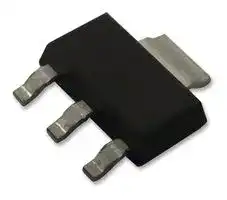


BSP030,115
Power MOSFET, N Channel, 30 V, 5 A, 0.02 ohm, SOT-223, Surface Mount
- Manufacturer: NEXPERIA
- Product type: Single MOSFETs
- No. of Pins: 4Pins
- Channel Type: N Channel
- Power Dissipation: 8.3W
- Transistor Mounting: Surface Mount
- Transistor Polarity: N Channel
- Power Dissipation Pd: 8.3W
- Rds(on) Test Voltage: 10V
- On Resistance Rds(on): 0.02ohm
- Transistor Case Style: SOT-223
- Drain Source Voltage Vds: 30V
- Operating Temperature Max: 150°C
- Continuous Drain Current Id: 5A
- Drain Source On State Resistance: 0.02ohm
- Gate Source Threshold Voltage Max: 2V
| Delivery and price | |
|---|---|
| Units per pack | 1000 |
| Price | 0.299 € |
| Current stock | 10+ |
| Lead time | 30 days |
## **BSP030**

**Rev. 04 — 26 July 2000**

## **1. Description**

TrenchMOS™[1] technology.

Product availability:

BSP030 in SOT223.

## **2. Features**

I TrenchMOS™ technology

- I Fast switching

- I Low on-state resistance

- I Logic level compatible

- I Surface mount package.

## **3. Applications**

I Motor and actuator driver

- I Battery management

- I High speed, low resistance switch.

## **4. Pinning information**

**Table 1:**

|**Pin**<br>**Description**<br>**Simplifed outline**<br>**Symbol**|**Pin**<br>**Description**<br>**Simplifed outline**<br>**Symbol**|**Pin**<br>**Description**<br>**Simplifed outline**<br>**Symbol**|**Pin**<br>**Description**<br>**Simplifed outline**<br>**Symbol**|**Pin**<br>**Description**<br>**Simplifed outline**<br>**Symbol**|**Pin**<br>**Description**<br>**Simplifed outline**<br>**Symbol**|**Pin**<br>**Description**<br>**Simplifed outline**<br>**Symbol**|
|---|---|---|---|---|---|---|
|1<br>gate (g)<br>2<br>drain (d)<br>3<br>source (s)<br>4<br>drain (d)||**SOT223**<br>**N-channel MOSFET**<br>**2**<br>**3**<br>03ab45<br>d<br>g<br>s<br>03ab30|||||
||**4**||||||
||||||||
||||||||
||||||||
||||||||
||||||||
||||||||
||**1**||||||


1. TrenchMOS is a trademark of Royal Philips Electronics.

**==> picture [229 x 70] intentionally omitted <==**

**BSP030**

**Philips Semiconductors**

## **5. Quick reference data**

## **Table 2: Quick reference data**

|**Symbol**<br>**Parameter**|**Conditions**<br>**Typ**<br>**Max**<br>**Unit**|
|---|---|
|VDS<br>drain-source voltage (DC)|Tj= 25 to 150°C<br>−<br>30<br>V|
|ID<br>drain current (DC)|Tsp= 25°C; VGS= 4.5 V<br>−<br>10<br>A|
|Ptot<br>total power dissipation|Tsp= 25°C<br>−<br>8.3<br>W|
|Tj<br>junction temperature|−<br>150<br>°C|
|RDSon<br>drain-source on-state resistance|VGS= 10 V; ID= 5 A<br>20<br>30<br>mΩ|
||VGS= 4.5 V; ID= 2.5 A<br>30<br>50<br>mΩ|


## **6. Limiting values**

## **Table 3: Limiting values**

In accordance with the Absolute Maximum Rating System (IEC 60134).

|**Symbol**<br>**Parameter**|**Conditions**<br>**Min**<br>**Max**<br>**Unit**|
|---|---|
|VDS<br>drain-source voltage (DC)|Tj= 25 to 150°C<br>−<br>30<br>V|
|VDGR<br>drain-gate voltage (DC)|Tj= 25 to 150°C; RGS= 20 kΩ<br>−<br>30<br>V|
|VGS<br>gate-source voltage (DC)|−<br>±20<br>V|
|ID<br>drain current (DC)|Tsp= 25°C; VGS= 4.5 V;<br>Figure 2and3<br>−<br>10<br>A|
||Tsp= 100°C; VGS= 4.5 V;Figure 2<br>−<br>6.3<br>A|
|IDM<br>peak drain current|Tsp= 25°C; pulsed; tp≤10µs;<br>Figure 3<br>−<br>40<br>A|
|Ptot<br>total power dissipation|Tsp= 25°C;Figure 1<br>−<br>8.3<br>W|
|Tstg<br>storage temperature|−65<br>+150<br>°C|
|Tj<br>operating junction temperature|−65<br>+150<br>°C|
|**Source-drain diode**||
|IS<br>source (diode forward) current (DC)|Tsp= 25°C<br>−<br>9<br>A|
|ISM<br>peak source (diode forward) current|Tsp= 25°C; pulsed; tp≤10µs<br>−<br>40<br>A|


© Philips Electronics N.V. 2000. All rights reserved.

9397 750 07268

**Rev. 04 — 26 July 2000**

**2 of 13**

**BSP030**

**Philips Semiconductors**

##

**==> picture [497 x 272] intentionally omitted <==**

**----- Start of picture text -----**<br>
03aa17 03aa25<br>120 120<br>Pder<br>Ider<br>(%)<br>100 (%)100<br>80 80<br>60 60<br>40 40<br>20 20<br>0 0<br>0 25 50 75 100 125 150 175 0 25 50 75 100 125 150 175<br>Tsp ( [o] C) Tsp ( [o] C)<br>Pder = ---------------------- PtotP ( tot25 ° C ) × 100 % V I der GS ≥ = 4.5 V----------------- I D ( I25D ° C - ) × 100 %<br>Fig 1. Normalized total power dissipation as a Fig 2. Normalized continuous drain current as a<br>function of solder point temperature. function of solder point temperature.<br>**----- End of picture text -----**<br>


**==> picture [292 x 159] intentionally omitted <==**

**----- Start of picture text -----**<br>
03ac23<br>10 [2]<br>(A)ID RDSon = VDS/ ID tp = 10 µs<br>10 100 µs<br>1 ms<br>P δ = tp D.C. 10 ms<br>1 T<br>100 ms<br>tp t<br>T<br>10 [-1]<br>10 [-1] 1 10 VDS (V) 10 [2]<br>**----- End of picture text -----**<br>


Tsp = 25 °C; IDM is single pulse.

**Fig 3. Safe operating area; continuous and peak drain currents as a function of drain-source voltage.**

© Philips Electronics N.V. 2000. All rights reserved.

9397 750 07268 **Product specification**

**Rev. 04 — 26 July 2000**

**3 of 13**

**BSP030**

**Philips Semiconductors**

## **7. Thermal characteristics**

## **Table 4: Thermal characteristics**

|**Symbol**|**Parameter**|**Conditions**|**Value**|**Unit**|
|---|---|---|---|---|
|Rth(j-sp)|thermal resistance from junction to solder|mounted on a metal clad substrate;|15|K/W|
||point|Figure 4|||
|Rth(j-a)|thermal resistance from junction to ambient|mounted on a printed circuit board;|100|K/W|
|||minimum footprint|||


## **7.1 Transient thermal impedance**

**==> picture [351 x 216] intentionally omitted <==**

**----- Start of picture text -----**<br>
03ac21<br>10 [2]<br>Zth(j-sp)<br>(K/W)<br>δ = 0.5<br>10<br>0.2<br>0.1<br>1 0.05<br>0.02 P δ = tp<br>T<br>10 [-1]<br>single pulse<br>tp t<br>T<br>10 [-2]<br>10 [-5] 10 [-4] 10 [-3] 10 [-2] 10 [-1] 1 10<br>tp (s)<br>Mounted on a metal clad substrate.<br>Fig 4. Transient thermal impedance from junction to solder point as a function of<br>pulse duration.<br>**----- End of picture text -----**<br>


© Philips Electronics N.V. 2000. All rights reserved.

9397 750 07268

**Rev. 04 — 26 July 2000**

**4 of 13**

**BSP030**

**Philips Semiconductors**

## **8. Characteristics**

**Table 5: Characteristics** Tj = 25 °C unless otherwise specified

|**Symbol**<br>**Parameter**|**Conditions**<br>**Min**<br>**Typ**<br>**Max**<br>**Unit**|
|---|---|
|**Static characteristics**||
|V(BR)DSS<br>drain-source breakdown<br>voltage|ID= 10µA; VGS= 0 V<br>Tj= 25°C<br>30<br>43<br>−<br>V|
||Tj=−55°C<br>27<br>−<br>−<br>V|
|VGS(th)<br>gate-source threshold voltage|ID= 1 mA; VDS= VGS;<br>Figure 9<br>Tj= 25°C<br>1<br>2<br>2.8<br>V|
||Tj= 150°C<br>0.6<br>−<br>−<br>V|
||Tj=−55°C<br>−<br>−<br>3.5<br>V|
|IDSS<br>drain-source leakage current|VDS= 24 V; VGS= 0 V<br>Tj= 25°C<br>−<br>10<br>100<br>nA|
||Tj= 150°C<br>−<br>−<br>10<br>µA|
|IGSS<br>gate-source leakage current|VGS=±20 V; VDS= 0 V<br>−<br>10<br>100<br>nA|
|RDSon<br>drain-source on-state<br>resistance|VGS= 10 V; ID= 5 A;<br>Figure 7and8<br>Tj= 25°C<br>−<br>20<br>30<br>mΩ|
||VGS= 5 V; ID= 2.5 A;<br>Figure 7and8<br>Tj= 25°C<br>−<br>30<br>50<br>mΩ|
||Tj= 150°C<br>−<br>−<br>85<br>mΩ|
|**Dynamic characteristics**||
|gfs<br>forward transconductance|VDS= 5 V; ID= 5.5 A;<br>Figure 11<br>−<br>12<br>−<br>S|
|Qg(tot)<br>total gate charge|ID= 5 A; VDS= 15 V;<br>VGS= 10 V;Figure 14<br>−<br>24<br>40<br>nC<br>−<br>3.3<br>−<br>nC<br>−<br>7.4<br>−<br>nC|
|Qgs<br>gate-source charge||
|Qgd<br>gate-drain (Miller) charge||
|Ciss<br>input capacitance|VGS= 0 V; VDS= 24 V;<br>f = 1 MHz;Figure 12<br>−<br>770<br>−<br>pF<br>−<br>265<br>−<br>pF<br>−<br>180<br>−<br>pF|
|Coss<br>output capacitance||
|Crss<br>reverse transfer capacitance||
|td(on)<br>turn-on delay time|VDD= 15 V; RD= 15Ω;<br>VGS= 10 V; RG= 6Ω<br>−<br>8<br>−<br>ns<br>−<br>10<br>−<br>ns<br>−<br>18<br>35<br>ns<br>−<br>24<br>−<br>ns<br>−<br>20<br>−<br>ns<br>−<br>44<br>150<br>ns|
|tr<br>turn-on rise time||
|ton<br>turn-on time||
|td(off)<br>turn-off delay time||
|tf<br>turn-off fall time||
|toff<br>turn-off time||


© Philips Electronics N.V. 2000. All rights reserved.

9397 750 07268

**Rev. 04 — 26 July 2000**

**5 of 13**

**BSP030**

**Philips Semiconductors**

**Table 5: Characteristics** …continued Tj = 25 °C unless otherwise specified

|**Symbol**|**Parameter**|**Conditions**|**Min**|**Typ**|**Max**|**Unit**|
|---|---|---|---|---|---|---|
|**Source-drain diode**|||||||
|VSD|source-drain (diode forward)|IS= 1.25 A; VGS= 0 V;|−|0.73|1.0|V|
||voltage|Figure 13|||||
|trr|reverse recovery time|IS= 1.25 A;|−|120|−|ns|
|Qr|recovered charge|dIS/dt =−100 A/µs;<br>VGS= 0 V; VDS= 25 V|−|150|−|nC|


**==> picture [157 x 168] intentionally omitted <==**

**----- Start of picture text -----**<br>
03ac25<br>20<br>ID 18 10 V VGS = 5 V Tj = 25 [o] C<br>(A)<br>16<br>14<br>12<br>3.4 V<br>10<br>8<br>3.2 V<br>6<br>3 V<br>4<br>2.8 V<br>2<br>2.6 V<br>0<br>0 0.2 0.4 0.6 0.8 1 1.2 1.4 1.6 1.8 2<br>VDS (V)<br>**----- End of picture text -----**<br>


**==> picture [161 x 166] intentionally omitted <==**

**----- Start of picture text -----**<br>
03ac27<br>20<br>ID<br>(A) 18 VDS > ID X RDSon<br>16<br>14<br>12<br>10 150 [o] C<br>8<br>6<br>4 Tj = 25 [o] C<br>2<br>0<br>0 0.5 1 1.5 2 2.5 3 3.5 4 4.5 5<br>VGS (V)<br>**----- End of picture text -----**<br>


**==> picture [36 x 10] intentionally omitted <==**

**----- Start of picture text -----**<br>
Tj = 25 °C<br>**----- End of picture text -----**<br>


**Fig 5. Output characteristics: drain current as a function of drain-source voltage; typical values.**

**==> picture [142 x 10] intentionally omitted <==**

**----- Start of picture text -----**<br>
Tj = 25 °C and 150 °C; VDS > ID × RDSon<br>**----- End of picture text -----**<br>


**Fig 6. Transfer characteristics: drain current as a function of gate-source voltage; typical values.**

**==> picture [189 x 193] intentionally omitted <==**

**----- Start of picture text -----**<br>
03ac26<br>0.2<br>RDSon 0.18 2.8V 3 V 3.2 V 3.4 V Tj = 25 [o] C<br>(Ω)<br>0.16<br>0.14<br>0.12<br>0.1<br>0.08<br>0.06<br>0.04 5V<br>0.02<br>VGS = 10V<br>0<br>0 2 4 6 8 10 12 14 16 18 20<br>ID (A)<br>Tj = 25 °C<br>**----- End of picture text -----**<br>


**Fig 7. Drain-source on-state resistance as a function of drain current; typical values.**

**==> picture [223 x 231] intentionally omitted <==**

**----- Start of picture text -----**<br>
03aa27<br>2.0<br>a<br>1.8<br>1.6<br>1.4<br>1.2<br>1.0<br>0.8<br>0.6<br>0.4<br>0.2<br>0<br>-60 -20 20 60 100 140 180<br>Tj ( [o] C)<br>a = -------------------------- RDSon -<br>RDSon ( 25 ° C )<br>Fig 8. Normalized drain-source on-state resistance<br>factor as a function of junction temperature.<br>**----- End of picture text -----**<br>


© Philips Electronics N.V. 2000. All rights reserved.

9397 750 07268

**Rev. 04 — 26 July 2000**

**6 of 13**

**BSP030**

**Philips Semiconductors**

**==> picture [174 x 166] intentionally omitted <==**

**----- Start of picture text -----**<br>
03aa34<br>3<br>VGS(th)<br>(V) 2.5<br>typ<br>2<br>1.5<br>min<br>1<br>0.5<br>0<br>-60 -20 20 60 100 140 180<br>Tj ( [[o]] C)<br>**----- End of picture text -----**<br>


**==> picture [497 x 397] intentionally omitted <==**

**----- Start of picture text -----**<br>
3 10 [-1] 03aa37<br>VGS(th) ID<br>(V) 2.5 (A)<br>10 [-2]<br>typ<br>2<br>min typ<br>10 [-3]<br>1.5<br>min 10 [-4]<br>1<br>10 [-5]<br>0.5<br>0 10 [-6]<br>-60 -20 20 60 100 140 180 0 0.5 1 1.5 2 2.5 3<br>Tj ( [[o]] C) VGS (V)<br>ID = 1 mA; VDS = VGS Tj = 25 °C; VDS = 5 V<br>Fig 9. Gate-source threshold voltage as a function of Fig 10. Sub-threshold drain current as a function of<br>junction temperature. gate-source voltage.<br>16 03ac28 03ac30<br>10 [4]<br>gfs(S) 14 Tj = 25 [o] C Ciss, Coss,<br>12 150 [o] C  Crss (pF)<br>10<br>8<br>10 [3]<br>6 Ciss<br>4<br>2 Coss<br>VDS > ID X RDSon<br>0 Crss<br>10 [2]<br>0 2 4 6 8 10 12 14 16 18 20<br>10 [-1] 1 10 10 [2]<br>ID (A) VDS (V)<br>**----- End of picture text -----**<br>


Tj = 25 °C and 150 °C; VDS > ID × RDSon

**Fig 11. Forward transconductance as a function of drain current; typical values.**

VGS = 0 V; f = 1 MHz

**Fig 12. Input, output and reverse transfer capacitances as a function of drain-source voltage; typical values.**

© Philips Electronics N.V. 2000. All rights reserved.

9397 750 07268

**Rev. 04 — 26 July 2000**

**7 of 13**

**BSP030**

**Philips Semiconductors**

##

**==> picture [411 x 170] intentionally omitted <==**

**----- Start of picture text -----**<br>
03ac29 03ac31<br>20 15<br>(A)IS 18 VGS = 0 V VGS(V) 1413 ID = 5 AVDS = 15 V<br>16 12<br>11 Tj = 25 [o] C<br>14<br>10<br>12 9<br>150 [o] C 8<br>10<br>7<br>8 Tj = 25 [o] C 6<br>5<br>6<br>4<br>4 3<br>2<br>2<br>1<br>0 0<br>0 0.2 0.4 0.6 0.8 1 1.2 0 5 10 15 20 25 30 35<br>VSD (V) QG (nC)<br>**----- End of picture text -----**<br>


**==> picture [117 x 10] intentionally omitted <==**

**----- Start of picture text -----**<br>
Tj = 25 °C and 150 °C; VGS = 0 V<br>**----- End of picture text -----**<br>


**==> picture [73 x 8] intentionally omitted <==**

**----- Start of picture text -----**<br>
ID = 5 A; VDS = 15 V<br>**----- End of picture text -----**<br>


**Fig 13. Source (diode forward) current as a function of Fig 14. Gate-source voltage as a function of gate source-drain (diode forward) voltage; typical charge; typical values. values.**

© Philips Electronics N.V. 2000. All rights reserved.

9397 750 07268

**Rev. 04 — 26 July 2000**

**8 of 13**

**BSP030**

**Philips Semiconductors**

## **9. Package outline**

**Plastic surface mounted package; collector pad for good heat transfer; 4 leads**

**==> picture [36 x 8] intentionally omitted <==**

**----- Start of picture text -----**<br>
SOT223<br>**----- End of picture text -----**<br>


**==> picture [482 x 574] intentionally omitted <==**

**----- Start of picture text -----**<br>
D B E A X<br>c<br>y<br>HE v M A<br>b1<br>4<br>Q<br>A<br>A1<br>1 2 3 Lp<br>e1 bp w M B detail X<br>e<br>0 2 4 mm<br>scale<br>DIMENSIONS (mm are the original dimensions)<br>UNIT A A1 bp b1 c D E e e1 HE Lp Q v w y<br>1.8 0.10 0.80 3.1 0.32 6.7 3.7 7.3 1.1 0.95<br>mm 4.6 2.3 0.2 0.1 0.1<br>1.5 0.01 0.60 2.9 0.22 6.3 3.3 6.7 0.7 0.85<br>OUTLINE  REFERENCES EUROPEAN<br>ISSUE DATE<br>VERSION  IEC  JEDEC  EIAJ PROJECTION<br>97-02-28<br> SOT223 SC-73<br>99-09-13<br>**----- End of picture text -----**<br>


## **Fig 15. SOT223.**

© Philips Electronics N.V. 2000. All rights reserved.

9397 750 07268

**Rev. 04 — 26 July 2000**

**9 of 13**

**BSP030**

**Philips Semiconductors**

## **10. Revision history**

## **Table 6: Revision history**

|**Rev**|**Date**|**CPCN**|**Description**|
|---|---|---|---|
|**04**|**20000726**|**HZG336**|**Product specifcation; fourth version; supersedes BSP030_3 of 970313.**|
||||Converted from VDMOS (Nijmegen) to TrenchMOS™ technology (Hazel Grove).|
|**03**|**19970313**|**-**|**Product specifcation; third version; supersedes BSP030_2 of 970120.**|
|**02**|**19970120**|**-**|**Product specifcation; second version; supersedes BSP030_1 of 961111.**|
|**01**|**19961111**|**-**|**Product specifcation; initial version.**|


© Philips Electronics N.V. 2000. All rights reserved.

9397 750 07268 **Product specification**

**Rev. 04 — 26 July 2000**

**10 of 13**

**BSP030**

**Philips Semiconductors**

## **11. Data sheet status**

|**Datasheet status**|**Product status**|**Defnition** [1]|
|---|---|---|
|Objective specifcation|Development|This data sheet contains the design target or goal specifcations for product development. Specifcation may|
|||change in any manner without notice.|
|Preliminary specifcation|Qualifcation|This data sheet contains preliminary data, and supplementary data will be published at a later date. Philips|
|||Semiconductors reserves the right to make changes at any time without notice in order to improve design and|
|||supply the best possible product.|
|Product specifcation|Production|This data sheet contains fnal specifcations. Philips Semiconductors reserves the right to make changes at any|
|||time without notice in order to improve design and supply the best possible product.|


[1] Please consult the most recently issued data sheet before initiating or completing a design.

## **12.**

## **13. Disclaimers**

The data in a short-form is extracted from a full data sheet with the same type number and title. For detailed information see the relevant data sheet or data handbook.

Limiting values given are in accordance with the Absolute Maximum Rating System (IEC 60134). Stress above one or more of the limiting values may cause permanent damage to the device. These are stress ratings only and operation of the device at these or at any other conditions above those given in the Characteristics sections of the specification is not implied. Exposure to limiting values for extended periods may affect device reliability.

**Application information  —** Applications that are described herein for any of these products are for illustrative purposes only. Philips Semiconductors make no representation or warranty that such applications will be suitable for the specified use without further testing or modification.

**Life support —** These products are not designed for use in life support appliances, devices, or systems where malfunction of these products can reasonably be expected to result in personal injury. Philips Semiconductors customers using or selling these products for use in such applications do so at their own risk and agree to fully indemnify Philips Semiconductors for any damages resulting from such application.

**Right to make changes —** Philips Semiconductors reserves the right to make changes, without notice, in the products, including circuits, standard cells, and/or software, described or contained herein in order to improve design and/or performance. Philips Semiconductors assumes no responsibility or liability for the use of any of these products, conveys no licence or title under any patent, copyright, or mask work right to these products, and makes no representations or warranties that these products are free from patent, copyright, or mask work right infringement, unless otherwise specified.

© Philips Electronics N.V. 2000 All rights reserved.

9397 750 07268

**Rev. 04 — 26 July 2000**

**11 of 13**

**BSP030**

**Philips Semiconductors**

## **Philips Semiconductors - a worldwide company**

**Argentina:** see South America **Australia:** Tel. +61 2 9704 8141, Fax. +61 2 9704 8139 **Austria:** Tel. +43 160 101, Fax. +43 160 101 1210 **Belarus:** Tel. +375 17 220 0733, Fax. +375 17 220 0773 **Belgium:** see The Netherlands **Brazil:** see South America **Bulgaria:** Tel. +359 268 9211, Fax. +359 268 9102 **Canada:** Tel. +1 800 234 7381 **China/Hong Kong:** Tel. +852 2 319 7888, Fax. +852 2 319 7700 **Colombia:** see South America **Czech Republic:** see Austria **Denmark:** Tel. +45 3 288 2636, Fax. +45 3 157 0044 **Finland:** Tel. +358 961 5800, Fax. +358 96 158 0920 **France:** Tel. +33 14 099 6161, Fax. +33 14 099 6427 **Germany:** Tel. +49 40 23 5360, Fax. +49 402 353 6300 **Hungary:** see Austria **India:** Tel. +91 22 493 8541, Fax. +91 22 493 8722 **Indonesia:** see Singapore **Ireland:** Tel. +353 17 64 0000, Fax. +353 17 64 0200 **Israel:** Tel. +972 36 45 0444, Fax. +972 36 49 1007 **Italy:** Tel. +39 039 203 6838, Fax +39 039 203 6800 **Japan:** Tel. +81 33 740 5130, Fax. +81 3 3740 5057 **Korea:** Tel. +82 27 09 1412, Fax. +82 27 09 1415 **Malaysia:** Tel. +60 37 50 5214, Fax. +60 37 57 4880 **Mexico:** Tel. +9-5 800 234 7381 **Middle East:** see Italy

**For all other countries apply to:** Philips Semiconductors, Marketing Communications, Building BE, P.O. Box 218, 5600 MD EINDHOVEN, The Netherlands, Fax. +31 40 272 4825

**Netherlands:** Tel. +31 40 278 2785, Fax. +31 40 278 8399 **New Zealand:** Tel. +64 98 49 4160, Fax. +64 98 49 7811 **Norway:** Tel. +47 22 74 8000, Fax. +47 22 74 8341 **Philippines:** Tel. +63 28 16 6380, Fax. +63 28 17 3474 **Poland:** Tel. +48 22 5710 000, Fax. +48 22 5710 001 **Portugal:** see Spain **Romania:** see Italy **Russia:** Tel. +7 095 755 6918, Fax. +7 095 755 6919 **Singapore:** Tel. +65 350 2538, Fax. +65 251 6500 **Slovakia:** see Austria **Slovenia:** see Italy **South Africa:** Tel. +27 11 471 5401, Fax. +27 11 471 5398 **South America:** Tel. +55 11 821 2333, Fax. +55 11 829 1849 **Spain:** Tel. +34 33 01 6312, Fax. +34 33 01 4107 **Sweden:** Tel. +46 86 32 2000, Fax. +46 86 32 2745 **Switzerland:** Tel. +41 14 88 2686, Fax. +41 14 81 7730 **Taiwan:** Tel. +886 22 134 2451, Fax. +886 22 134 2874 **Thailand:** Tel. +66 23 61 7910, Fax. +66 23 98 3447 **Turkey:** Tel. +90 216 522 1500, Fax. +90 216 522 1813 **Ukraine:** Tel. +380 44 264 2776, Fax. +380 44 268 0461 **United Kingdom:** Tel. +44 208 730 5000, Fax. +44 208 754 8421 **United States:** Tel. +1 800 234 7381 **Uruguay:** see South America **Vietnam:** see Singapore **Yugoslavia:** Tel. +381 11 3341 299, Fax. +381 11 3342 553

**Internet:** http://www.semiconductors.philips.com

(SCA70)

© Philips Electronics N.V. 2000. All rights reserved.

9397 750 07268

**Rev. 04 — 26 July 2000**

**12 of 13**

**BSP030**

**Philips Semiconductors**

## **Contents**

|**1**|**Description**. . . . . . . . . . . . . . . . . . . . . . . . . . . . . 1|
|---|---|
|**2**|**Features**. . . . . . . . . . . . . . . . . . . . . . . . . . . . . . . 1|
|**3**|**Applications**. . . . . . . . . . . . . . . . . . . . . . . . . . . . 1|
|**4**|**Pinning information**. . . . . . . . . . . . . . . . . . . . . . 1|
|**5**|**Quick reference data**. . . . . . . . . . . . . . . . . . . . . 2|
|**6**|**Limiting values**. . . . . . . . . . . . . . . . . . . . . . . . . . 2|
|**7**|**Thermal characteristics**. . . . . . . . . . . . . . . . . . . 4|
|7.1|Transient thermal impedance . . . . . . . . . . . . . . 4|
|**8**|**Characteristics**. . . . . . . . . . . . . . . . . . . . . . . . . . 5|
|**9**|**Package outline**. . . . . . . . . . . . . . . . . . . . . . . . . 9|
|**10**|**Revision history**. . . . . . . . . . . . . . . . . . . . . . . . 10|
|**11**|**Data sheet status**. . . . . . . . . . . . . . . . . . . . . . . 11|
|**12**|**Definitions**. . . . . . . . . . . . . . . . . . . . . . . . . . . . 11|
|**13**|**Disclaimers**. . . . . . . . . . . . . . . . . . . . . . . . . . . . 11|


## **© Philips Electronics N.V. 2000.**

## **Printed in The Netherlands**

All rights are reserved. Reproduction in whole or in part is prohibited without the prior written consent of the copyright owner.

The information presented in this document does not form part of any quotation or contract, is believed to be accurate and reliable and may be changed without notice. No liability will be accepted by the publisher for any consequence of its use. Publication thereof does not convey nor imply any license under patent- or other industrial or intellectual property rights.

**==> picture [229 x 117] intentionally omitted <==**

**Date of release: 26 July 2000**

**Document order number: 9397 750 07268**
Updated at February 9, 2023
Nexperia is a dedicated global leader in discretes, logic, and MOSFET devices. Built on over half a century of semiconductor expertise and operating independently since 2017, the company produces consistently reliable components at an exceptional volume of 85 billion units annually. With its own manufacturing facilities, Nexperia delivers industry-leading small packages that combine power and thermal efficiency with best-in-class quality, meeting the rigorous standards of the automotive sector. Our extensive Nexperia portfolio is heavily focused on discrete semiconductors, providing engineers with a robust selection of core building blocks. This includes a comprehensive range of diodes and rectifiers, featuring a vast selection of Zener single diodes and Schottky diodes designed for precise voltage regulation and efficient power routing. Additionally, we offer an expansive array of bipolar transistors and single MOSFETs tailored for reliable switching and amplification in demanding applications. Beyond these primary offerings, the lineup extends into specialized circuit protection and passive components. This includes transient voltage suppressor (TVS) diodes, Zener array diodes, and small signal diodes, alongside dual MOSFETs and fast recovery rectifiers. For comprehensive design needs, the selection also encompasses integrated passive filters, common mode chokes, and precision timers and oscillators, ensuring a complete solution for high-performance electronic systems.
About Novapart
Novapart is a B2B electronic component broker specialising in stock shortages and cost reduction. We source hard-to-find parts and identify compliant alternatives across a catalogue of 410,000+ components from 500+ manufacturers.
Learn more →Stock Shortage Specialist
When a component is unavailable, discontinued or has an unacceptable lead time, we tap into our network of vetted European and Asian distributors to source what you need — without compromising on quality or traceability.
Request a quote →Compliant Alternatives
We identify pin-to-pin, electrically equivalent substitutes that meet the same certifications (RoHS, AEC-Q100, REACH) as your original specification — validated against datasheets, not just part numbers. Often at a lower cost.
BOM Analysis service →