


BSG0811NDATMA1
Dual MOSFET, N Channel, 25 V, 25 V, 50 A, 50 A, 2400 µohm
- Manufacturer: INFINEON
- Product type: Dual MOSFETs
- Transistor Polarity:Dual N Channel; Continuous Drain Current Id:50A; Drain Source Voltage Vds:25V; On Resistance Rds(on):0.0024ohm; Rds(on) Test Voltage Vgs:10V; Threshold Voltage Vgs:
- MSL: MSL 1 - Unlimited
- SVHC: No SVHC (25-Jun-2025)
- No. of Pins: 8Pins
- Channel Type: N Channel
- Product Range: OptiMOS 5 Series
- Qualification: -
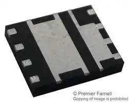
- Transistor Case Style: TISON
- Operating Temperature Max: 150°C
- Power Dissipation N Channel: 6.25W
- Power Dissipation P Channel: 6.25W
- Drain Source Voltage Vds N Channel: 25V
- Drain Source Voltage Vds P Channel: 25V
- Continuous Drain Current Id N Channel: 50A
- Continuous Drain Current Id P Channel: 50A
- Drain Source On State Resistance N Channel: 2400µohm
- Drain Source On State Resistance P Channel: 2400µohm
| Delivery and price | |
|---|---|
| Units per pack | 5000 |
| Price | 0.744 € |
| Current stock | 1000+ |
| Lead time | 30 days |
## **BSG0811ND**

## **Product Summary**

## **Power Block**

**==> picture [473 x 187] intentionally omitted <==**

**----- Start of picture text -----**<br>
|||||||||
|---|---|---|---|---|---|---|---|
|Q1|Q2|
|Features|
|• Dual asymmetric N-channel OptiMOS™5 MOSFET|V|DS|25|25|V|
|• Logic level (4.5V rated)|R|DS(on),max|V|GS=10 V|3|0.8|mW|
|• Optimized for high performance buck converters|V|GS=4.5 V|4|1.1|
|• Qualified according to JEDEC|[1)]|for target applications|I|D|50|50|A|
|• Pb-free lead  plating; RoHS compliant|S1/D2  (VPhase)|(5)|Q1|(9)|(4)|D1  (Vin)|
|S1/D2  (VPhase)|a|(6)|l|(3)|D1  (Vin)|
|• Halogen-free according to IEC61249-2-21|S1/D2  (VPhase)|(7)|(2)|S1  (VPhase)|
|sp|Q2|i|t|ae|
|G2  (GLS)|F@|GP|(8)|lL|7|(1)|G1  (GHS)|
|(10)|S2  (GND)|
|Top view|

**----- End of picture text -----**<br>


- Dual asymmetric N-channel OptiMOS™5 MOSFET

**==> picture [232 x 30] intentionally omitted <==**

**----- Start of picture text -----**<br>
||||
|---|---|---|
|Type|Package|Marking|
|BSG0811ND|PG-TISON8-4|0811ND|

**----- End of picture text -----**<br>


**Maximum ratings,** at _T_ j=25 °C, unless otherwise specified[2)]

**==> picture [464 x 313] intentionally omitted <==**

**----- Start of picture text -----**<br>
|||||||||||
|---|---|---|---|---|---|---|---|---|---|
|Parameter|Symbol|Conditions|Value|Unit|
|Q1|Q2|
|Continuous drain current|I|D|T|C=70 °C,|V|GS=10 V|50|50|A|
|T|C=70 °C,|V|GS=4.5 V|50|50|
|T|A=25 °C,|
|31|50|
|V|GS=4.5 V|[3)]|
|T|A=25 °C,|
|19|41|
|V|GS=4.5 V|[4)]|
|Pulsed drain current|I|D,pulse|T|C=70 °C|160|160|
|Q1:|I|D=10 A,|
|Avalanche energy, single pulse|E|AS|Q2:|I|D=20 A,|30|160|mJ|
|R|GS=25 W|
|Gate source voltage|V|GS|±16|V|
|Power dissipation|P|tot|T|A=25 °C|[3)]|6.25|6.25|W|
|T|A=25 °C|[4)]|2.5|2.5|
|Operating and storage temperature|T|j,|T|stg|-55 ... 150|°C|
|IEC climatic category; DIN IEC 68-1|55/150/56|

**----- End of picture text -----**<br>


1) J-STD20 and JESD22

Rev.2.2

page 1

2017-08-11

|**BSG0811ND**<br>**Parameter**<br>**Symbol Conditions**<br>**Unit**<br>**min.**<br>**typ.**<br>**max.**<br>**Values**<br>Cinfineon~~rer~~|**BSG0811ND**<br>**Parameter**<br>**Symbol Conditions**<br>**Unit**<br>**min.**<br>**typ.**<br>**max.**<br>**Values**<br>Cinfineon~~rer~~|**BSG0811ND**<br>**Parameter**<br>**Symbol Conditions**<br>**Unit**<br>**min.**<br>**typ.**<br>**max.**<br>**Values**<br>Cinfineon~~rer~~|**BSG0811ND**<br>**Parameter**<br>**Symbol Conditions**<br>**Unit**<br>**min.**<br>**typ.**<br>**max.**<br>**Values**<br>Cinfineon~~rer~~|**BSG0811ND**<br>**Parameter**<br>**Symbol Conditions**<br>**Unit**<br>**min.**<br>**typ.**<br>**max.**<br>**Values**<br>Cinfineon~~rer~~|**BSG0811ND**<br>**Parameter**<br>**Symbol Conditions**<br>**Unit**<br>**min.**<br>**typ.**<br>**max.**<br>**Values**<br>Cinfineon~~rer~~|**BSG0811ND**<br>**Parameter**<br>**Symbol Conditions**<br>**Unit**<br>**min.**<br>**typ.**<br>**max.**<br>**Values**<br>Cinfineon~~rer~~|**BSG0811ND**<br>**Parameter**<br>**Symbol Conditions**<br>**Unit**<br>**min.**<br>**typ.**<br>**max.**<br>**Values**<br>Cinfineon~~rer~~|
|---|---|---|---|---|---|---|---|
|**Thermal characteristics**||||||||
|Thermal resistance, junction -|Q1|_R_thJC||-|-|4.3|K/W|
|case|Q2|||-|-|1.8||
|Thermal resistance, junction -<br>ambient2)|Q1 <br>Q2|_R_thJA|application specific<br>board3)|-|-|20||
||Q1<br>Q2||6 cm2cooling area4)|-|-|50||


**Electrical characteristics,** at _T_ j=25 °C, unless otherwise specified

## **Static characteristics**

Drain-source breakdown voltage Q1 _V_ (BR)DSS _V_ GS=0 V, _I_ D=1 mA 25[6)] - - V Q2 ~~TT~~ Gate threshold voltage Q1 _V_ GS(th) _V_ DS= _V_ GS, _I_ D=250 µA 1.2 1.6 2 Q2 ~~Te~~ Zero gate voltage drain current Q1 _I_ DSS _V_ DS=25 V, _V_ GS=0 V, - - 1 µA _T_ =25 °C Q2 j ~~eee~~ Q1 _V_ DS=25 V, _V_ GS=0 V, - - 100 _T_ =150 °C Q2 j ~~A~~ Gate-source leakage current Q1 _I_ GSS _V_ GS=20 V, _V_ DS=0 V - - 100 nA Q2 ~~cee~~ Drain-source on-state Q1 _R_ DS(on) - 3.2 4.0 mW _V_ GS=4.5 V, _I_ D=20 A ~~||~~ resistance Q2 - 0.9 1.1 ~~oe~~ Q1 - 2.4 3.0 _V_ GS=10 V, _I_ D=20 A Q2 - 0.7 0.8 ~~a: =—===~~ Gate resistance Q1 _R_ G - 0.7 1.2 W Q2 - 0.7 1.2 ~~eee=~~ Transconductance Q1 _g_ fs | _V_ DS|>2| _I_ D| _R_ DS(on)max, 46 93 ~~.~~ - S Q2 _I_ D=20 A 90 180 - ~~**=** ==~~

- 2) Only one of both transistors active

- 3) 8 Layers copper 70µm thickness. PCB in still air.

4) Device on 40 mm x 40 mm x 1.5 mm epoxy PCB FR4 with 6 cm2 (one layer, 70 µm thick) copper area for drain connection. PCB is vertical in still air.

Rev.2.2

page 2

2017-08-11

**BSG0811ND**

|**Parameter**||**Symbol **|**Conditions**<br>**Values**|**Unit**|
|---|---|---|---|---|
||||**min.**<br>**typ.**<br>**max.**||
|**Dynamic characteristics**|||||
|Input capacitance<br>Output capacitance<br>Reverse transfer capacitance<br>Turn-on delay time<br>Rise time<br>Turn-off delay time<br>Fall time|Q1 _C_iss<br>Q2<br>Q1 _C_oss<br>Q2<br>Q1 Crss<br>Q2<br>Q1 _t_d(on)<br>Q2<br>Q1 _t_r<br>Q2<br>Q1 _t_d(off)<br>Q2<br>Q1 _t_f<br>Q2<br>~~Sy~~<br>~~|~~<br>~~Sy~~<br>~~|~~<br>~~Sy~~<br>~~|~~<br>~~Sy~~<br>~~|~~<br>~~4~~<br>~~|~~<br>~~4~~<br>~~|~~<br>~~4~~<br>~~|~~||-<br>780<br>1100<br>-<br>2700<br>3700<br>-<br>390<br>520<br>-<br>1400<br>1900<br>-<br>38<br>-<br>-<br>130<br>-<br>-<br>4.3<br>-<br>5.6<br>-<br>-<br>4.7<br>-<br>-<br>4.3<br>-<br>-<br>4.3<br>-<br>-<br>8.8<br>-<br>-<br>1.4<br>-<br>-<br>2.6<br>-<br>_V_GS=0 V,<br>_V_DS= 12 V,_f_=1 MHz<br>_V_IN=12 V,<br>_V_DRV=5 V,<br>_F_SW=500 KHz,<br>_I_OUT=30 A5)<br>~~**F**t~~<br>~~t~~<br>~~**F**t~~<br>~~t~~<br>~~Ft~~<br>~~PFtT~~<br>~~PF tT~~<br>~~PFtT~~<br>~~**F**t~~<br>~~t~~<br>~~**F**t~~<br>~~t~~<br>~~**F**t~~<br>~~t~~|pF<br>ns|
|**Gate Charge Characteristics**|||||
|Gate to source charge<br>Gate to drain charge|Q1 _Q_gs<br>_Q_gd<br>~~S|~~<br>~~|~~||-<br>2.0<br>-<br>-<br>1.4<br>-<br>~~Ft~~<br>~~Pt~~|nC|
|Gate charge total||_Q_g<br>~~|~~|-<br>5.6<br>8.4<br>~~Ft~~||
|Gate plateau voltage<br>Gate to source charge|Q2|_V_plateau<br> _Q_gs<br>~~|~~<br>~~|~~|-<br>2.6<br>-<br>-<br>6.4<br>-<br>_V_DD=12 V,<br>_I_D=30 A,<br>_V_GS=0 to 4.5 V<br>~~Pt~~<br>~~Ft~~|V<br>nC|
|Gate to drain charge||_Q_gd<br>~~|~~|-<br>4.7<br>-<br>~~Pt~~||
|Gate charge total||_Q_g<br>~~|~~|-<br>20<br>29<br>~~Ft~~||
|Gate plateau voltage<br>Output charge<br>5)For more information see application note n° TBD|_V_plateau<br>-<br>2.3<br>-<br>Q1 _Q_oss<br>-<br>8<br>-<br>Q2<br>-<br>27<br>-<br>For more information see application note n° TBD<br>_V_DD=12 V,_V_GS=0 V<br>~~}-—E~~<br>~~ee~~|||V<br>nC|


- 5)  For more information see application note n° TBD

6)  The device can withstand a pulse of not more than 30 V for a duration of up to 2 ns at a frequency of 600 kHz with maximum buck converter input voltage _V_ IN=16 V.

Rev.2.2

page 3

2017-08-11

## **BSG0811ND**

|**Parameter**||**Symbol **|**Conditions**||**Values**||**Unit**|
|---|---|---|---|---|---|---|---|
|||||**min.**|**typ.**|**max.**||
|**Reverse Diode**||||||||
|Diode continuous forward current<br>Q1 _I_S<br>Q2<br>Diode pulse current<br>Q1 _I_S,pulse<br>Q2<br>Diode forward voltage<br>Q1 _V_SD<br>Q2<br>Reverse recovery charge<br>Q1 _Q_rr<br>Q2<br>_T_C=25 °C<br>_V_GS=0 V,_I_F=20 A,<br>_T_j=25 °C<br>_V_R=12 V,_I_F=_I_S,<br>d_i_F/d_t_=100 A/µs<br>~~I~~||||-<br>-<br>-<br>-<br>-<br>-<br>-<br>-|-<br>-<br>-<br>-<br>0.84<br>0.77<br>10<br>20|29<br>50<br>160<br>160<br>1<br>1<br>-<br>-|A<br>V<br>nC|


Rev.2.2

page 4

2017-08-11

**BSG0811ND**

## **1 Power dissipation (Q1) 2 Power dissipation (Q2)**

_P_ tot=f( _T_ A)[4)]

_P_ tot=f( _T_ A)[4)]

**==> picture [466 x 610] intentionally omitted <==**

**----- Start of picture text -----**<br>
3 3<br>2.5 2.5<br>2 2<br>1.5 1.5<br>1 1<br>0.5 0.5<br>0 0<br>0 40 80 120 160 0 40 80 120 160<br>T A [°C]  T A [°C]<br>3 Drain current (Q1) 4 Drain current (Q2)<br>=f( T  C)) I  D=f( T  C)<br>parameter:  V  GS≥10 V≥10 V parameter:  V  GS≥10 V<br>60 60<br>50 50<br>40 40<br>30 30<br>20 20<br>10 10<br>0 0<br>0 40 80 120 160 0 40 80 120 160<br>T C [°C]  T C [°C]<br> [W]   [W]<br>tot tot<br>P P<br> [A]   [A]<br>I D I D<br>**----- End of picture text -----**<br>


## **3 Drain current (Q1)**

_I_ D=f( _T_ C))

parameter: _V_ GS≥10 V≥10 V

Rev.2.2

page 5

2017-08-11

**BSG0811ND**

## **5 Safe operating area (Q1)**

_I_ D=f( _V_ DS); _T_ C=25 °C; _D_ =0 parameter: _t_ p

## **6 Safe operating area (Q2)**

_I_ D=f( _V_ DS); _T_ C=25 °C; _D_ =0

parameter: _t_ p

**==> picture [460 x 607] intentionally omitted <==**

**----- Start of picture text -----**<br>
10 [3 ] 10 [3 ]<br>1 µs  1 µs<br>10 [2 ] 10 µs  10 [2 ] 10 µs<br>100 µs  100 µs<br>1 ms<br>“|<br>1 ms  10 ms<br>10 [1 ] 10 [1 ]<br>10 ms  \<br>DC<br>DC<br>10 [0 ] 10 [0 ]<br>10 [-1 ] 10 [-1 ]<br>10 [-1 ] 10 [0 ] 10 [1 ] 10 [2 ] 10 [-1 ] 10 [0 ] 10 [1 ] 10<br>V DS [V]  V DS [V]<br>7 Max. transient thermal impedance (Q1) 8 Max. transient thermal impedance (Q2)<br> thJC=f(=f( t  p)) Z  thJC=f( t  p)<br>parameter:  D  = t  p// T parameter:  D  = t  p/ T<br>10 [1 ] 10 [1 ]<br>0.5  10 [0 ] 0.5<br>0.2  0.2<br>10 [0 ]<br>0.1<br>0.1<br>0.05<br>0.05  0.02<br>10 [-1 ] 0.01<br>0.02<br>single pulse<br>0.01<br>single pulse<br>10 [-1 ] 10 [-2 ]<br>10 [-5 ] 10 [-4 ] 10 [-3 ] 10 [-2 ] 10 [-1 ] 10 [0 ] 10 [-5 ] 10 [-4 ] 10 [-3 ] 10 [-2 ] 10 [-1 ] 10<br>t p [s]  t p [s]<br>[A]   [A]<br>I D I D<br> [K/W]   [K/W]<br>thJC thJC<br>Z Z<br>**----- End of picture text -----**<br>


**7 Max. transient thermal impedance (Q1)** _Z_ thJC=f(=f( _t_ p))

parameter: _D_ = _t_ p// _T_

Rev.2.2

page 6

2017-08-11

**BSG0811ND**

## **9 Typ. output characteristics (Q1)**

_I_ D=f( _V_ DS); _T_ j=25 °C

parameter: _V_ GS

## **10 Typ. output characteristics (Q2)**

_I_ D=f( _V_ DS); _T_ j=25 °C

parameter: _V_ GS

**==> picture [462 x 267] intentionally omitted <==**

**----- Start of picture text -----**<br>
160 4 V  400<br>4.5 V<br>10 V  10 V<br>4 V<br>3.5 V  3.3 V<br>4.5 V<br>3.5 V<br>120 300<br>3.3 V<br>3 V<br>3 V<br>2.8 V<br>80 200<br>2.8 V<br>40 100<br>0 0<br>0 1 2 3 0 1 2 3<br>V DS [V]  V DS [V]<br> [A]   [A]<br>I D I D<br>**----- End of picture text -----**<br>


## **11 Typ. drain-source on resistance (Q1)**

_R_ DS(on)=f( _I_ D); _T_ j=25 °C parameter: _V_ GS

## **12 Typ. drain-source on resistance (Q2)**

_R_ DS(on)=f( _I_ D); _T_ j=25 °C

parameter: _V_ GS

**==> picture [463 x 267] intentionally omitted <==**

**----- Start of picture text -----**<br>
10 2<br>8 3 V<br>1.5<br>3.3 V<br>6 3.5 V<br>3 V<br>1 4 V<br>3.3 V<br>4.5 V<br>4 3.5 V  5 V<br>4 V<br>10 V<br>4.5 V<br>5 V<br>10 V  0.5<br>2<br>0 0<br>0 20 40 60 80 0 20 40 60 80<br>I D [A]  I D [A]<br>]  ]<br>W W<br> [m  [m<br>DS(on) DS(on)<br>R R<br>**----- End of picture text -----**<br>


Rev.2.2

page 7

2017-08-11

**BSG0811ND**

## **13 Typ. transfer characteristics (Q1)**

_I_ D=f( _V_ GS); | _V_ DS |>2 | _I_ D| _R_ DS(on)max parameter: _T_ j

## **14 Typ. transfer characteristics (Q2)**

_I_ D=f( _V_ GS); _|V_ DS |>2 | _I_ D _| R_ DS(on)max parameter: _T_ j

**==> picture [466 x 611] intentionally omitted <==**

**----- Start of picture text -----**<br>
160 400<br>120 | 300 |<br>80 200<br>150 °C<br>40 100<br>25 °C<br>150 °C<br>25 °C<br>i t d<br>0 0<br>0 1 2 3 4 0 1 2 3 4<br>V GS [V]  V GS [V]<br>15 Drain-source on-state resistance (Q1) 16 Drain-source on-state resistance (Q2)<br> DS(on)=f(=f( T  j); );  I  D=20 A; =20 A;  V  GS=10 V=10 V R  DS(on)=f( T  j);  I  D=20 A;  V  GS=10 V<br>7 2<br>6<br>1.5<br>5<br>4<br>1<br>3 typ<br>typ<br>2<br>0.5<br>1<br>0 0<br>-60 -20 20 60 100 140 180 -60 -20 20 60 100 140 180<br>T j [°C]  T j [°C]<br> [A]   [A]<br>I D I D<br>]  ]<br>W W<br>[m  [m<br>DS(on) DS(on)<br>R R<br>**----- End of picture text -----**<br>


## **15 Drain-source on-state resistance (Q1)**

_R_ DS(on)=f(=f( _T_ j); ); _I_ D=20 A; =20 A; _V_ GS=10 V=10 V

Rev.2.2

page 8

2017-08-11

**BSG0811ND**

## **17 Typ. gate threshold voltage (Q1)**

_V_ GS(th)=f( _T_ j); _V_ GS= _V_ DS; _I_ D=250 µA

## **18 Typ. gate threshold voltage (Q2)**

_V_ GS(th)=f( _T_ j); _V_ GS= _V_ DS; _I_ D=250 µA

**==> picture [473 x 610] intentionally omitted <==**

**----- Start of picture text -----**<br>
2.8 2.8<br>2.4 2.4<br>2 2<br>1.6 1.6<br>1.2 1.2<br>0.8 0.8<br>0.4 0.4<br>0 0<br>-60 -20 20 60 100 140 180 -60 -20 20 60 100 140 180<br>T j [°C]  T j [°C]<br>19 Typ. capacitances (Q1) 20 Typ. capacitances (Q2)<br>C  =f( V  DS);  V  GS=0 V;  f  =1 MHz C  =f( V  DS);  V  GS=0 V;  f  =1 MHz<br>10 [4] 10 [4 ]<br>Ciss  Ciss<br>10 [3 ] = g l<br>10 [3 ]<br>Coss<br>Coss<br>10 [2 ]<br>Crss<br>Crss<br>‘ t a m cue<br>10 [2 ]<br>10 [1 ]<br>10 [0 ] 10 [1 ]<br>0 5 10 15 20 25 0 5 10 15 20 25<br>V DS [V]  V DS [V]<br> [V]   [V]<br>GS(th) GS(th)<br>V V<br> [pF]   [pF]<br>C C<br>**----- End of picture text -----**<br>


Rev.2.2

page 9

2017-08-11

**BSG0811ND**

## **21 Forward characteristics of reverse diode (Q1)**

**==> picture [468 x 705] intentionally omitted <==**

**----- Start of picture text -----**<br>
21 Forward characteristics of reverse diode (Q1) 22 Forward characteristics of reverse diode (Q2)<br>I  F=f( V  SD) I  F=f( V  SD)<br>parameter:  T  j parameter:  T  j<br>10 [3 ] 10 [3 ]<br>10 [2 ] 10 [2 ]<br>25 °C<br>150 °C  25 °C  150 °C<br>10 [1 ] 10 [1 ]<br>10 [0 ] 10 [0 ]<br>10 [-1 ] 10 [-1 ]<br>10 [-2 ] ae 10 [-2 ] ge<br>0 0.4 0.8 1.2 0 0.4 0.8 1.2<br>V SD [V]  V SD [V]<br>23 Avalanche characteristics (Q1) 24 Avalanche characteristics (Q2)<br>I  AS=f( t  AV);  R  GS=25 W I  AS=f( t  AV);  R  GS=25 W<br>parameter:  T  j(start) parameter:  T  j(start)<br>10 [2 ] 10 [2 ]<br>25 °C<br>125 °C<br>100 °C<br>10 [1 ] 25 °C  10 [1 ]<br>100 °C<br>125 °C<br>10 [0 ] SS 10 [0 ]<br>10 [0 ] 10 [1 ] 10 [2 ] 10 [3 ] 10 [0 ] 10 [1 ] 10 [2 ] 10 [3 ]<br>t AV [µs]  t AV [µs]<br>Rev.2.2 page 10<br> [A]   [A]<br>I F I F<br> [A]   [A]<br>I AV I AV<br>**----- End of picture text -----**<br>


Rev.2.2

2017-08-11

**BSG0811ND**

## **25 Typ. gate charge (Q1)**

_V_ GS=f( _Q_ gate); _I_ D=20 A pulsed parameter: _V_ DD

## **26 Typ. gate charge (Q2)**

_V_ GS=f( _Q_ gate); _I_ D=20 A pulsed parameter: _V_ DD

**==> picture [464 x 268] intentionally omitted <==**

**----- Start of picture text -----**<br>
10 10<br>8 8<br>12 V  20 V<br>5 V<br>12 V<br>6 20 V  6<br>5 V<br>4 / 4 VA<br>2 2<br>[- [<br>0 0<br>0 2 4 6 8 10 12 14 0 10 20 30 40 50<br>Q gate [nC]  Q gate [nC]<br> [V]   [V]<br>GS GS<br>V V<br>**----- End of picture text -----**<br>


## **27 Drain-source breakdown voltage (Q1)**

_V_ BR(DSS)=f( _T_ j); _I_ D=1 mA

## **28 Drain-source breakdown voltage (Q2)**

_V_ BR(DSS)=f( _T_ j); _I_ D=1 mA

**==> picture [466 x 268] intentionally omitted <==**

**----- Start of picture text -----**<br>
28 28<br>27 27<br>26 26<br>25 25<br>24 24<br>23 23<br>22 22<br>21 21<br>20 20<br>-60 -20 20 60 100 140 180 -60 -20 20 60 100 140 180<br>T j [°C]  T j [°C]<br> [V]   [V]<br>BR(DSS) BR(DSS)<br>V V<br>**----- End of picture text -----**<br>


Rev.2.2

page 11

2017-08-11

**BSG0811ND**

## **Package Outline PG-TISON8-4**

Rev.2.2

page 12

2017-08-11

**BSG0811ND**

## **Boardpads & Apertures**

## **PG-TISON8-4**

**All the dimensions in mm**

Rev.2.2

page 13

2017-08-11

**BSG0811ND**

## BSG0811ND

|Previous Revision|Previous Revision||
|---|---|---|
|Revision|Date|Subjects (major changes since last revision)|
|2.0|2015-03-17|Release of final version|
|2.1|2016-03-24|Update package drawing|
|2.2|2017-08-25|Update package outline|


## **erratum@infineon.com**

## **Information**

**www.infineon.com** ).

## **Warnings**

14
Updated at June 9, 2026
Infineon Technologies is a globally recognized leader in semiconductor solutions, renowned for driving innovation in power management, energy efficiency, and modern mobility. With a strong legacy of engineering excellence, the company provides highly reliable components designed to meet the rigorous demands of industrial, automotive, and advanced commercial applications. The core of our Infineon portfolio is centered on their industry-leading discrete semiconductors. We offer an extensive selection of single and dual MOSFETs, alongside a robust range of single IGBTs and advanced IGBT modules. These flagship power transistors are essential for high-efficiency power conversion and motor control, providing engineers with superior thermal performance and minimized switching losses. Beyond advanced field-effect transistors, the selection includes a comprehensive array of diodes and rectifiers, heavily featuring Schottky diodes, as well as fast-recovery and RF/PIN diodes. This power foundation is further supported by bipolar transistors, intelligent power modules, and thyristor SCR modules, delivering the critical building blocks required for complex power system designs. To support broader system integration, the portfolio also encompasses specialized solutions such as solid-state relays, AC/DC LED driver ICs, and Bluetooth communications modules. From high-power industrial rectifiers to wireless connectivity adapters, Infineon equips designers with the precision components needed to build efficient, scalable, and fully connected electronic systems.
About Novapart
Novapart is a B2B electronic component broker specialising in stock shortages and cost reduction. We source hard-to-find parts and identify compliant alternatives across a catalogue of 410,000+ components from 500+ manufacturers.
Learn more →Stock Shortage Specialist
When a component is unavailable, discontinued or has an unacceptable lead time, we tap into our network of vetted European and Asian distributors to source what you need — without compromising on quality or traceability.
Request a quote →Compliant Alternatives
We identify pin-to-pin, electrically equivalent substitutes that meet the same certifications (RoHS, AEC-Q100, REACH) as your original specification — validated against datasheets, not just part numbers. Often at a lower cost.
BOM Analysis service →