
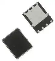


BSC014N04LSATMA1
Power MOSFET, N Channel, 40 V, 100 A, 1400 µohm, TDSON, Surface Mount
- Manufacturer: INFINEON
- Product type: Single MOSFETs
- Transistor Polarity:N Channel; Continuous Drain Current Id:100A; Drain Source Voltage Vds:40V; On Resistance Rds(on):0.0011ohm; Rds(on) Test Voltage Vgs:10V; Threshold Voltage Vgs:2V; Po
- MSL: MSL 1 - Unlimited
- SVHC: No SVHC (25-Jun-2025)
- No. of Pins: 8Pins
- Channel Type: N Channel
- Product Range: -
- Qualification: -
- Power Dissipation: 2.5W
- Transistor Mounting: Surface Mount
- Rds(on) Test Voltage: 10V
- Transistor Case Style: TDSON
- Drain Source Voltage Vds: 40V
- Operating Temperature Max: 150°C
- Continuous Drain Current Id: 100A
- Drain Source On State Resistance: 1400µohm
- Gate Source Threshold Voltage Max: 2V
| Delivery and price | |
|---|---|
| Units per pack | 3000 |
| Price | 0.526 € |
| Current stock | 1000+ |
| Lead time | 30 days |
**BSC014N04LS**
## **MOSFET OptiMOS[TM]**
## **Features**
* Optimized for synchronous rectification
_R_ DS(on)
1)
|**Parameter**<br>~~1~~<br>~~Key Performance~~|**Value**<br>~~Performance Parameters~~|**Unit**<br>~~Parameters~~|
|---|---|---|
|_V_DS|40|V|
|_R_DS(on),max|1.4|mΩ|
|_I_D|100|A|
|_Q_oss|54|nC|
|_Q_g(0V..10V)|61|nC|
**==> picture [143 x 204] intentionally omitted <==**
**----- Start of picture text -----**<br>
8<br>7<br>6<br>5<br>GES<br>“Agee,<br>1 = 5<br>2 6<br>3 4 acS 7 8<br>4<br>3<br>2<br>1<br>S 1 L a 8 D<br>S 2 | | 7 D<br>S 3 6 D<br>H IKED a<br>G 4 5 D<br>**----- End of picture text -----**<br>
|~~Type/OrderingCode|~~|**Package**<br>~~|~~<br>~~|~~|**Marking**|~~RelatedLinks~~|
|---|---|---|---|
|BSC014N04LS<br>~~Type/OrderingCode |~~|TDSON-8 FL<br>~~|~~<br>~~|~~|014N04LS|-<br>~~Related Links~~|
1) J-STD20 and JESD22
Final Data Sheet
1
**OptiMOS[TM] �Power-MOSFET,�40�V BSC014N04LS**
**==> picture [120 x 53] intentionally omitted <==**
## **Table�of�Contents**
Description . . . . . . . . . . . . . . . . . . . . . . . . . . . . . . . . . . . . . . . . . . . . . . . . . . . . . . . . . . . . . . . . . . . . . . . . . . . . . 1 Maximum ratings . . . . . . . . . . . . . . . . . . . . . . . . . . . . . . . . . . . . . . . . . . . . . . . . . . . . . . . . . . . . . . . . . . . . . . . . 3 Thermal characteristics . . . . . . . . . . . . . . . . . . . . . . . . . . . . . . . . . . . . . . . . . . . . . . . . . . . . . . . . . . . . . . . . . . . . 3 Electrical characteristics . . . . . . . . . . . . . . . . . . . . . . . . . . . . . . . . . . . . . . . . . . . . . . . . . . . . . . . . . . . . . . . . . . . 4 Electrical characteristics diagrams . . . . . . . . . . . . . . . . . . . . . . . . . . . . . . . . . . . . . . . . . . . . . . . . . . . . . . . . . . . 6 Package Outlines . . . . . . . . . . . . . . . . . . . . . . . . . . . . . . . . . . . . . . . . . . . . . . . . . . . . . . . . . . . . . . . . . . . . . . . 10 Revision History . . . . . . . . . . . . . . . . . . . . . . . . . . . . . . . . . . . . . . . . . . . . . . . . . . . . . . . . . . . . . . . . . . . . . . . . 13 Trademarks . . . . . . . . . . . . . . . . . . . . . . . . . . . . . . . . . . . . . . . . . . . . . . . . . . . . . . . . . . . . . . . . . . . . . . . . . . . 13 Disclaimer . . . . . . . . . . . . . . . . . . . . . . . . . . . . . . . . . . . . . . . . . . . . . . . . . . . . . . . . . . . . . . . . . . . . . . . . . . . . 13
Final Data Sheet
2
Rev.�2.6,��2020-02-07
**OptiMOS[TM] �Power-MOSFET,�40�V BSC014N04LS**
**==> picture [120 x 53] intentionally omitted <==**
**1�����Maximum�ratings** at� _T_ A=25�°C,�unless�otherwise�specified
## **Table�2�����Maximum�ratings**
|**Table2Maximumratings**|||||||
|---|---|---|---|---|---|---|
|**Parameter**|**Symbol**||**Values**||**Unit**|**Note/TestCondition**|
|||**Min.**|**Typ.**|**Max.**|||
|Continuous drain current|_I_D|-<br>-<br>-<br>-<br>-|-<br>-<br>-<br>-<br>-|100<br>100<br>100<br>100<br>32|A|_V_GS=10V,_T_C=25°C<br>_V_GS=10V,_T_C=100°C<br>_V_GS=4.5V,_T_C=25°C<br>_V_GS=4.5V,_T_C=100°C<br>_V_GS=10V,_T_A=25°C,_R_thJA=50K/W1)|
|Pulsed drain current2)|_I_D,pulse|-|-|400|A|_T_C=25°C|
|Avalanche current, single pulse3)|_I_AS|-|-|50|A|_T_C=25°C|
|Avalanche energy, single pulse|_E_AS|-|-|170|mJ|_I_D=50A,_R_GS=25Ω|
|Gate source voltage|_V_GS|-20|-|20|V|-|
|Power dissipation|_P_tot|-<br>-|-<br>-|96<br>2.5|W|_T_C=25°C<br>_T_A=25°C,_R_thJA=50K/W1)|
|Operating and storage temperature|_T_j,_T_stg|-55|-|150|°C|IEC climatic category;<br>DIN IEC 68-1: 55/150/56|
## **2�����Thermal�characteristics**
## **Table�3�����Thermal�characteristics**
|**Parameter**|**Symbol**||**Values**|**Values**|**Unit**|**Note/TestCondition**|
|---|---|---|---|---|---|---|
|||**Min.**|**Typ.**|**Max.**|||
|Thermal resistance, junction - case,<br>bottom|_R_thJC|-|0.8|1.3|K/W|-|
|Thermal resistance, junction - case,<br>top|_R_thJC|-|-|20|K/W|-|
|Device on PCB,<br>6 cm2cooling area1)|_R_thJA|-|-|50|K/W|-|
> 1) Device on 40 mm x 40 mm x 1.5 mm epoxy PCB FR4 with 6 cm2 (one layer, 70 µm thick) copper area for drain connection. PCB is vertical in still air.
> 2) See Diagram 3 for more detailed information
> 3) See Diagram 13 for more detailed information
Final Data Sheet
3
Rev.�2.6,��2020-02-07
**OptiMOS[TM] �Power-MOSFET,�40�V BSC014N04LS**
**==> picture [120 x 53] intentionally omitted <==**
## **3�����Electrical�characteristics**
## **Table�4�����Static�characteristics**
|**Parameter**|**Symbol**||**Values**|**Values**|**Unit**|**Note/TestCondition**|
|---|---|---|---|---|---|---|
|||**Min.**|**Typ.**|**Max.**|||
|Drain-source breakdown voltage|_V_(BR)DSS|40|-|-|V|_V_GS=0V,_I_D=1mA|
|Gate threshold voltage|_V_GS(th)|1.2|-|2|V|_V_DS=_V_GS,_I_D=250µA|
|Zero gate voltage drain current|_I_DSS|-<br>-|0.1<br>10|1<br>100|µA|_V_DS=40V,_V_GS=0V,_T_j=25°C<br>_V_DS=40V,_V_GS=0V,_T_j=125°C|
|Gate-source leakage current|_I_GSS|-|10|100|nA|_V_GS=20V,_V_DS=0V|
|Drain-source on-state resistance|_R_DS(on)|-<br>-|1.5<br>1.1|1.9<br>1.4|mΩ|_V_GS=4.5V,_I_D=50A<br>_V_GS=10V,_I_D=50A|
|Gate resistance1)|_R_G|0.45|0.9|1.8|Ω|-|
|Transconductance|_g_fs|120|230|-|S||_V_DS|>2|_I_D|_R_DS(on)max,_I_D=50A|
## **Table�5�����Dynamic�characteristics**
|**Parameter**|**Symbol**||**Values**|**Values**|**Unit**|**Note/TestCondition**|
|---|---|---|---|---|---|---|
|||**Min.**|**Typ.**|**Max.**|||
|Input capacitance1)|_C_iss|-|4300|6020|pF|_V_GS=0V,_V_DS=20V,_f_=1MHz|
|Output capacitance1)|_C_oss|-|1200|1680|pF|_V_GS=0V,_V_DS=20V,_f_=1MHz|
|Reverse transfer capacitance1)|Crss|-|100|200|pF|_V_GS=0V,_V_DS=20V,_f_=1MHz|
|Turn-on delay time|_t_d(on)|-|8|-|ns|_V_DD=20V,_V_GS=10V,_I_D=50A,<br>_R_G,ext,ext=1.6Ω|
|Rise time|_t_r|-|9|-|ns|_V_DD=20V,_V_GS=10V,_I_D=50A,<br>_R_G,ext,ext=1.6Ω|
|Turn-off delay time|_t_d(off)|-|35|-|ns|_V_DD=20V,_V_GS=10V,_I_D=50A,<br>_R_G,ext,ext=1.6Ω|
|Fall time|_t_f|-|7|-|ns|_V_DD=20V,_V_GS=10V,_I_D=50A,<br>_R_G,ext,ext=1.6Ω|
## **Table�6�����Gate�charge�characteristics[2)]**
|**Table6Gatechargecharacte**|**ristics2)**||||||
|---|---|---|---|---|---|---|
|**Parameter**|**Symbol**||**Values**||**Unit**|**Note/TestCondition**|
|||**Min.**|**Typ.**|**Max.**|||
|Gate to source charge|_Q_gs|-|11|-|nC|_V_DD=20V,_I_D=50A,_V_GS=0to10V|
|Gate charge at threshold|_Q_g(th)|-|6.9|-|nC|_V_DD=20V,_I_D=50A,_V_GS=0to10V|
|Gate to drain charge1)|_Q_gd|-|9.8|14|nC|_V_DD=20V,_I_D=50A,_V_GS=0to10V|
|Switchingcharge|_Q_sw|-|14|-|nC|_V_DD=20V,_I_D=50A,_V_GS=0to10V|
|Gate charge total1)|_Q_g|-|61|85|nC|_V_DD=20V,_I_D=50A,_V_GS=0to10V|
|Gate plateau voltage|_V_plateau|-|2.5|-|V|_V_DD=20V,_I_D=50A,_V_GS=0to10V|
|Gate charge total1)|_Q_g|-|31|44|nC|_V_DD=20V,_I_D=50A,_V_GS=0to4.5V|
|Gate charge total, sync. FET|_Q_g(sync)|-|24|-|nC|_V_DS=0.1V,_V_GS=0to4.5V|
|Output charge1)|_Q_oss|-|54|76|nC|_V_DD=20V,_V_GS=0V|
> 1) Defined by design. Not subject to production test
> 2) See ″ Gate charge waveforms ″ for parameter definition
Final Data Sheet
Rev.�2.6,��2020-02-07
4
**OptiMOS[TM] �Power-MOSFET,�40�V BSC014N04LS**
**==> picture [120 x 53] intentionally omitted <==**
## **Table�7�����Reverse�diode**
|**Table7Reversediode**|||||||
|---|---|---|---|---|---|---|
|**Parameter**|**Symbol**||**Values**||**Unit**|**Note/TestCondition**|
|||**Min.**|**Typ.**|**Max.**|||
|Diode continuous forward current|_I_S|-|-|96|A|_T_C=25°C|
|Diode pulse current|_I_S,pulse|-|-|400|A|_T_C=25°C|
|Diode forward voltage|_V_SD|-|0.82|1|V|_V_GS=0V,_I_F=50A,_T_j=25°C|
|Reverse recoverytime1)|_t_rr|-|32|64|ns|_V_R=20V,_I_F=50A,d_i_F/d_t_=400A/µs|
|Reverse recoverycharge|_Q_rr|-|44|-|nC|_V_R=20V,_I_F=50A,d_i_F/d_t_=400A/µs|
1) Defined by design. Not subject to production test Final Data Sheet
Rev.�2.6,��2020-02-07
5
**OptiMOS[TM] BSC014N04LS**
**==> picture [539 x 289] intentionally omitted <==**
**----- Start of picture text -----**<br>
120 120<br>100 100<br>pt | ft | tt | tt tt f t fe<br>mA ff tf | ft tt y e<br>80 80<br>= FENFEEEE |) GEEER EAE<br>60 60<br>{i} Kit tt zc | | |] | |iy<br>40 40<br>FEEENEEE |) GEER EAE<br>ee eee eee fF | ff |<br>20 20<br>CESSES) GEESE<br>0 ee eee eee 0 tt}ff teSE<br>0 40 80 120 160 0 40 80 120 160<br>T C [°C] T C [°C]<br>P tot=f( T C) I D=f( T C V GS ≥<br>fa te<br>P tot I D<br>**----- End of picture text -----**<br>
**==> picture [527 x 283] intentionally omitted <==**
**----- Start of picture text -----**<br>
10 [3] 10 [1]<br>ee 1 µs |<br>10 µs<br>NN TH NE TTT EE TTT ETT]<br>10 [2] 10 [0]<br>100 µs<br>0.5<br>0.2<br>ee ee ee 1 ms eee = em I [oii<br>0.1<br>2 10 [1] | 10 ms _ 10 [-1] a oe At<br>COMIN CNT |e See 0.05<br>DC<br>0.02<br>eeNARee ee SeoT YTail meatitTEEieeeTT tiem<br>0.01<br>NN TT NT Ty)<br>single pulse<br>10 [0] 10 [-2]<br>eee eee a a a<br>ee NAN LUE EEE, EETPETTITT<br>10 [-1] EN iilill 10 [-3] UUTUINEEATENETRE TT<br>10 [-1] 10 [0] 10 [1] 10 [2] 10 [-6] 10 [-5] 10 [-4] 10 [-3] 10 [-2] 10 [-1] 10 [0]<br>V DS [V] t p [s]<br>I D=f( V DS T C D t p Z thJC=f( t p D = t p/ T<br>I D thJC<br>Z<br>**----- End of picture text -----**<br>
Final Data Sheet
6
**OptiMOS[TM] BSC014N04LS**
**==> picture [528 x 633] intentionally omitted <==**
**----- Start of picture text -----**<br>
400 3.0<br>5 V<br>7 A ee<br>4.5 V<br>10 V<br>350<br>Of 4 V a 2.8 V<br>| 3.5 V 2.5 a<br>300 2 3.2 V Soe<br>3 V<br>nh a<br>250<br>fn eee<br>2.0<br>3.2 V<br>= 200 ff).) 3 V E SS SS<br>3.5 V<br>2 SE<br>1.5 4 V<br>150 (a — 4.5 V<br>2.8 V 5 V<br>100 a SS 10 V<br>. ——_—————<br>1.0<br>| (A Sr<br>50 | Ze ee<br>| A a<br>0 PO 0.5 i a<br>0 1 2 0 10 20 30 40 50<br>V DS [Vv] I D [A]<br>I D=f( V DS T j V GS R DS(on)=f( I D T j V GS<br>400 |a {| | | | | | ff | 320 fp Le)Ta<br>| | | | | TIT ee<br>320 | | | | | | {fy | | yo<br>240<br>SESS PEER EEE<br>a a | ee 4<br>240<br>SSeS)|ee| | | | | Ffee| ft | 160 TT TTY7 To<br>eee<br>160<br>a THOT TTT<br>ee ee |) ee ee A<br>ee ee ee ee) ee ee<br>80<br>80<br>SEE | ARE<br>150 °C<br>a 25 °C Oe<br>fF a<br>| | | |<br>0 ne 0 P| | | | [| | | f ft<br>0 1 2 3 4 5 0 20 40 60 80 100<br>V GS [Vv] I D [A]<br>I D=f( V GS V DS|>2| I D| R DS(on)max T j g fs=f( I D T j<br>] Ω<br>I D<br>DS(on)<br>R<br>I D fs g<br>**----- End of picture text -----**<br>
Final Data Sheet
7
**OptiMOS[TM] BSC014N04LS**
**==> picture [521 x 282] intentionally omitted <==**
**----- Start of picture text -----**<br>
2.50 2.5<br>a a a<br>2.25 / a a a<br>GRRE<br>2.00 vine 2.0 a<br>PLi tI [TET)] 7 eS<br>Vier, a<br>1.75 ram4\ XK aaa aa a<br>PCO) max BREE EERE<br>1.50 1.5<br>So Z a 250 µA<br>1.25<br>aw typ Ss<br>1.00 A 1.0<br>| a a a<br>Athiea ttt) aGSRa EEESNCEE<br>0.75 “a a a a<br>a<br>0.50 0.5<br>PLL ti tT ETT TE) GRRE a<br>aaaa<br>0.25 a<br>BEREREEREPE<br>PCAPETTT) aa a<br>0.00 0.0<br>-60 -20 20 60 100 140 -60 -20 20 60 100 140<br>T j [°C] T j [Cl<br>R DS(on)=f( T j I D V GS V GS(th)=f( T j V GS= V DS I D<br>] Ω<br> [m<br>GS(th)<br>DS(on) V<br>R<br>**----- End of picture text -----**<br>
**==> picture [527 x 283] intentionally omitted <==**
**----- Start of picture text -----**<br>
10 [4] 10 [3]<br>25 °C<br>=——————a a Ciss a a L| S 150 °C S a=<eeee ee eee<br>——EEE eee i 25 °C, max p of of tT hf<br>a i 150 °C, max ey<br>Coss A He Ae<br>NSO A<br>10 [3] eT 10 [2] “of<br>———oe<br>—E———a De | L aeSE<br>eS a a a eee a a a Ye<br>c a eee a ee ee ee ee eee<br>SB opine<br>efit? Ne Crss ET SSSR<br>PN} LEP er eee<br>10 [2] 10 [1]<br>=————— ge<br>LS a——— Oe<br>a ee ee ee ee eee poof pp ep<br>Pot ft ft pt tp fy fp pp a |ee<br>CEEEEEEECEECECE | GCC<br>FLEET EEE) Lee Ee<br>10 [1] 10 [0]<br>0 10 20 30 40 0.0 0.5 1.0 1.5<br>V DS Vv V SD Vv<br>C =f( V DS V GS f I F=f( V SD T j<br>C I F<br>**----- End of picture text -----**<br>
Final Data Sheet
8
**OptiMOS[TM] BSC014N04LS**
**==> picture [522 x 634] intentionally omitted <==**
**----- Start of picture text -----**<br>
10 [2] 12<br>20 V<br>ee 10 Pitt | LT EEE EL<br>8 V<br>TT NUE NOE ETTTTIN EEE TTT] IE lly 32 V<br>25 °C<br>ll TINGS 100 °C TE NUT 8 ee<br>125 °C<br>< 10 [1] OUINSCSAINTS\ ‘|e| 6 CCCCCCIgaLyle<br>FE ESN y,<br>P|oT TTT ET TE NENTNUT TEENY 4 TTTOfATI<br>TTI ETT INT ff<br>2<br>THI EEE EEN y o<br>10 [0] ! 0 7-t it it ti [tet]<br>10 [0] 10 [1] 10 [2] 10 [3] 0 20 40 60<br>MCT t AV [us] | A RH Q gate [nC]<br>I AS=f( t AV R GS Ω T j(start) V GS=f( Q gate I D V DD<br>Diagram Gate charge waveforms<br>—<br>46<br>a se ee<br>ee<br>44<br>4} 4} + Ves<br>eea ee> aee 2a ee 2s<br>42<br>eea a oe<br>40<br>oe<br>ee ee<br>38 a ee ee ee ee ee ee ee ee ee eee<br>ee<br>36<br>ee<br>ee<br>34 a a seee es<br>eea a ee /<br>32<br>a es<br>a ee Fr ee Q sate<br>30 ee Q,. O54<br>-60 -20 20 60 100 140<br>T j re]<br>V BR(DSS)=f( T j I D<br>I AV V GS<br>BR(DSS)<br>V<br>**----- End of picture text -----**<br>
Final Data Sheet
9
**OptiMOS[TM] �Power-MOSFET,�40�V BSC014N04LS**
**==> picture [120 x 53] intentionally omitted <==**
## **5�����Package�Outlines**
**==> picture [122 x 43] intentionally omitted <==**
**==> picture [368 x 160] intentionally omitted <==**
**----- Start of picture text -----**<br>
DOCUMENT NO.<br>Z8B000193699<br>REVISION<br>03<br>MILLIMETERS<br>DIMENSION<br>MIN. MAX. SCALE 10:1<br>A 0.90 1.20<br>A1 0.15 0.35 0 1 2 3mm<br>b 0.26 0.54<br>D 4.80 5.35<br>D1 3.70 4.40 EUROPEAN PROJECTION<br>D2 0.02 0.23<br>E 5.70 6.10<br>E1 5.90 6.42<br>E2 3.88 4.42<br>e 1.27<br>L 0.69 0.90 ISSUE DATE<br>M 0.45 0.69 19.06.2019<br>**----- End of picture text -----**<br>
## **Figure�1�����Outline�TDSON-8�FL,�dimensions�in�mm**
Final Data Sheet
10
Rev.�2.6,��2020-02-07
**OptiMOS[TM] �Power-MOSFET,�40�V BSC014N04LS**
**==> picture [120 x 53] intentionally omitted <==**
## PG-TDSON-8FL: Recommended Boardpads & Apertures
**==> picture [478 x 270] intentionally omitted <==**
## Figure 2 Outline Boardpads (TDSON-8 FL)
Final Data Sheet
11
Rev.�2.6,��2020-02-07
OptiMOS[TM] Power-MOSFET , 40 V BSC014N04LS
Figure 3 Outline Tape (TDSON-8 FL )
Rev. 2.6, 2020-02-07
Final Data Sheet
12
OptiMOS[TM] Power-MOSFET , 40 V BSC014N04LS
**==> picture [120 x 53] intentionally omitted <==**
## Revision History
## BSC014N04LS
## Revision: 2020-02-07, Rev. 2.6
|Previous Revision|Previous Revision||
|---|---|---|
|Revision|Date|Subjects (major changes since last revision)|
|2.0|2012-10-11|Release of final version|
|2.1|2012-10-12|New diagram titles.|
|2.2|2013-02-27|Rev. 2.1|
|2.4|2016-05-04|Update footnotes and insert max values|
|2.5|2017-03-27|Update Qrr|
|2.6|2020-02-07|Update package drawings|
## Trademarks
All referenced product or service names and trademarks are the property of their respective owners.
## We Listen to Your Comments
Any information within this document that you feel is wrong, unclear or missing at all? Your feedback will help us to continuously improve the quality of this document. Please send your proposal (including a reference to this document) to: erratum@infineon.com
## Published by
Infineon Technologies AG 81726 München, Germany © 2020 Infineon Technologies AG All Rights Reserved.
## Legal Disclaimer
The information given in this document shall in no event be regarded as a guarantee of conditions or characteristics (“Beschaffenheitsgarantie”) .
With respect to any examples, hints or any typical values stated herein and/or any information regarding the application of the product, Infineon Technologies hereby disclaims any and all warranties and liabilities of any kind, including without limitation warranties of non-infringement of intellectual property rights of any third party.
In addition, any information given in this document is subject to customer’s compliance with its obligations stated in this document and any applicable legal requirements, norms and standards concerning customer’s products and any use of the product of Infineon Technologies in customer’s applications.
The data contained in this document is exclusively intended for technically trained staff. It is the responsibility of customer’s technical departments to evaluate the suitability of the product for the intended application and the completeness of the product information given in this document with respect to such application.
## Information
For further information on technology, delivery terms and conditions and prices please contact your nearest Infineon Technologies Office (www.infineon.com).
## Warnings
Due to technical requirements, components may contain dangerous substances. For information on the types in question, please contact the nearest Infineon Technologies Office.
The Infineon Technologies component described in this Data Sheet may be used in life-support devices or systems and/or automotive, aviation and aerospace applications or systems only with the express written approval of Infineon Technologies, if a failure of such components can reasonably be expected to cause the failure of that life-support, automotive, aviation and aerospace device or system or to affect the safety or effectiveness of that device or system. Life support devices or systems are intended to be implanted in the human body or to support and/or maintain and sustain and/or protect human life. If they fail, it is reasonable to assume that the health of the user or other persons may be endangered.
Rev. 2.6, 2020-02-07
Final Data Sheet
13
Updated at April 29, 2026
Infineon Technologies is a globally recognized leader in semiconductor solutions, renowned for driving innovation in power management, energy efficiency, and modern mobility. With a strong legacy of engineering excellence, the company provides highly reliable components designed to meet the rigorous demands of industrial, automotive, and advanced commercial applications. The core of our Infineon portfolio is centered on their industry-leading discrete semiconductors. We offer an extensive selection of single and dual MOSFETs, alongside a robust range of single IGBTs and advanced IGBT modules. These flagship power transistors are essential for high-efficiency power conversion and motor control, providing engineers with superior thermal performance and minimized switching losses. Beyond advanced field-effect transistors, the selection includes a comprehensive array of diodes and rectifiers, heavily featuring Schottky diodes, as well as fast-recovery and RF/PIN diodes. This power foundation is further supported by bipolar transistors, intelligent power modules, and thyristor SCR modules, delivering the critical building blocks required for complex power system designs. To support broader system integration, the portfolio also encompasses specialized solutions such as solid-state relays, AC/DC LED driver ICs, and Bluetooth communications modules. From high-power industrial rectifiers to wireless connectivity adapters, Infineon equips designers with the precision components needed to build efficient, scalable, and fully connected electronic systems.
About Novapart
Novapart is a B2B electronic component broker specialising in stock shortages and cost reduction. We source hard-to-find parts and identify compliant alternatives across a catalogue of 410,000+ components from 500+ manufacturers.
Learn more →Stock Shortage Specialist
When a component is unavailable, discontinued or has an unacceptable lead time, we tap into our network of vetted European and Asian distributors to source what you need — without compromising on quality or traceability.
Request a quote →Compliant Alternatives
We identify pin-to-pin, electrically equivalent substitutes that meet the same certifications (RoHS, AEC-Q100, REACH) as your original specification — validated against datasheets, not just part numbers. Often at a lower cost.
BOM Analysis service →