
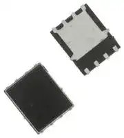


BSC004NE2LS5ATMA1
Power MOSFET, N Channel, 25 V, 479 A, 400 µohm, TDSON, Surface Mount
- Manufacturer: INFINEON
- Product type: Single MOSFETs
- SVHC: No SVHC (25-Jun-2025)
- No. of Pins: 8Pins
- Channel Type: N Channel
- Product Range: OptiMOS 5
- Qualification: -
- Power Dissipation: 188W
- Transistor Mounting: Surface Mount
- Rds(on) Test Voltage: 10V
- Transistor Case Style: TDSON
- Drain Source Voltage Vds: 25V
- Operating Temperature Max: 175°C
- Continuous Drain Current Id: 479A
- Drain Source On State Resistance: 400µohm
- Gate Source Threshold Voltage Max: 1.5V
| Delivery and price | |
|---|---|
| Units per pack | 1000 |
| Price | 1.19 € |
| Current stock | 200+ |
| Lead time | 30 days |
**BSC004NE2LS5**

## **MOSFET**

## **OptiMOS**

## **Features**

* Optimized for OR-ing application

_R_ DS(on) @ _V_ GS

|**Parameter**<br>~~Table~~ 1<br>~~Key Performance~~|**Value**<br>~~Performance Parameters~~|**Unit**<br>~~Parameters~~|
|---|---|---|
|_V_DS|25|V|
|_R_DS(on),max|0.45|mΩ|
|_I_D|479|A|
|_Q_oss|70|nC|
|_Q_G(0V..4.5V)|135|nC|


**==> picture [143 x 204] intentionally omitted <==**

**----- Start of picture text -----**<br>
8<br>7<br>6<br>OSE: ~ 5<br>“Agee,<br>1 < 5<br>2 6<br>3 4 ~~cS 7 8<br>4<br>3<br>2<br>1<br>S 1 ‘| : 8 D<br>S 2 7 D<br>S 3 | ( =) T C 6 D<br>G 4 5 D<br>**----- End of picture text -----**<br>


|~~Type/OrderingCode|~~|**Package**<br>~~||__|~~|**Marking**<br>~~|__|~~Related|Related Links|
|---|---|---|---|
|BSC004NE2LS5<br>~~Type/OrderingCode |~~|TDSON-8 FL<br>~~|~~|04NE2LS5<br>|-<br>|


Final Data Sheet

1

**OptiMOS[TM�] 5�Power-Transistor,�25�V BSC004NE2LS5**

**==> picture [120 x 53] intentionally omitted <==**

## **Table�of�Contents**

Description   . . . . . . . . . . . . . . . . . . . . . . . . . . . . . . . . . . . . . . . . . . . . . . . . . . . . . . . . . . . . . . . . . . . . . . . . . . . . . 1 Maximum ratings   . . . . . . . . . . . . . . . . . . . . . . . . . . . . . . . . . . . . . . . . . . . . . . . . . . . . . . . . . . . . . . . . . . . . . . . . 3 Thermal characteristics  . . . . . . . . . . . . . . . . . . . . . . . . . . . . . . . . . . . . . . . . . . . . . . . . . . . . . . . . . . . . . . . . . . . . 3 Electrical characteristics  . . . . . . . . . . . . . . . . . . . . . . . . . . . . . . . . . . . . . . . . . . . . . . . . . . . . . . . . . . . . . . . . . . . 4 Electrical characteristics diagrams  . . . . . . . . . . . . . . . . . . . . . . . . . . . . . . . . . . . . . . . . . . . . . . . . . . . . . . . . . . . 6 Package Outlines  . . . . . . . . . . . . . . . . . . . . . . . . . . . . . . . . . . . . . . . . . . . . . . . . . . . . . . . . . . . . . . . . . . . . . . . 10 Revision History  . . . . . . . . . . . . . . . . . . . . . . . . . . . . . . . . . . . . . . . . . . . . . . . . . . . . . . . . . . . . . . . . . . . . . . . . 12 Trademarks   . . . . . . . . . . . . . . . . . . . . . . . . . . . . . . . . . . . . . . . . . . . . . . . . . . . . . . . . . . . . . . . . . . . . . . . . . . . 12 Disclaimer   . . . . . . . . . . . . . . . . . . . . . . . . . . . . . . . . . . . . . . . . . . . . . . . . . . . . . . . . . . . . . . . . . . . . . . . . . . . . 12

Final Data Sheet

2

Rev.�2.0,��2020-04-23

**OptiMOS[TM�] 5�Power-Transistor,�25�V BSC004NE2LS5**

**==> picture [120 x 53] intentionally omitted <==**

**1�����Maximum�ratings** at� _T_ A=25�°C,�unless�otherwise�specified

## **Table�2�����Maximum�ratings**

|**Table2Maximumratings**|||||||
|---|---|---|---|---|---|---|
|**Parameter**|**Symbol**||**Values**||**Unit**|**Note/TestCondition**|
|||**Min.**|**Typ.**|**Max.**|||
|Continuous drain current1)|_I_D|-<br>-<br>-|-<br>-<br>-|479<br>338<br>40|A|_V_GS=10V,_T_C=25°C<br>_V_GS=10V,_T_C=100°C<br>_V_GS=4.5V,_T_A=25°C,<br>_R_THJA=50°C/W2)|
|Pulsed drain current3)|_I_D,pulse|-|-|1914|A|_T_A=25°C|
|Avalanche energy, single pulse4)|_E_AS|-|-|400|mJ|_I_D=30A,_R_GS=25Ω|
|Gate source voltage|_V_GS|-20|-|20|V|-|
|Power dissipation|_P_tot|-<br>-|-<br>-|188<br>2.5|W|_T_C=25°C<br>_T_A=25°C,_R_THJA=50°C/W2)|
|Operating and storage temperature|_T_j,_T_stg|-55|-|175|°C|IEC climatic category; DIN IEC 68-1:<br>55/175/56|


## **2�����Thermal�characteristics**

## **Table�3�����Thermal�characteristics**

|**Parameter**|**Symbol**||**Values**|**Values**|**Unit**|**Note/TestCondition**|
|---|---|---|---|---|---|---|
|||**Min.**|**Typ.**|**Max.**|||
|Thermal resistance, junction - case,<br>bottom|_R_thJC|-|-|0.8|°C/W|-|
|Thermal resistance, junction - case,<br>top|_R_thJC|-|-|20|°C/W|-|
|Device on PCB,<br>6 cm² cooling area|_R_thJA|-|-|50|°C/W|-|


> 1) Rating refers to the product only with datasheet specified absolute maximum values, maintaining case temperature at 25°C. For higher Tcase please refer to Diagram 2. De-rating will be required based on the actual environmental conditions.

> 2) Device on 40 mm x 40 mm x 1.5 mm epoxy PCB FR4 with 6 cm2 (one layer, 70 µm thick) copper area for drain connection. PCB is vertical in still air.

> 3) See Diagram 3 for more detailed information

> 4) See Diagram 13 for more detailed information

Final Data Sheet

3

Rev.�2.0,��2020-04-23

**OptiMOS[TM�] 5�Power-Transistor,�25�V BSC004NE2LS5**

**==> picture [120 x 53] intentionally omitted <==**

## **3�����Electrical�characteristics**

at� _T_ j=25�°C,�unless�otherwise�specified

## **Table�4�����Static�characteristics**

|**Parameter**|**Symbol**||**Values**|**Values**|**Unit**|**Note/TestCondition**|
|---|---|---|---|---|---|---|
|||**Min.**|**Typ.**|**Max.**|||
|Drain-source breakdown voltage|_V_(BR)DSS|25|-|-|V|_V_GS=0V,_I_D=1mA|
|Gate threshold voltage|_V_GS(th)|1|1.5|2|V|_V_DS=_V_GS,_I_D=10mA|
|Zero gate voltage drain current|_I_DSS|-<br>-|0.1<br>10|1<br>100|µA|_V_DS=20V,_V_GS=0V,_T_j=25°C<br>_V_DS=20V,_V_GS=0V,_T_j=125°C|
|Gate-source leakage current|_I_GSS|-|10|100|nA|_V_GS=16V,_V_DS=0V|
|Drain-source on-state resistance|_R_DS(on)|-<br>-|0.40<br>0.54|0.45<br>0.85|mΩ|_V_GS=10V,_I_D=30A<br>_V_GS=4.5V,_I_D=30A|
|Gate resistance|_R_G|-|0.7|-|Ω|-|
|Transconductance|_g_fs|-|230|-|S||_V_DS|≥2|_I_D|_R_DS(on)max,_I_D=30A|


## **Table�5�����Dynamic�characteristics**

|**Parameter**|**Symbol**||**Values**|**Values**|**Unit**|**Note/TestCondition**|
|---|---|---|---|---|---|---|
|||**Min.**|**Typ.**|**Max.**|||
|Input capacitance|_C_iss|-|11000|-|pF|_V_GS=0V,_V_DS=12.5V,_f_=1MHz|
|Output capacitance|_C_oss|-|3600|-|pF|_V_GS=0V,_V_DS=12.5V,_f_=1MHz|
|Reverse transfer capacitance|Crss|-|3100|-|pF|_V_GS=0V,_V_DS=12.5V,_f_=1MHz|
|Turn-on delay time|_t_d(on)|-|27.5|-|ns|_V_DD=12.5V,_V_GS=4.5V,_I_D=30A,<br>_R_G,ext=1.6Ω|
|Rise time|_t_r|-|88.2|-|ns|_V_DD=12.5V,_V_GS=4.5V,_I_D=30A,<br>_R_G,ext=1.6Ω|
|Turn-off delay time|_t_d(off)|-|67.6|-|ns|_V_DD=12.5V,_V_GS=4.5V,_I_D=30A,<br>_R_G,ext=1.6Ω|
|Fall time|_t_f|-|93.4|-|ns|_V_DD=12.5V,_V_GS=4.5V,_I_D=30A,<br>_R_G,ext=1.6Ω|


## **Table�6�����Gate�charge�characteristics[1)]**

|**Table6Gatechargecharacte**|**ristics1)**||||||
|---|---|---|---|---|---|---|
|**Parameter**|**Symbol**||**Values**||**Unit**|**Note/TestCondition**|
|||**Min.**|**Typ.**|**Max.**|||
|Gate to source charge|_Q_gs|-|24|-|nC|_V_DD=12.5V,_I_D=30A,_V_GS=0to4.5V|
|Gate charge at threshold|_Q_g(th)|-|15|-|nC|_V_DD=12.5V,_I_D=30A,_V_GS=0to4.5V|
|Gate to drain charge|_Q_gd|-|69|-|nC|_V_DD=12.5V,_I_D=30A,_V_GS=0to4.5V|
|Switchingcharge|_Q_sw|-|78|-|nC|_V_DD=12.5V,_I_D=30A,_V_GS=0to4.5V|
|Gate charge total|_Q_g|-|135|-|nC|_V_DD=12.5V,_I_D=30A,_V_GS=0to4.5V|
|Gate plateau voltage|_V_plateau|-|2.2|-|V|_V_DD=12.5V,_I_D=30A,_V_GS=0to4.5V|
|Gate charge total|_Q_g|-|238|-|nC|_V_DD=12.5V,_I_D=30A,_V_GS=0to10V|
|Output charge|_Q_oss|-|70|-|nC|_V_DS=12.5V,_V_GS=0V|


> 1) See ″ Gate charge waveforms ″ for parameter definition Final Data Sheet

Rev.�2.0,��2020-04-23

4

**OptiMOS[TM�] 5�Power-Transistor,�25�V BSC004NE2LS5**

**==> picture [120 x 53] intentionally omitted <==**

## **Table�7�����Reverse�diode**

|**Table7Reversediode**|||||||
|---|---|---|---|---|---|---|
|**Parameter**|**Symbol**||**Values**||**Unit**|**Note/TestCondition**|
|||**Min.**|**Typ.**|**Max.**|||
|Diode continuous forward current|_I_S|-|-|188|A|_T_C=25°C|
|Diode pulse current|_I_S,pulse|-|-|1914|A|_T_C=25°C|
|Diode forward voltage|_V_SD|-|0.77|1|V|_V_GS=0V,_I_F=30A,_T_j=25°C|
|Reverse recoverycharge|_Q_rr|-|30|-|nC|_V_R=12.5V,_I_F=_I_S,d_i_F/d_t_=400A/µs|


Final Data Sheet

Rev.�2.0,��2020-04-23

5

**OptiMOS BSC004NE2LS5**

**==> picture [538 x 289] intentionally omitted <==**

**----- Start of picture text -----**<br>
200 | | 500 ee ee<br>P N<br>175 —_N a<br>\ 400 N R r<br>\ a,<br>150<br>a NeNe ee ee ee<br>125 a eeNe<br>300 i a ee<br>i a<br>_ = a a<br>100 \ = eea eeee<br>\ 200 a ee ee ee<br>75 a ee<br>\ i a OTee ee<br>50 \ i<br>iA<br>100<br>25 \\ iaa eeeea ee<br>0 0 aai  ee eeeeeeeeee |e|<br>0 25 50 75 100 125 150 175 200 0 25 50 75 100 125 150 175 200<br>T C [°C] T C [°C]<br>P tot=f( T C) I D=f( T C V GS ≥<br>a ——OSOCOCOCOCSCSCSC“‘“#™#S<br>P tot I D<br>**----- End of picture text -----**<br>


**==> picture [527 x 283] intentionally omitted <==**

**----- Start of picture text -----**<br>
10 [4] 10 [1]<br>single pulse<br>0.01<br>EE tt 0.02 HEF<br>0.05<br>10 [3] ST 1 µs r 0.1 a<br>N S I 0.2 INTIME<br>10 µs<br>0.5<br>S S 10 [0] FETT FETT<br>ae 100 µs sees | M CI Hil<br>10 [2] A INNAHNHe HHHET THESIEHEHo e<br>BH 1 ms<br>TTT ONI N G ttTATT THT a SNE a | a IIE EIT<br>10 [1]<br>10 [-1]<br>10 ms<br>Saesersere | COBEAAICICI<br>DC<br>10 [0] ==rrSNSSeSON ll | e 2274ar a<br>ia TTee nea AETTAETM ET<br>ll<br>10 [-1] 10 [-2]<br>10 [-1] 10 [0] 10 [1] 10 [2] 10 [-5] 10 [-4] 10 [-3] 10 [-2] 10 [-1] 10 [0]<br>V DS [V] t p [s]<br>I D=f( V DS T C D t p Z thJC=f( t p D = t p/ T<br>I D thJC<br>Z<br>**----- End of picture text -----**<br>


Final Data Sheet

6

**OptiMOS BSC004NE2LS5**

**==> picture [531 x 633] intentionally omitted <==**

**----- Start of picture text -----**<br>
2000 1.4<br>10 V NV 5 V See) 2.8 V See 3 V 3.5 V<br>4.5 V<br>Lif POA<br>1750<br>tf / 1.2 fi)2Annee2000) Cee<br>) See<br>Ace<br>1500 | / / TTTELL 4 V Venue,A805Sae> 4eee42GedenseGeeseeee<br>7 1.0 BaP40S<br>p/p ee<br>1250 }-}/-5Lf) a CACPOCOeee A<br>0.8<br>_ // y ECOCCCCC CeCe eee 4 V<br>1000 / // ( e Coe<br>3.5 V 4.5 V<br>0.6<br>750 TLMerTTT oerSST 5 V<br>0.4 10 V<br>|W/}/fi PreeSoee<br>500<br>}/ Poo 3 V FEEEEEEEE<br>250 CepooIETEnAnHAEanAtl 2.8 V 0.2 PEPEECEEEE EEEeeeEEE eee EEEEEEEEEEECHEEEeee eee<br>Y a<br>yan F RE EE EE E ECEE eeeEe e e e  eeeeeeee<br>0 0.0<br>0.0 0.5 1.0 1.5 2.0 2.5 3.0 0 200 400 600 800 1000<br>V DS I D<br>[Vv] [A]<br>I D=f( V DS ), T j =25 °C; parameter: V GS R DS(on)=f( I D ), T j =25 °C; parameter: V GS<br>Diagram 7: Typ. transfer characteristics Diagram 8: Typ. drain-source on resistance<br>2000 ] 1.4 CCECEESSSSS08 OLE heeEEE EEE EEE LE LL<br>1750 / COCOA<br>25 °C 1.2<br>any SSSGe8 Cee<br>SSS008<br>175 °C a Ce<br>| / SSSSSe80) See<br>1500<br>I 1.0 BERERETA<br>/ / EOCCC CC( E s CHN E ETE E RREREIEREee<br>1250 | SSSSee<br>/ 0.8 PEE PSC EEE<br>175 °C<br>_< 1000 | / BEe FoeGoeeeeeceeeee erSS<br>7) See Ce<br>0.6<br>FREE Ce Cee NCEE EEE eee<br>VA FOC C ECC CONC Eee<br>750 ; FECEECCC<br>// CCE SCE 25 °C EEEeee<br>PEREFCCC ee<br>0.4<br>[ PCPC E ECPeeeeeeeeeeeeee eee) CERES<br>500<br>y, FRCP EEE eee eee e e e eeee<br>Y FEC C EEE Cee eee eee eee<br>y 0.2 FEEE EEE Cee ee eee eee eee<br>250<br>WYVA, EEEEEEEeee eeeee eeeeee<br>LYVV ECC P ERCEEPEECCeeee e eee eeeeee eee<br>0 0.0<br>0 1 2 3 4 5 0 2 4 6 8 10<br>V GS V GS<br>IV] IV]<br>I D=f( V GS V DS|>2| I D| R DS(on)max T j R DS(on)=f( V GS ),_=30 I D A; parameter: T j<br>] Ω<br>I D<br>DS(on)<br>R<br>] Ω<br>I D<br>DS(on)<br>R<br>**----- End of picture text -----**<br>


Final Data Sheet

7

**OptiMOS BSC004NE2LS5**

**==> picture [528 x 282] intentionally omitted <==**

**----- Start of picture text -----**<br>
2.0 PTT TITTLE LLL EEL 2.4 LL ET TT TTT TTT TTT TT EET<br>PELLET LE EET TEE TTT TET TET EET EET<br>Tee Aa LEE TET ETT TTT TET ET TTT EEE EE<br>2.0<br>1.6 TTT TT PA POOREST<br>PETIT a LEIA ET TTT EE ET ET ET TE EEE<br>7 [~~ = IN |<br>1.6<br>ite)° PECEELEEELEELELLE PEELE PITT TT TT TT [PASSE] ET TT<br>a 1.2 PCE AZ| LEE TET TTT TTT PNET~ PSMA~~<br>£ A PEE TET TET TTT ET ANEW EET<br>ha®PEELE 4Va EE percePN LAAN 100000 µA SRS<br>1.2<br>3E A N<br>5OP 0.8 POCdeenaPA FLTTISO TT TT TTT TT TT TTT TT ty 10000 µA rs<br>0.8<br>= PEPER FEET TT TTT TTT TT ET EET EET EE<br>LEE TET ETT TTT ET ETT EEE<br>0.4<br>TTT 0.4 PE EET TET TET ET EEE EE EE<br>ST PE ET TTT TTT TTT TET EET EET EET<br>PETE LEE TET ETT TTT ET TTTEEE<br>0.0 PETE TTT TEE E TEET E TTEE EEE E EEEELE] 0.0 PCCPFEEELEEEPTETELLE ELLE<br>-80 -40 0 40 80 120 160 200 -80 -40 0 40 80 120 160 200<br>T j [°C] T j [°C]<br>R DS(on)=f( T j I D V GS V GS(th=f( T j V GS= V DS I D<br>GS(th)<br>V<br>R<br>**----- End of picture text -----**<br>


**==> picture [530 x 283] intentionally omitted <==**

**----- Start of picture text -----**<br>
10 [5] 10 [4]<br>A A GG _<br>25 °C<br>EEE EEE EEE EEE EEE EE EEE ; [}-—-~~~~~~} ~~~<br>PEEEEEeeP eee eee et i 25 °C, max COE<br>BRR 1 175 °C FOE<br>SS ' 175 °C, max POPE<br>EEIEEEEEEEEEEEEREEEEEE or o<br>SUA ARUUAAAAMAGAANROAGAAIE EE E<br>PEELE EEE EEE 10 [3] TET vaileer<br>FREE ee<br>ELT BEER EEE EEE EEE EEEEE<br>Coss<br>¢— 10 [4] Ee ee eex fasiiastfasttaat/ J<br>rN TT TT TT yy yy Ciss y,<br>Qa Crss cat (anion ad<br>CNNSEER EEE PELLETA ee<br>Ltt EEE Eee 10 [2] /<br>HLNSS /<br>PCE SEEPREa PRRa ERER REESE REEa aER EEE REEES<br>ATLL ELEY] —a PEP errr eee<br>TT SEGRE RRR REG ee ee<br>10 [3] 10 [1]<br>0 5 10 15 20 25 0.00 0.25 0.50 0.75 1.00 1.25 1.50<br>V DS [V] V SD [V]<br>C =f( V DS V GS f I F=f( V SD T j<br>C I F<br>**----- End of picture text -----**<br>


Final Data Sheet

8

**OptiMOS BSC004NE2LS5**

**==> picture [528 x 283] intentionally omitted <==**

**----- Start of picture text -----**<br>
10 [2] 10<br>ee  ee oT<br>St 5 V TTT ITI TTI ITAL A<br>CT 1 12 V COO<br>Lr | TTTCi fT TT ETT TTT) 1 20 V RR 4a ‘ ane<br>a A A<br>8<br>CATION TIE NT EEE ECE<br>aa STN S EE<br>OLLIE<br>10 [1] PINE EER SNIP} EEEEEEEEEEEEE<br>25 °C<br>a a a ee ee eee 6 /| L<br>Te NEON TTT a Ae easae<br>= PTMICCOMILT TTT TENANT S PEPEPer<br>Ooo/\ 100 °C EECCALET TTT TTT TATPTT<br>4 LTTE TTT TTI YT AE PE EET TE<br>\ TT<br>10 [0] [ee ee = ee \ EEE eH<br>SSS y [|<br>a Nt 150 °C SCO<br>Lr | Ci Tt) 2 US snkJ |l| j//f\lyel to ee<br>SHH<br>HHH HH | GE /| SEEERPEEEEEE<br>LUTEAL AREERLPI TTT TTT TTT Ty ye yey yy TTT<br>10 [-1] EETI CUI | 0 AREER<br>10 [0] 10 [1] 10 [2] 10 [3] 10 [4] 0 40 80 120 160 200 240 280<br>t AV [us] Q gate [nC]<br>I AS=f( t AV R GS Ω T j,start V GS=f( Q gate I D T j V DD<br>I AV V GS<br>**----- End of picture text -----**<br>


**==> picture [537 x 301] intentionally omitted <==**

**----- Start of picture text -----**<br>
TT Diagram Gate charge waveforms<br>28<br>27 LEEVA py<br>AEE A<br>LEE<br>26<br>5 vA<br> UA<br>25<br>PETTERS<br>ALLEL<br>ELE<br>24<br>Sf<br>LL) ee ant<br>23<br>ATE | fc<br>-80 -40 0 40 80 120 160 200<br>T j [°C]<br>V BR(DSS)=f( T j I D OOCCTCTCTCTCTC—C*Y<br>BR(DSS)<br>V<br>**----- End of picture text -----**<br>


Final Data Sheet

9

**OptiMOS BSC004NE2LS5**

Final Data Sheet

10

**OptiMOS BSC004NE2LS5**

Final Data Sheet

11

**OptiMOS BSC004NE2LS5**

## BSC004NE2LS5

|Previous Revision|Previous Revision||
|---|---|---|
|Revision|Date|Subjects (major changes since last revision)|
|2.0|2020-04-23|Release of final version|


## **Trademarks**

## **erratum@infineon.com**

## **Information**

## **Warnings**

Final Data Sheet

12
Updated at April 29, 2026
Infineon Technologies is a globally recognized leader in semiconductor solutions, renowned for driving innovation in power management, energy efficiency, and modern mobility. With a strong legacy of engineering excellence, the company provides highly reliable components designed to meet the rigorous demands of industrial, automotive, and advanced commercial applications. The core of our Infineon portfolio is centered on their industry-leading discrete semiconductors. We offer an extensive selection of single and dual MOSFETs, alongside a robust range of single IGBTs and advanced IGBT modules. These flagship power transistors are essential for high-efficiency power conversion and motor control, providing engineers with superior thermal performance and minimized switching losses. Beyond advanced field-effect transistors, the selection includes a comprehensive array of diodes and rectifiers, heavily featuring Schottky diodes, as well as fast-recovery and RF/PIN diodes. This power foundation is further supported by bipolar transistors, intelligent power modules, and thyristor SCR modules, delivering the critical building blocks required for complex power system designs. To support broader system integration, the portfolio also encompasses specialized solutions such as solid-state relays, AC/DC LED driver ICs, and Bluetooth communications modules. From high-power industrial rectifiers to wireless connectivity adapters, Infineon equips designers with the precision components needed to build efficient, scalable, and fully connected electronic systems.
About Novapart
Novapart is a B2B electronic component broker specialising in stock shortages and cost reduction. We source hard-to-find parts and identify compliant alternatives across a catalogue of 410,000+ components from 500+ manufacturers.
Learn more →Stock Shortage Specialist
When a component is unavailable, discontinued or has an unacceptable lead time, we tap into our network of vetted European and Asian distributors to source what you need — without compromising on quality or traceability.
Request a quote →Compliant Alternatives
We identify pin-to-pin, electrically equivalent substitutes that meet the same certifications (RoHS, AEC-Q100, REACH) as your original specification — validated against datasheets, not just part numbers. Often at a lower cost.
BOM Analysis service →