
Image not available
Illustrative purposes only

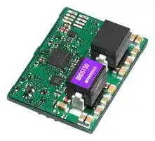
BRDS150
Non Isolated POL DC/DC Converter, ITE, Non Isolated POL, 600 mV, 1.8 V, 150 A
⚠️ Reference pricing provided. In case of supply shortages, we will connect you with our trusted procurement partners to ensure your project's continuity.
- Manufacturer: COSEL
- Product type: DC / DC Non Isolated Board Mount Converters - Adjustable Output
- SVHC: To Be Advised
- Depth: 38mm
- Width: 27.7mm
- Height: 13.8mm
- Product Range: BRDS Series
- Output Power Max: -
- Output Current Max: 150A
- Output Voltage Max: 1.8V
- Output Voltage Min: 600mV
- Input Voltage DC Max: 14V
- Input Voltage DC Min: 4.5V
- DC / DC Converter Type: Non Isolated POL
- Power Supply Applications: ITE
- DC / DC Converter Output Type: Fixed
| Delivery and price | |
|---|---|
| Units per pack | 50 |
| Price | 76.77 € |
| Current stock | 10+ |
| Lead time | 30 days |
Datasheet

**DC-DC Converters POL Type** Low Profile Safety OCP Remote Approvals ON/OFF

## **BRFS/BRDS-series**

## **Feature**

Small size and high efficiency non-isolated DC-DC converter.

Wide input voltage 4.5V to 14.0V.

Fast transient respoce by Robust control.

Built-in remote ON/OFF,Power good,Start-up sequence.

Built-in overcurrent and thermal protection (auto recovery type) functions.

PMBus interface for programming, margining, and telemetry (BRDS-series).

## **CE marking**

Low Voltage Directive RoHS Directive

## **UKCA marking**

Electrical Equipment Safety Regulations RoHS Regulations

## **Safety agency approvals**

UL60950-1, C-UL, EN62368-1

## **5-year warranty**

**BRFS/BRDS-1**

www.cosel.co.jp/en/

August 02, 2023

~~eS~~

**DC-DC Converters POL Type BRFS**

**==> picture [87 x 8] intentionally omitted <==**

**----- Start of picture text -----**<br>
Ordering information<br>**----- End of picture text -----**<br>


**==> picture [2 x 3] intentionally omitted <==**

**----- Start of picture text -----**<br>
R<br>**----- End of picture text -----**<br>


**==> picture [237 x 204] intentionally omitted <==**

**----- Start of picture text -----**<br>
-<br>BRF  S  60  S  O<br>1� 2� 3� 4� 5<br>1Series name<br>2Single output<br>3Output current<br> 30:30A<br> 40:40A<br> 60:60A<br> 100:100A<br> 120:120A<br> 150:150A<br>4Type<br>Blank : Standard type<br>S  : Small type (only 60A)<br>5Optional<br>x7 a a  R : Positive logic remote<br>    on/off<br>  I : POWERGOOD<br>   (only BRFS30/40/60S)<br>. er models has POWERGOOD<br>function normally.<br> P : Parallel operation<br>   (only BRFS40/60S)<br>Y1 : Fast transient response<br>}    (only BRFS100)<br>**----- End of picture text -----**<br>


|~~GG~~|**MODEL**<br>~~GG~~|**BRFS30**<br>~~GG~~|**BRFS40**<br>~~GG~~|**BRFS60**|**BRFS60S**<br>~~CO~~|**BRFS100**<br>~~CO~~|**BRFS120**<br>~~CO~~|**BRFS150**|
|---|---|---|---|---|---|---|---|---|
|**INPUT**<br>~~Po~~<br>~~ee~~<br>~~GG~~<br>~~po~~|**VOLTAGE[V]**<br>~~Po~~<br>~~ee~~|DC4.5 - 14.0<br>~~GeGO~~|||||||
||**CURRENT[A]**<br>*1 <br>~~ee~~|3.41 typ<br>~~Ge~~|4.52 typ<br>~~Ge~~|6.82 typ<br>~~GO~~|6.71 typ<br>~~GO~~|11.24 typ<br>~~GO~~|13.50 typ<br>~~GO~~|16.90 typ|
||**EFFICIENCY[%]**<br>*1 <br>~~ee~~<br>~~GG~~<br>~~po~~|88.0 typ<br>~~Ge~~<br>~~GG~~|88.5 typ<br>~~Ge ~~<br>~~GG~~|88.0 typ<br> ~~GO~~<br>~~GG~~|89.5 typ<br>~~GO~~<br>~~GG~~<br>~~GO~~|89.0 typ<br>~~GO~~<br>~~GG~~<br>~~GO~~|89.0 typ<br>~~GO~~<br>~~GG~~|89.0 typ|
|**OUTPUT**<br>~~GG~~<br>~~po~~<br>~~Po~~<br>~~Po~~<br>~~po~~<br>~~po~~<br>~~po~~<br>~~Po~~<br>~~a~~<br>~~ee~~<br>~~Po~~|**VOLTAGE[V]**<br>*2 <br>~~GG~~<br>~~po~~|0.8 - 3.63<br>~~GG~~|0.6 - 2.0<br>~~GG~~|0.7 - 2.0<br>~~GG~~|0.6 - 2.0<br>~~GG~~<br>~~GO~~|0.7 - 2.0<br>~~GG~~<br>~~GO~~|0.6 - 1.8<br>~~GG~~|0.6 - 1.8*7|
||**CURRENT[A]**<br>~~po~~|30|40|60|60<br>~~GO~~|100<br>~~GO~~|120|150|
||**LINE REGULATION[mV]**<br>~~po~~<br>~~Po~~|5<br>~~GO~~|||||||
||**LOAD REGULATION[mV]**<br>~~Po~~|5|||||||
||**RIPPLE[mVp-p]**<br>*3 <br>~~po~~|25|||||||
||**RIPPLE NOISE[mVp-p]**<br>*3 <br>~~po~~|50|||||||
||**OUTPUT VOLTAGE SETTING [%Vo]**<br>~~po~~|±1|||||||
||**DRIFT[mV]**<br>*4 <br>~~Po~~|5|||||||
||**START-UP TIME[ms]**<br>~~a~~<br>~~ee~~|8.0 typ<br>~~cee~~<br>~~eesees~~|||12.0 typ *6<br>~~eee~~|8.0 typ<br>~~eee~~|12.0 typ *6<br>~~eee~~||
||**OUTPUT VOLTAGE[V]**<br>**ADJUSTMENT RANGE**<br>~~ee~~|Adjustable byexternal resistor<br>~~cee~~<br>~~eeseeseeeeee~~|||||||
|||0.8 - 3.63<br>~~cee~~|0.6 - 2.0<br>~~ees~~|0.7 - 2.0<br>~~ees~~|0.6 - 2.0<br>~~eee~~|0.7 - 2.0<br>~~eee~~|0.6 - 1.8<br>~~eee~~|0.6 - 1.8*7|
||**OUTPUT VOLTAGE TOTAL REGULATION [%Vo]***5 <br>~~ee ~~<br>~~Po~~|±3<br> ~~cee~~<br>~~ees ees eee eee~~|||||||
|**PROTECTION**<br>**CIRCUIT AND**<br>**OTHERS**<br>~~po~~<br>~~ee~~<br>~~Po~~|**OVERCURRENT PROTECTION**<br>~~po~~|Works over 105% of rating (auto recoverytype)|||||||
||**REMOTE SENSING**<br>~~ee~~|Available(+S only)<br>~~ee~~||Available<br>~~ee~~|Available (+S only)<br>~~ee~~|Available|||
||**REMOTE ON/OFF**<br>~~Po~~|Available Negative logic L:ON, H:OFF|||||||
|**ISOLATION**<br>~~Po~~<br>~~Pp~~|**INPUT-OUTPUT**<br>~~Po~~<br>~~Pp~~|non-isolated|||||||
|**ENVIRONMENT**<br>~~Pppo~~<br>~~Po~~<br>~~Po~~|**OPERATING TEMP.,HUMID.AND ALTITUDE**<br>~~Pp~~|-40 to +85C, 20-95%RH(Non condensing) (Refer to “Derating”)3,000m(10,000feet)max|||||||
||**STORAGE TEMP.,HUMID.AND ALTITUDE**<br>~~Pppo~~|-40 to +100C, 20-95%RH(Non condensing), 9,000m(30,000feet)max|||||||
||**VIBRATION**<br>~~Po~~|10-55Hz, 49.0m/s2 (5G), 3minutesperiod, 60minutes each alongX, Y and Z axis|||||||
||**IMPACT**<br>~~Po~~|196.1m/s2 (20G), 11ms, once each alongX, Y and Z axis|||||||
|**SAFETY**<br>~~Po~~|**AGENCY APPROVALS**<br>~~Po~~|UL60950-1, C-UL(CSA60950-1), EN62368-1|||||||
|**OTHERS**<br>~~Pp~~|**CASE SIZE/WEIGHT**<br>~~Pp~~|33.0X9.5X13.5mm<br>[1.3X0.37X0.53<br>inches] (WXHXD) /<br>10gmax|33.0X10.9X13.5mm<br>[1.3X0.43X0.53<br>inches] (WXHXD) /<br>12gmax|33.0X8.0X22.9mm<br>[1.3X0.31X0.9<br>inches] (WXHXD) /<br>15gmax|33.0X12.7X13.5mm<br>[1.3X0.5X0.53<br>inches] (WXHXD) /<br>12gmax|38.0X8.5X27.7mm<br>[1.5X0.33X1.09<br>inches] (WXHXD) /<br>22gmax|33.0X12.7X22.9mm<br>[1.3X0.5X0.9<br>inches] (WXHXD) /<br>14gmax|38.0X13.8X27.7mm<br>[1.5X0.54X1.09<br>inches] (WXHXD) /<br>21gmax|
||**COOLING METHOD**<br>~~Pp~~|Convection / Forced air|||||||


- *1 At rated input (DC12V) and rated output (1.2V) Ta=25C.

- *2 Output voltage is adjusted to the minimum when TRM is opened.

- *3 Ripple and ripple noise is measured by using measuring board with  ceramic capacitor at 50mm from output pin.

- *4 Drift is the change in DC output for an eight hour period after a half - hour warm - up at 25C, with the input voltage held.

- *5 Output voltage setting is added line regulation and load regulation and temperature regulation used resistance of the 0.5% tolerance.

- *6 The start-up time when using the RC terminal is same as other BRFS.

- *7 The output voltage adjustment area determines by the input voltage.

**BRFS/BRDS-2**

www.cosel.co.jp/en/

August 02, 2023

## **BRFS**

## **External view**

**==> picture [477 x 430] intentionally omitted <==**

**----- Start of picture text -----**<br>
1. BRFS30 6.0 [    0.236]  max to a center 2. BRFS40 8.0 [    0.315]  max to a center<br>(adsorption area)<br>(adsorption area) 33±0.5<br>9.95±0.5 [1.299]33±0.5 20.3±0.5 [1.299]<br>[0.392] [0.799]<br>Name Plate Name Plate<br>Coplanarity within 0.1<br>Coplanarity within 0.1<br>1.22 30.58 [1.204] 2-   1.6 1.22 30.58 [1.204] 7-   1.6<br>[0.048] 29.90 [1.177]  [    0.063] [0.048] 29.90 [1.177]  [    0.063]<br>RC +VIN RC +VIN<br>SGND GND SGND GND<br>NC (option : PGOOD) NC (option : PGOOD/SHARE)<br>+S TRM +VOUT GND SEQ +S TRM +VOUT GND SEQ<br>2.72 8-2.7×1.6 2.72 3-2.7×1.6<br>[0.107] 7.54 [0.297] [0.106×0.063] [0.107] 7.54 [0.297] [0.106×0.063]<br>12.37 [0.487] 12.37 [0.487]<br>17.20 [0.677] 17.20 [0.677]<br>22.02 [0.867] 22.02 [0.867]<br>26.85 [1.057] 26.85 [1.057]<br>Tolerance : ±0.3 [±0.012] Tolerance : ±0.3 [±0.012]<br>Dimensions in mm, [    ]=inches  Dimensions in mm, [    ]=inches<br>Weight : 10g max Weight : 12g max<br>Terminal material : copper   Terminal material : copper<br>Plating treatment of terminal Plating treatment of terminal<br> : Lead free plating   : Lead free plating<br>±0.5 0.5<br>6.85 [0.270] 6.85± [0.270]<br>±0.5 0.5<br>13.5 [0.531] 13.5± [0.531]<br>9.5max [0.374] 10.9max [0.429]<br>1.91 [0.075] 1.91 [0.075]<br>0.64 [0.025] 0.64 [0.025]<br>[0.405] [0.405]<br>3.05 [0.120] 2.26 [0.089] 3.05 [0.120] 2.26 [0.089]<br>10.29 10.29<br>**----- End of picture text -----**<br>


**==> picture [217 x 154] intentionally omitted <==**

**----- Start of picture text -----**<br>
Recommended size for processing PCB<br>TOP VIEW<br>26.85 [1.057]<br>22.02 [0.867]<br>17.20 [0.677]<br>12.37 [0.487]<br>7.54 [0.297]<br>2.72 [0.107] 7-3.56×2.41<br> [0.140×0.095]<br>29.90 [1.177]<br>30.58 [1.204] 2-2.41×2.08<br> [0.095×0.082]<br>3.40×2.41<br> [0.134×0.095] Dimension is : mm [inch]<br>2.26 [0.089]<br>10.29 [0.405] 0.64 [0.025]<br>3.05 [0.120] 0.08 [0.003]<br>**----- End of picture text -----**<br>


**BRFS/BRDS-3**

www.cosel.co.jp/en/

August 02, 2023

## **BRFS**

## **External view**

**==> picture [241 x 381] intentionally omitted <==**

**----- Start of picture text -----**<br>
3. BRFS60<br>33±0.5     11.0 [   0.433] max<br>23.4±0.5 [1.299]  to a center<br>[0.921] (adsorption area)<br>Name Plate<br>Coplanarity within 0.1<br>29.72 [1.170]<br>23.12 [0.910]<br>16.54 [0.651]<br>13.16 [0.518]<br>6.58<br>1.63 [0.064] [0.259] 6-    2.3<br> [    0.091]<br>+VIN GND +VOUT +VOUT GND +VIN<br>8-   1.6<br>SHARE  [    0.063]<br>-TRM +TRM +S -S RC PGOOD SEQ<br>0.13<br>[0.005] 4.27 [0.168]<br>8.56 [0.337]<br>12.86 [0.506]<br>17.12 [0.674]<br>21.42 [0.843]<br>25.68 [1.011]<br>29.98 [1.180]<br>0.5<br>8.1± [0.319]<br>0.5<br>22.9± [0.902]<br>8.0max [0.315]<br>1.91 [0.075]<br>19.43 [0.765]<br>**----- End of picture text -----**<br>


**==> picture [190 x 193] intentionally omitted <==**

**----- Start of picture text -----**<br>
Recommended size for processing PCB<br>TOP VIEW<br>29.98 [1.180]<br>25.68 [1.011]<br>21.42 [0.843]<br>17.12 [0.674]<br>12.86 [0.506]<br>8.56 [0.337]<br>4.27 [0.168]<br>0.13 [0.005]<br>8-    2.39<br> [    0.094]<br>6.58 [0.259]<br>13.16 [0.518] 6-    3.12<br>16.54 [0.651]  [    0.123]<br>23.12 [0.910]<br>29.72 [1.170]<br>Dimension is : mm [inch]<br>19.43 [0.765]<br>**----- End of picture text -----**<br>


Tolerance : ±0.3 [±0.012] Dimensions in mm, [    ]=inches Weight : 15g max Terminal material : copper Plating treatment of terminal : Lead free plating

**BRFS/BRDS-4**

www.cosel.co.jp/en/

August 02, 2023

## **BRFS**

## **External view**

## 4. BRFS60S

**==> picture [489 x 655] intentionally omitted <==**

**----- Start of picture text -----**<br>
33±0.5 Recommended size for processing PCB<br>20.2±0.5 [1.299]    8.0(adsorption area)[   0.315] max to a center TOP VIEW<br>[0.795]<br>26.85 [1.057]<br>22.02 [0.867]<br>17.2 [0.677]<br>12.37 [0.487]<br>7.54 [0.297] 8-3.56×2.41<br>2.72 [0.107] [0.140×0.095]<br>Name Plate<br>29.9 [1.177]<br>Coplanarity within 0.1<br>1.22<br>[0.048] 29.9 [1.177] 2.41×2.08<br>3.40×2.41 [0.095×0.082]<br>RC +VIN [0.134×0.095] Dimension is : mm [inch]<br>SGND GND<br>NC ( オプション: PGOOD/SHARE)<br>+S TRM +VOUT GND SEQ Tolerance : ±0.3 [±0.012]<br>Dimensions in mm, [    ]=inches<br>2.72 [0.107] 6-   1.6 Weight : 12g max<br>7.54 [0.297] [   0.063] Terminal material : copper<br>12.37 [0.487] 4-2.7×1.6 Plating treatment of terminal<br>17.2 [0.677] [   0.106×0.063]  : Lead free plating<br>22.02 [0.867]<br>26.85 [1.057]<br>5. BRFS100<br>    11.0 [   0.433] max to a center<br>38±0.5<br>29.95±0.5 [1.496] (adsorption area) Recommended size for processing PCB<br>[1.179] TOP VIEW<br>29.98 [1.180]<br>25.68 [1.011]<br>21.42 [0.843]<br>17.12 [0.674]<br>12.86 [0.506]<br>8.56 [0.337]<br>4.27 [0.168]<br>0.13 [0.005]<br>Name Plate 8-    2.39<br> [    0.094]<br>Coplanarity within 0.1<br>29.72 [1.170]<br>23.12 [0.910] 6.58 [0.259] 12-    3.12<br>16.54 [0.651] 13.16 [0.518]  [    0.123]<br>13.16 [0.518] 12-    2.3 16.54 [0.651]<br>23.12 [0.910]<br>4.15 6.58  [    0.091] 29.72 [1.170]<br>[0.163] [0.259]<br>Dimension is : mm [inch]<br>+VIN GND +VOUT +VOUT GND +VIN<br>+VIN GND +VOUT +VOUT GND +VIN<br>Tolerance : ±0.3 [±0.012]<br>Dimensions in mm, [    ]=inches<br>Weight : 22g max<br>8-   1.6 Terminal material : copper<br> [    0.063] Plating treatment of terminal<br> : Lead free plating<br>SHARE -TRM +TRM +S -S RC PGOOD SEQ<br>0.13[0.005]<br>4.27 [0.168]<br>8.56 [0.337]<br>12.86 [0.506]<br>17.12 [0.674]<br>21.42 [0.843]<br>25.68 [1.011]<br>29.98 [1.180]<br>0.5<br>6.85± [0.270]<br>0.5<br>13.5± [0.531]<br>2.26 [0.089]<br>12.7max [0.500] 10.29 [0.405] 0.64 [0.025]<br>911. [0.075] 4 3.05 [0.120] 0.0030.08 ][<br>0.6 [0.025]<br>[0.405]<br>3.05 [0.120] 2.26 [0.089]<br>10.29<br>0.5<br>±<br>86. [0.268]<br>0.5<br>27.7± [1.091]<br>[0.954]<br>ax<br>85m. [0.335] 24.23 [0.133]<br>3.38<br>[0.075]<br>1<br>9<br>1.<br>[0.133]<br>[0.954]3 383.<br>24.2<br>**----- End of picture text -----**<br>


**BRFS/BRDS-5**

www.cosel.co.jp/en/

August 02, 2023

## **BRFS**

## **External view**

**==> picture [504 x 655] intentionally omitted <==**

**----- Start of picture text -----**<br>
6. BRFS120 23.3±[0.917]0.5 33.0±[1.299]0.5 (adsorption area)7.0to a center[    0.276]  max  7. BRFS150 27.3±[1.075]0.5 38.0±[1.496]0.5 (adsorption area)7.0to a center[    0.276]  max<br>Name Plate<br>Name Plate<br>Coplanarity<br>within 0.1<br>29.72 [1.170] Coplanarity<br>23.12 [0.910] within 0.1<br>16.54 [0.651] 29.72 [1.170]<br>13.16 [0.518] 23.12 [0.910]<br>6.58 16.54 [0.651]<br>1.63 [0.064] [0.259] 6-   2.3 13.16 [0.518] 12-   2.3<br> [    0.091] 4.15 6.58  [    0.091]<br>[0.163] [0.259]<br>+VIN GND +VOUT +VOUT GND +VIN<br>+VIN GND +VOUT +VOUT GND +VIN<br>+VIN GND +VOUT +VOUT GND +VIN<br>SHARE<br>-TRM +TRM +S -S RC PGOOD SEQ 8-   1.6<br> [    0.063]<br>0.13 [0.005]<br>4.27 [0.168] 8-   1.6 SHARE -TRM +TRM +S -S RC PGOOD SEQ<br>8.56 [0.337]  [    0.063]<br>12.86 [0.506]<br>17.12 [0.674] 0.13 [0.005]<br>21.42 [0.843] 4.27 [0.168]<br>25.68 [1.011] 8.56 [0.337]<br>29.98 [1.180] 12.86 [0.506]<br>17.12 [0.674]<br>21.42 [0.843]<br>25.68 [1.011]<br>29.98 [1.180]<br>Tolerance : ±0.3 [±0.012] Tolerance : ±0.3 [±0.012]<br>Dimensions in mm, [    ]=inches  Dimensions in mm, [    ]=inches<br>Weight : 14g max Weight : 21g max<br>Terminal material : copper   Terminal material : copper<br>Plating treatment of terminal Plating treatment of terminal<br>: Lead free plating   : Lead free plating<br>Recommended size for processing PCB Recommended size for processing PCB<br>TOP VIEW TOP VIEW<br>29.98 [1.180] 29.98 [1.180]<br>21.42 25.68 [0.843[1.011] ] 17.12 21.42 [25.68 0.674[0.843][1.011] ]<br>17.12 [0.674] 12.86 [0.506]<br>12.86 [0.506] 8.56 [0.337]<br>8.56 [0.337] 4.27 [0.168]<br>4.27 [0.168] 0.13 [0.005]<br>0.13 [0.005] 8-   2.39<br>[   0.094]<br>8-   2.39<br>[   0.094]<br>6.58 [0.259] 6-   3.12<br>13.16 [0.518] [   0.123] 6.58 [0.259] 12-   3.12<br>16.54 [0.651] 13.16 [0.518] [   0.123]<br>23.12 [0.910] 16.54 [0.651]<br>29.72 [1.170] 23.12 [0.910]<br>29.72 [1.170]<br>Dimension is : mm [inch]<br>Dimension is : mm [inch]<br>15.4±0.5 [0.606] 20.6±0.5 [0.811]<br>0.5<br>0.5 27.7± [1.091]<br>22.9± [0.902]<br>[0.500]<br>12.7max<br>[0.543]<br>13.8max<br>[0.075]<br>1.91<br>] 1 0.075][<br>0.765[ 91. ]<br>]<br>0.133[<br>19.43  0.954[<br>3.38<br>24.23<br>24.23 [0.954]<br>19.43 [0.765]<br>3.38 [0.133]<br>**----- End of picture text -----**<br>


**BRFS/BRDS-6**

www.cosel.co.jp/en/

August 02, 2023

## **BRFS**

**BRFS/BRDS-7**

www.cosel.co.jp/en/

August 02, 2023

**==> picture [2 x 3] intentionally omitted <==**

**----- Start of picture text -----**<br>
R<br>**----- End of picture text -----**<br>


**==> picture [415 x 158] intentionally omitted <==**

**----- Start of picture text -----**<br>
DC-DC Converters POL Type Ordering information<br>-<br>BRD  S  100  O O<br>BRDS<br>1� 2� 3� 4� 5<br>1Series name<br>2Single output<br>3Output current<br> 40:40A<br> 60:60A<br> 100:100A<br> 120:120A<br> 150:150A<br>4Type<br> Blank : Standard type<br>2S ££  S : Small type (Only 60A)<br>5Optional<br> R : Positive logic remote<br>    on/off<br>**----- End of picture text -----**<br>


|~~GD~~|**MODEL**<br>~~GD~~|**BRDS40**<br>~~GD~~|**BRDS60**<br>~~GD~~|**BRDS60S**<br>~~GD~~|**BRDS100**<br>~~GD~~|**BRDS120**<br>~~GD~~|**BRDS150**|
|---|---|---|---|---|---|---|---|
|**INPUT**<br>~~Po~~<br>~~ee~~<br>~~Re~~<br>~~a~~|**VOLTAGE[V]**<br>~~Po~~|DC4.5 - 14.0||||||
||**CURRENT[A]**<br>*1 <br>~~ee~~<br>~~Re~~|4.52 typ<br>~~ee~~|6.82 typ<br>~~ee~~|6.71 typ<br>~~ee~~|11.24 typ<br>~~ee~~|13.50 typ<br>~~ee~~|16.90 typ|
||**EFFICIENCY[%]**<br>*1 <br>~~Re~~<br>~~a~~|88.5 typ<br>~~Ge~~|88.0 typ|89.5 typ<br>~~OO~~|89.0 typ<br>~~OO~~|89.0 typ|89.0 typ|
|**OUTPUT**<br>~~Re~~<br>~~a~~<br>~~a~~<br>~~Po~~<br>~~Po~~<br>~~Po~~<br>~~Po~~<br>~~Po~~<br>~~Po~~<br>~~Po~~<br>~~Be~~<br>~~Po~~|**VOLTAGE[V]**<br>*2 <br>~~Re~~<br>~~a~~<br>~~a~~|0.6 - 2.0<br>~~Ge~~<br>~~Pe~~|0.7 - 2.0|0.6 - 2.0<br>~~OO~~|0.7 - 2.0<br>~~OO~~|0.6 - 1.8|0.6 - 1.8*6|
||**CURRENT[A]**<br>~~a~~<br>~~a~~|40<br>~~Ge~~<br>~~Pe~~|60|60<br>~~OO~~|100<br>~~OO~~|120|150|
||**LINE REGULATION[mV]**<br>~~a~~<br>~~Po~~|5<br>~~Pe~~||||||
||**LOAD REGULATION[mV]**<br>~~Po~~|5||||||
||**RIPPLE[mVp-p]**<br>*3 <br>~~Po~~|25||||||
||**RIPPLE NOISE[mVp-p]**<br>*3 <br>~~Po~~|50||||||
||**OUTPUT VOLTAGE SETTING [%Vo]**<br>~~Po~~|±1||||||
||**DRIFT[mV]**<br>*4 <br>~~Po~~|5||||||
||**START-UP TIME[ms]**<br>~~Po~~<br>~~Be~~|12.0 typ||||||
||**OUTPUT VOLTAGE[V]**<br>**ADJUSTMENT RANGE**<br>~~Be~~|Adjustable byexternal resistor||||||
|||0.6 - 2.0|0.7 - 2.0|0.6 - 2.0|0.7 - 2.0|0.6 - 1.8|0.6 - 1.8*6|
||**OUTPUT VOLTAGE TOTAL REGULATION [%Vo]***5 <br>~~Be~~<br>~~Po~~|±3||||||
|**PROTECTION**<br>**CIRCUIT AND**<br>**OTHERS**<br>~~Po~~<br>~~Po~~<br>~~Po~~|**OVERCURRENT PROTECTION**<br>~~Po~~|Works over 105% of rating (auto recoverytype)||||||
||**REMOTE SENSING**<br>~~Po~~|Available||||||
||**REMOTE ON/OFF**<br>~~Po~~|Available Negative logic L:ON, H:OFF||||||
|**ISOLATION**<br>~~Po~~|**INPUT-OUTPUT**<br>~~Po~~|non-isolated||||||
|**ENVIRONMENT**<br>~~Po~~<br>~~Po~~<br>~~Po~~<br>~~Po~~|**OPERATING TEMP.,HUMID.AND ALTITUDE**<br>~~Po~~|-40 to +85C, 20-95%RH(Non condensing) (Refer to “Derating”)3,000m(10,000feet)max||||||
||**STORAGE TEMP.,HUMID.AND ALTITUDE**<br>~~Po~~|-40 to +100C, 20-95%RH(Non condensing), 9,000m(30,000feet)max||||||
||**VIBRATION**<br>~~Po~~|10-55Hz, 49.0m/s2 (5G), 3minutesperiod, 60minutes each alongX, Y and Z axis||||||
||**IMPACT**<br>~~Po~~|196.1m/s2 (20G), 11ms, once each alongX, Y and Z axis||||||
|**SAFETY**<br>~~Po~~|**AGENCY APPROVALS**<br>~~Po~~|UL60950-1, C-UL(CSA60950-1), EN62368-1||||||
|**OTHERS**<br>~~Pp~~|**CASE SIZE/WEIGHT**<br>~~Pp~~|33.0X10.9X13.5mm<br>[1.3X0.43X0.53<br>inches] (WXHXD) /<br>12gmax|33.0X8.0X22.9mm<br>[1.3X0.31X0.9<br>inches] (WXHXD) /<br>15gmax|33.0X12.7X13.5mm<br>[1.3X0.5X0.53<br>inches] (WXHXD) /<br>12gmax|38.0X8.5X27.7mm<br>[1.5X0.33X1.09<br>inches] (WXHXD) /<br>22gmax|33.0X12.7X22.9mm<br>[1.3X0.5X0.9<br>inches] (WXHXD) /<br>14gmax|38.0X13.8X27.7mm<br>[1.5X0.54X1.09<br>inches] (WXHXD) /<br>21gmax|
||**COOLING METHOD**<br>~~Pp~~|Convection / Forced air||||||


- *1 At rated input (DC12V) and rated output (1.2V) Ta=25C.

- *2 Output voltage is adjusted to the minimum when TRM is opened.

- *3 Ripple and ripple noise is measured by using measuring board with  ceramic capacitor at 50mm from output pin.

- *4 Drift is the change in DC output for an eight hour period after a half - hour warm - up at 25C, with the input voltage held.

- *5 Output voltage setting is added line regulation and load regulation and temperature regulation used resistance of the 0.5% tolerance.

- *6 The output voltage adjustment area determines by the input voltage.

- This product is subject to a license from PAI Capital LLC related to digital power technology patents owned by PAI Capital LLC.

**BRFS/BRDS-8**

www.cosel.co.jp/en/

August 02, 2023

## **BRDS**

## **External view**

**==> picture [232 x 431] intentionally omitted <==**

**----- Start of picture text -----**<br>
1. BRDS40<br>8.0 [    0.315]  max<br>33±0.5 to a center<br>20.3±0.5 [1.299] (adsorption area)<br>[0.799]<br>Name Plate<br>Coplanarity<br>within 0.1<br>1.22 30.58 [1.204]<br>[0.048]<br>29.9 [1.177]<br>17.93 [0.706]<br>10.95 [0.431]<br>5.84<br>3.05 [0.230]<br>[0.120]<br>ADDR1 16-   1.6<br> [    0.063]<br>RC +VIN<br>SGND SGNDADDR0 SMBALERT PGOOD GND<br>-S CLK DATA NC<br>SHARE +S TRM +VOUT GND SEQ<br>2.72<br>[0.107] 7.54[0.297] 3-2.7×1.6<br>[0.106×0.063]<br>12.37 [0.487]<br>17.20 [0.677]<br>22.02 [0.867]<br>26.85 [1.057]<br>Tolerance : ±0.3 [±0.012]<br>Dimensions in mm, [    ]=inches<br>Weight : 12g max<br>Terminal material : copper<br>Plating treatment of terminal<br>: Lead free plating<br>0.5<br>0.5 6.85± [0.270]<br>13.5± [0.531]<br>10.9max [0.429]<br>1.91 [0.075] 3.05 0.120][ 2.26 [0.089]<br>6.47 [0.255] 4.95 [0.195] 0.64 [0.025]<br>10.29 [0.405]<br>**----- End of picture text -----**<br>


**==> picture [204 x 204] intentionally omitted <==**

**----- Start of picture text -----**<br>
Recommended size for processing PCB<br>TOP VIEW<br>26.85 [1.057]<br>22.02 [0.867]<br>17.20 [0.677]<br>12.37 [0.487]<br>7.54 [0.297] 7-3.56×2.41<br>8-2.39×2.39 2.72 [0.107]  [0.140×0.095]<br> [0.094×0.094] 3-2.41×2.08<br> [0.095×0.082]<br>3.05<br>[0.120]<br>3.40×2.41 5.84<br> [0.134×0.095] [0.230]<br>10.95 [0.431]<br>1.22 [0.048] 17.93 [0.706]<br>29.9 [1.177]<br>30.58 [1.204]<br>Dimension is : mm [inch]<br>10.29 [0.405] 6.47 [0.255]<br>1.91 [0.075] 3.05 [0.120] 0.08 [0.003] 2.26 [0.089] 4.95 [0.195] 0.64 [0.025]<br>**----- End of picture text -----**<br>


**==> picture [246 x 663] intentionally omitted <==**

**----- Start of picture text -----**<br>
2. BRDS60S<br>33±0.5 8.0 [    0.315]  max<br>to a center<br>20.2±0.5 [1.299] (adsorption area)<br>[0.795]<br>Name Plate<br>Coplanarity<br>within 0.1<br>1.22 [0.048] 30.58 [1.204]<br>29.9 [1.177]<br>17.93 [0.706]<br>10.95 [0.431]<br>5.84 [0.230]<br>15-   1.6<br>3.05 [0.120] ADDR1<br> [    0.063]<br>R C +VIN<br>SGND SGNDADDR0 SMBALERT PGOOD GND<br>-S CLK DATA SYNC<br>SHARE +S TRM +VOUT GND SEQ<br>2.72<br>[0.107] 4-2.7×1.6<br>7.54 [0.106×0.063]<br>[0.297]<br>12.37 [0.487]<br>17.20 [0.677]<br>22.02 [0.867]<br>26.85 [1.057]<br>Tolerance : ±0.3 [±0.012]<br>Dimensions in mm, [    ]=inches<br>Weight : 12g max<br>Terminal material : copper<br>Plating treatment of terminal<br>: Lead free plating<br>Recommended size for processing PCB<br>TOP VIEW<br>26.85 [1.057]<br>22.02 [0.867]<br>17.20 [0.677]<br>12.37 [0.487]<br>7.54 [0.297] 8-3.56 × 2.41<br>8-2.39 × 2.39 2.72 [0.107] [0.140 × 0.095]<br>[0.094 × 0.094]<br>2-2.41 × 2.08<br>[0.095 × 0.082]<br>3.05<br>[0.120]<br>3.40 × 2.41 5.84<br>[0.134 × 0.095] [0.230]<br>10.95 [0.431]<br>1.22 [0.048] 17.93 [0.706]<br>29.9 [1.177]<br>30.58 [1.204]<br>Dimension is : mm [inch]<br>0.5<br>0.5 6.85± [0.270]<br>13.5± [0.531]<br>[0.500]<br>12.7max<br>1.91 [0.075]<br>10.29 [0.405] 6.47 [0.255] 0.089][  [0.195] 0.64 [0.025]<br> [0.120] 2.26 4.95<br>3.05<br>0.255][<br>10.29 [0.405] 6.47<br>1.91 [0.075] 3.05 [0.120] 080. [0003] 2.26 [0.089] 4.95 [0.195] 0.64 [0.025]<br>**----- End of picture text -----**<br>


**BRFS/BRDS-9**

www.cosel.co.jp/en/

August 02, 2023

## **BRDS**

## **External view**

**==> picture [493 x 656] intentionally omitted <==**

**----- Start of picture text -----**<br>
3. BRDS60 4. BRDS100<br>11.0 [    0.433]  max to a center<br>33±0.5<br>[1.299] (adsorption area) 38±0.5<br>23.4±0.5 [1.496]     11.0 [   0.433] max to a center<br>[0.921] 29.95±0.5<br>[1.179] (adsorption area)<br>Name Plate<br>Name Plate<br>Coplanarity within 0.1 Coplanarity within 0.1<br>29.72 [1.170]<br>23.12 [0.910]<br>32.52 [1.280]<br>16.54 [0.651]<br>29.72 [1.170]<br>13.16 [0.518]<br>23.12 [0.910]<br>6.58<br>16.54 [0.651]<br>1.63 [0.259]<br>[0.064] 6-   2.3 13.16 [0.518]<br> [    0.091] 4.15 6.58<br>[0.163] [0.259] 12-    2.3<br>+VIN GND +VOUT +VOUT GND +VIN [0.110]2.8  [    0.091]<br>ADDR1 SMBALERT +VIN GND +VOUT +VOUT GND +VIN<br>ADDR0 DATA +VIN GND +VOUT +VOUT GND +VIN<br>SGND<br>SHARE PGOOD CLK ADDR1 SMBALERTDATA<br>-TRM +TRM +S -S RC SEQ ADDR0 SGND<br>CLK<br>0.13 14-    1.6<br>14-   1.6<br> [    0.063] [0.005] 4.27 SHARE -TRM +TRM +S -S RC PGOOD SEQ  [    0.063]<br>[0.168]<br>8.56 [0.337] 0.13<br>[0.005]<br>12.86 [0.506] 4.27<br>[0.168]<br>17.12 [0.674] 8.56<br>[0.337]<br>21.42 [0.843] 12.86 [0.506]<br>25.68 [1.011] 17.12 [0.674]<br>29.98 [1.180] 21.42 [0.843]<br>25.68 [1.011]<br>Recommended size for processing PCB 29.98 [1.180]<br>TOP VIEW<br>29.98 [1.180] Recommended size for processing PCB<br>25.68 [1.011] TOP VIEW<br>17.1221.42[0.674[0.843] ] 25.6829.98[1.011[1.180] ]<br>12.86 [0.506] 21.42 [0.843]<br>8.56[0.337] 17.12 [0.674]<br>4.27 [0.168] 14-   2.39 12.86 [0.506]<br>0.13 [0.005] [   0.094] 4.27 [0.168] 8.56 [0.337]<br>0.13 [0.005]<br>14-    2.39<br> [    0.094]<br>6.58 [0.259]<br>13.16 [0.518] 6-   3.12[   0.123]<br>16.54 [0.651]<br>23.12 [0.910] 2.8[0.110] 12-    3.12<br>29.72 [1.170] 6.58 [0.259]  [    0.123]<br>Dimension is : mm [inch] 13.16 [0.518]<br>16.54 [0.651]<br>23.12 [0.910]<br>Tolerance : ±0.3 [±0.012] 29.72 [1.170]<br>Dimensions in mm, [    ]=inches  32.52 [1.280]<br>Weight : 15g max<br>Terminal material : copper   Dimension is : mm [inch]<br>Plating treatment of terminal Tolerance : ±0.3 [±0.012]<br>: Lead free plating   Dimensions in mm, [    ]=inches<br>Weight : 22g max<br>Terminal material : copper<br>Plating treatment of terminal<br> : Lead free plating<br>0.5<br>8.1± [0.319] 6.8±0.5 [0.268]<br>0.5<br>22.9± [0.902] 27.7±0.5 [1.091]<br>8.0max [0.315]<br>8.5max [0.335]<br>[0.508] [0.404] 1.91 [0.075] [0.336] [0.440] [0.544] 1.91 [0.075]<br>19.43[0.765] 12.91 10.26 8.53 11.18 13.83 16.48[0.649] ] 0.508][ [0.404] 3.38 [0.133] 8.530.336][ [0.440] 0.544][ 0.649][<br>0.954[ 12.91 10.26 11.18 13.83<br>16.48<br>24.23<br>[0.765]<br>[0.649]<br>19.43 [0.508]12.91 [0.404]10.26 [0.336]8.53 11.18[0.440] 13.83[0.544] 16.48 24.23[0.954] [0.649]<br>[0.508] [0.544]<br>12.91 [0.404] [0.336] [0.440] 13.83 16.48<br>10.26 8.53 11.18<br>[0.133]<br>3.38<br>**----- End of picture text -----**<br>


**BRFS/BRDS-10**

www.cosel.co.jp/en/

August 02, 2023

## **BRDS**

## **External view**

**==> picture [477 x 586] intentionally omitted <==**

**----- Start of picture text -----**<br>
5. BRDS120 6. BRDS150<br>f 7.0 [ f 0.276] max<br>23.3±0.5 33.0±[1.299]0.5 f (adsorption area)7.0 [0.276] max to a center 27.3±[1.075]0.5 38.0±[1.496]0.5  to a center(adsorption area)<br>[0.917]<br>Name Plate<br>Name Plate<br>Coplanarity<br>Coplanarity within 0.1 within 0.1<br>29.72 [1.170] 32.52 [1.280]<br>23.12 [0.910] 23.1229.72[0.910[1.170] ]<br>16.54 [0.651] 16.54 [0.651]<br>13.16 [0.518] 13.16 [0.518]<br>6.58 [0.259] 4.15 [0.163] 6.58 [0.259]<br>1.63 [0.064] 6- f 2.3 2.8 [[][0.110][]] 12-φ2.3<br>[ f 0.091] [0.091]<br>+VIN GND +VOUT +VOUT GND +VIN +VIN GND +VOUT +VOUT GND +VIN<br>SMBALERT +VIN GND +VOUT +VOUT GND +VIN<br>ADDR1 DATA SMBALERT<br>ADDR0SHARE SGNDCLK ADDR1ADDR0 SGNDDATA<br>-TRM +TRM +S -S RC PGOOD SEQ CLK 14-φ1.6<br>[0.063]<br>0.13 [0.005] 14- f 1.6 SHARE -TRM +TRM +S -S RC PGOOD SEQ<br>4.27 [0.168] [ f 0.063] 0.13 [0.005]<br>8.56 [0.337] 4.27 [0.168]<br>12.86 [0.506] 8.56 [0.337]<br>17.1221.42[0.674[0.843] ] 12.8617.1221.42[0.506[0.674][0.843] ]<br>25.68 [1.011] 25.68 [1.011]<br>29.98 [1.180] 29.98 [1.180]<br>Recommended size for processing PCB Recommended size for processing PCB<br>TOP VIEW TOP VIEW<br>29.98 [1.180] 25.6829.98[1.011[1.180] ]<br>25.68 [1.011] 21.42 [0.843]<br>21.42 [0.843] 17.12 [0.674]<br>17.12 [0.674] 12.86 [0.506]<br>12.86 [0.506] 8.56 [0.337]<br>8.56 [0.337] 4.27 [0.168]<br>4.27 [0.168] 14- f 2.39 0.13 [0.005]<br>0.13 [0.005] [ f 0.094]<br>14- f 2.39<br>[ f 0.094]<br>2.80 [0.110]<br>6.58 [0.259] 13.1616.54[0.518[0.651] ] [6- ff 0.123]3.12 13.166.5816.5423.12[0.259][0.518[0.651[]0.910] ] 12-[ f 0.123] f 3.12<br>23.12 [0.910] 29.72 [1.170]<br>29.72 [1.170] 32.52 [1.280]<br>¶ Dimension is : mm [inch] ¶ Dimension is : mm [inch]<br>Tolerance : ±0.3 [±0.012]<br>Tolerance : ±0.3 [±0.012] Dimensions in mm, [    ]=inches<br>Dimensions in mm, [    ]=inches  Weight : 21g max<br>Weight : 14g max Terminal material : copper<br>Terminal material : copper   Plating treatment of terminal<br>Plating treatment of terminal  : Lead free plating<br> : Lead free plating<br>0.5<br>0.5 20.6± [0.811]<br>15.4± [0.606] 0.5<br>0.5 27.7± [1.091]<br>22.9± [0.902]<br>[0.500]<br>12.7max 13.8max [0.543]<br>0.765][ 12.910.508][ 10.260.404][ 1.910.075][ 8.53 [0.336] 11.180.440][ 13.830.544][ 0.649][ 0.954][ 12.910.508][ 10.260.404][ 1.910.075][3.38 [0.133] 8.530.336][ 11.180.440][ 13.830.544][ 0.649][<br>19.43 16.48 16.48<br>24.23<br>[0.954]<br>[0.765] [0.649] 24.23 [0.649]<br>19.43 [0.508]12.91 [0.404]10.26 8.53[0.336] [0.440]11.18 13.83[0.544] 16.48 [0.508]12.91 [0.404]10.26 [0.336]8.53 [0.440]11.18 [0.544]13.83 16.48<br>[0.133]<br>3.38<br>**----- End of picture text -----**<br>


**BRFS/BRDS-11**

www.cosel.co.jp/en/

August 02, 2023

## **BRFS/BRDS-series**

## **Pin Connection**

## ¿ BRFS30/40/60S

**==> picture [122 x 66] intentionally omitted <==**

**==> picture [66 x 7] intentionally omitted <==**

**----- Start of picture text -----**<br>
* BOTTOM VIEW<br>**----- End of picture text -----**<br>


## ¿ BRFS60/100/120/150

**==> picture [202 x 93] intentionally omitted <==**

**==> picture [183 x 23] intentionally omitted <==**

**----- Start of picture text -----**<br>
(a) BRFS60/120 (b) BRFS100/150<br>* BOTTOM VIEW * BOTTOM VIEW<br>**----- End of picture text -----**<br>


¿ BRDS40/60S

**==> picture [131 x 66] intentionally omitted <==**

**==> picture [66 x 7] intentionally omitted <==**

**----- Start of picture text -----**<br>
* BOTTOM VIEW<br>**----- End of picture text -----**<br>


|`Pin No.`|`Pin Connection`|`Function`|
|---|---|---|
||RC|Remote ON/OFF|
||+VIN|+DC input|
||SEQ|Control of Start up time and turn|
||GND|GND (-DC input,-DC output)|
||+VOUT|+DC output|
||TRM|Adjustment of output voltage|
||+S|+Remote sensing|
||GND|GND (-DC input,-DC output)|
||NC(PGOOD/<br>SHARE)|NC (optional : Power good, SHARE<br>(BRFS40/60S))|
||SGND|Signal GND|
||||
|`Pin No.`|`Pin Connection`|`Function`|
||+VIN|+DC input|
||GND|GND (-DC input,-DC output)|
||+VOUT|<br>+DC output|
||+VOUT|<br>+DC output|
||GND|GND (-DC input,-DC output)|
||+VIN|+DC input|
||SEQ|Control of Start up time and turn|
||PGOOD|Power good|
||RC|Remote ON/OFF|
||-S|-Remote sensing|
||+S|<br>+Remote sensing|
||+TRM|+Adjustment of output voltage|
||-TRM|-Adjustment of output voltage|
||SHARE|Parallel operation|


|`Pin No.`|`Pin Connection`|`Function`|
|---|---|---|
||RC|Remote ON/OFF|
||+VIN|+DC input|
||SEQ|Control of Start up time and turn|
||GND|GND (-DC input,-DC output)|
||+VOUT|+DC output|
||TRM|Adjustment of output voltage|
||+S|+Remote sensing|
||GND|<br>GND (-DC input,-DC output)|
||SHARE|Parallel operation|
||SGND|Signal GND|
||SGND|Signal GND|
||-S|-Remote sensing|
||CLK|PMBus communication clock input|
||DATA|PMBus communication data input & output|
||NC/SYNC|NC/Switchingfrequencysynchronization(BRDS40/60S)|
||PGOOD|Power good|
||SMBALERT|PMBus alarm output|
||ADDR0|Address setting|
||ADDR1|Address setting|


**BRFS/BRDS-12**

www.cosel.co.jp/en/

August 02, 2023

## **BRFS/BRDS-series**

## **Pin Configuration**

**==> picture [228 x 142] intentionally omitted <==**

**----- Start of picture text -----**<br>
¿ BRDS60/100/120/150<br>(a) BRDS60/120 (b) BRDS100/150<br>* BOTTOM VIEW<br>**----- End of picture text -----**<br>


|`Pin No.`|`Pin No.`|`Pin Connection`|`Function`|
|---|---|---|---|
|`BRDS60`<br>`/120`|`BRDS100`<br>`/150`|||
|||+VIN|+DC input|
|||GND|GND (-DC input,-DC output)|
|||+VOUT|+DC output|
|||+VOUT|+DC output|
|||GND|GND (-DC input,-DC output)|
|||+VIN|+DC input|
|||SEQ|Control of Start up time and turn|
|||PGOOD|Power good|
|||RC|<br>Remote ON/OFF|
|||-S|-Remote sensing|
|||+S|+Remote sensing|
|||+TRM|+Adjustment of output voltage|
|||-TRM|-Adjustment of output voltage|
|||SHARE|Parallel operation|
|||SMBALERT|PMBus alarm output|
|||DATA|PMBus communication data input & output|
|||SGND|Signal GND|
|||CLK|PMBus communication clock input|
|||ADDR0|Address setting|
|||ADDR1|Address setting|


## **Implementation** - **Mounting Method**

## Mounting method

- ¡ The unit can be mounted in any direction. When two or more power supplies are used side by side, position them with proper intervals to allow enough air ventilation. The temperature around each power supply should not exceed the temperature range shown in “Derating”.

## Automatic Mounting

- ¡ To mount BRFS/BRDS  series automatically, use the coil area near the center of the PCB as an adsorption point. Please see the External View for details of the adsorption point.

## Soldering

**==> picture [487 x 266] intentionally omitted <==**

**----- Start of picture text -----**<br>
( C )<br>¡  Right figure  shows condition for reflow of BRFS/BRDS series.<br>Please make sure that the temperature of pin shown in (a),(b) Tp<br>and(c) do not exceed the temperatures shown in right figure . Tx<br>¡ While soldering, having vibration or impact on the unit should be<br>avoided, because of solder melting.<br>¡ Please do not do the implementation except the reflow. Ty2<br>¡ Because some parts drops , please do not do reflow of the back<br>Ty1<br>side.<br>A A, B B, C<br>time(s)<br>+VIN<br>A 1.0 - 5.0 C / s<br>+VIN +VIN<br>A’ Ty1 : 160   10 C<br>SHARE SHARE Ty2 : 180   10 C<br>Ty1 - Ty2 : 120s max<br>+VOUT B 1.0 - 5.0 C / s<br>B’ Tp : Max245 C  10s max<br> (a) BRFS30/40/60S (b) BRFS60/120 (c) BRFS100/150 Tx : 220 C  or more : 70s max<br>BRDS40/60S BRDS60/120 BRDS100/150 C 1.0 - 5.0 C / s<br>**----- End of picture text -----**<br>


**BRFS/BRDS-13**

www.cosel.co.jp/en/

August 02, 2023

## **BRFS/BRDS-series**

## **Derating**

- ¡ Make sure the temperatures measurement locations shown from Instruction Manual 8 are on or under the derating curve in right figure.Ambient temperature must be kept at 85℃ or under.

**==> picture [228 x 124] intentionally omitted <==**

**----- Start of picture text -----**<br>
100 i<br>ptt tt Pete te ee tt<br>pitt}ptt tt tP e tetette te e ttt tt yt<br>pitt}<br>50<br>ptt te tet tet tt yt<br>pF i tt Pt e tete t e et e tt t ttyt<br>ptt tt Pete te ee tt tt<br>pF itt te tet te tt tt yt<br>0<br>Litt | Pett Pe te te Pe et<br>-40 0 120<br>Temperature of measurement location[ C ]<br>Load factor[%]<br>**----- End of picture text -----**<br>


## **Instruction Manual**

- It is neccessary to read the “Instruction Manual” and “Before using our product” before you use our product.

Instruction Manual https://www.cosel.co.jp/redirect/catalog/en/BRFS/ Instruction Manual https://www.cosel.co.jp/redirect/catalog/en/BRDS/ **BRFS BRDS NOTICE** Before using our product https://en.cosel.co.jp/technical/caution/index.html

## **Basic Characteristics Data**

|Model<br>~~pop~~<br>~~eG~~|Circuit method<br>~~pop~~<br>~~eG~~|Switching<br>frequency<br>[kHz]<br>(reference)<br>~~pop~~<br>~~eG~~|Input<br>current<br>[A]|Inrush<br>current<br>protection|PCB/Pattern<br>~~ere~~|PCB/Pattern<br>~~ere~~|PCB/Pattern<br>~~ere~~|Series/Parailel<br>operation<br>~~ere —~~|Series/Parailel<br>operation<br>~~ere —~~|
|---|---|---|---|---|---|---|---|---|---|
||||||Material<br>~~ere~~<br>~~GO~~|Single<br>sided<br>~~ere~~<br>~~GO~~|Double<br>sided<br>~~ere~~<br>~~**G**~~|Series<br>operation<br>~~ere~~<br>~~**G**O~~|Parailel<br>operation<br>~~ere —~~<br>~~O~~|
|BRFS30<br>~~pop~~<br>~~GG~~<br>~~eG~~|Buck Converter<br>~~pop~~<br>~~GG~~<br>~~eG~~|300<br>~~pop~~<br>~~GG~~<br>~~eG~~|*1<br>~~GG~~|-<br>~~GG~~|glass fabric base,epoxy resin<br>~~ere~~<br>~~GG~~<br>~~GO~~|-<br>~~ere~~<br>~~GG~~<br>~~GO~~|Multilayer<br>~~ere~~<br>~~GG~~<br>~~**G**~~|-<br>~~ere~~<br>~~GG~~<br>~~**G**O~~|*3<br>~~ere —~~<br>~~GG~~<br>~~O~~|
|BRFS40<br>~~eG~~|Buck Converter<br>~~eG~~|300<br>~~eG~~|*1<br>~~GG~~|-<br>~~GG~~|glass fabric base,epoxy resin<br>~~GO~~<br>~~GG~~<br>~~GO~~|-<br>~~GO ~~<br>~~GG~~<br>~~GO~~|Multilayer<br> ~~**G**~~<br>~~GO~~|-<br>~~**G**O~~<br>~~O~~<br>~~GO~~|*3<br>~~O~~<br>~~GO~~|
|BRFS60<br>~~GG~~|Buck Converter<br>~~GG~~|300*2<br>~~GG~~|*1<br>~~GG~~|-<br>~~GG~~|glass fabric base,epoxy resin<br>~~GG~~<br>~~GO~~<br>~~GG~~|-<br>~~GG~~<br>~~GO~~<br>~~GG~~|Multilayer<br>~~GG~~<br>~~GO~~<br>~~GG~~|-<br>~~GG~~<br>~~GO~~<br>~~GG~~|*3<br>~~GG~~<br>~~GO~~|
|BRFS60S<br>~~GG~~|Buck Converter<br>~~GG~~|300*2<br>~~GG~~|*1<br>~~GG~~|-<br>~~GG~~|glass fabric base,epoxy resin<br>~~GO~~<br>~~GG~~<br>~~GG~~<br>~~GO~~|-<br>~~GO ~~<br>~~GG~~<br>~~GG~~<br>~~GO~~|Multilayer<br> ~~GO~~<br>~~GG~~<br>~~GG~~<br>~~GO~~|-<br>~~GO~~<br>~~GG~~<br>~~GG~~<br>~~GO~~|*3<br>~~GO~~<br>~~GG~~|
|BRFS100<br>~~GG~~|Buck Converter<br>~~GG~~|300*2<br>~~GG~~|*1<br>~~GG~~|-<br>~~GG~~|glass fabric base,epoxy resin<br>~~GG~~<br>~~GG~~<br>~~GO~~<br>~~GO~~|-<br>~~GG~~<br>~~GG~~<br>~~GO~~<br>~~GO~~|Multilayer<br>~~GG~~<br>~~GG~~<br>~~GO~~<br>~~GO~~|-<br>~~GG~~<br>~~GG~~<br>~~GO~~<br>~~GO~~|*3<br>~~GG~~|
|BRFS120<br>~~GG~~|Buck Converter<br>~~GG~~|400*2<br>~~GG~~|*1<br>~~GG~~|-<br>~~GG~~|glass fabric base,epoxy resin<br>~~GO~~<br>~~GG~~<br>~~GO~~<br>~~GO~~|-<br>~~GO~~<br>~~GG~~<br>~~GO~~<br>~~GO~~|Multilayer<br>~~GO~~<br>~~GG~~<br>~~GO~~<br>~~GO~~|-<br>~~GO~~<br>~~GG~~<br>~~GO~~<br>~~GO~~|*3<br>~~GG~~<br>~~GO~~|
|BRFS150<br>~~GG~~|Buck Converter<br>~~GG~~|400*2<br>~~GG~~|*1<br>~~GG~~|-<br>~~GG~~|glass fabric base,epoxy resin<br>~~GO~~<br>~~GG~~<br>~~GO~~<br>~~GO~~|-<br>~~GO~~<br>~~GG~~<br>~~GO~~<br>~~GO~~|Multilayer<br>~~GO~~<br>~~GG~~<br>~~GO~~<br>~~GO~~|-<br>~~GO~~<br>~~GG~~<br>~~GO~~<br>~~GO~~|*3<br>~~GG~~<br>~~GO~~|
|BRDS40<br>~~GG~~|Buck Converter<br>~~GG~~|300<br>~~GG~~|*1<br>~~GG~~|-<br>~~GG~~|glass fabric base,epoxy resin<br>~~GO~~<br>~~GG~~<br>~~GO~~<br>~~GO~~|-<br>~~GO ~~<br>~~GG~~<br>~~GO~~<br>~~GO~~|Multilayer<br> ~~GO~~<br>~~GG~~<br>~~GO~~<br>~~GO~~|-<br>~~GO~~<br>~~GG~~<br>~~GO~~<br>~~GO~~|*3<br>~~GO~~<br>~~GG~~|
|BRDS60<br>~~GG~~|Buck Converter<br>~~GG~~|300*2<br>~~GG~~|*1<br>~~GG~~|-<br>~~GG~~|glass fabric base,epoxy resin<br>~~GO~~<br>~~GG~~<br>~~GO~~<br>~~GO~~|-<br>~~GO~~<br>~~GG~~<br>~~GO~~<br>~~GO~~|Multilayer<br>~~GO~~<br>~~GG~~<br>~~GO~~<br>~~GO~~|-<br>~~GO~~<br>~~GG~~<br>~~GO~~<br>~~GO~~|*3<br>~~GG~~<br>~~GO~~|
|BRDS60S<br>~~GG~~<br>~~eG~~|Buck Converter<br>~~GG~~<br>~~eG~~|300*2<br>~~GG~~<br>~~eG~~|*1<br>~~GG~~|-<br>~~GG~~|glass fabric base,epoxy resin<br>~~GO~~<br>~~GG~~<br>~~GO~~<br>~~GO~~|-<br>~~GO~~<br>~~GG~~<br>~~GO~~<br>~~GO~~|Multilayer<br>~~GO~~<br>~~GG~~<br>~~GO~~|-<br>~~GO~~<br>~~GG~~<br>~~GO~~|*3<br>~~GG~~<br>~~GO~~|
|BRDS100<br>~~GG~~<br>~~eG~~|Buck Converter<br>~~GG~~<br>~~eG~~|300*2<br>~~GG~~<br>~~eG~~|*1<br>~~GG~~|-<br>~~GG~~|glass fabric base,epoxy resin<br>~~GO~~<br>~~GG~~<br>~~GO~~|-<br>~~GO ~~<br>~~GG~~<br>~~GO~~|Multilayer<br> ~~GO~~<br>~~GG~~|-<br>~~GO~~<br>~~GG~~|*3<br>~~GO~~<br>~~GG~~|
|BRDS120<br>~~eG~~|Buck Converter<br>~~eG~~|400*2<br>~~eG~~|*1<br>~~GG~~|-<br>~~GG~~|glass fabric base,epoxy resin<br>~~GO~~<br>~~GG~~|-<br>~~GO~~<br>~~GG~~|Multilayer<br>~~GG~~|-|*3|
|BRDS150<br>~~eG~~|Buck Converter<br>~~eG~~|400*2<br>~~eG~~|*1<br>~~eG~~|-<br>~~GG~~|glass fabric base,epoxy resin<br>~~GG~~|-<br>~~GG~~|Multilayer|-|*3|


*1  Refer to Specification.

*2  These models have 2 phase interleave, and the ripple frequency is double the switching frequency.

- *3  Refer to the Instruction Manual.

**BRFS/BRDS-14**

www.cosel.co.jp/en/

August 02, 2023
Updated at April 10, 2026
About Novapart
Novapart is a B2B electronic component broker specialising in stock shortages and cost reduction. We source hard-to-find parts and identify compliant alternatives across a catalogue of 410,000+ components from 500+ manufacturers.
Learn more →Stock Shortage Specialist
When a component is unavailable, discontinued or has an unacceptable lead time, we tap into our network of vetted European and Asian distributors to source what you need — without compromising on quality or traceability.
Request a quote →Compliant Alternatives
We identify pin-to-pin, electrically equivalent substitutes that meet the same certifications (RoHS, AEC-Q100, REACH) as your original specification — validated against datasheets, not just part numbers. Often at a lower cost.
BOM Analysis service →