
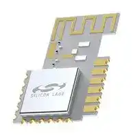


BGM210LA22JNF2
BLUETOOTH MOD, V5.1, -40 TO 105 DEG C
- Manufacturer: SILICON LABS
- Product type: Bluetooth Modules & Adaptors
- SVHC: To Be Advised
- Product Range: Blue Gecko BGM210L Series
- Bluetooth Class: -
- Bluetooth Version: Bluetooth 5.1
- Supply Voltage Range: 1.8 V to 3.8 V
- Receiver Sensitivity Rx: -93.9 dBm
- Operating Temperature Range: -40 °C to 105 °C
| Delivery and price | |
|---|---|
| Units per pack | 100 |
| Price | 4.05 € |
| Current stock | 10+ |
| Lead time | 30 days |
## **BGM210L Blue Gecko Bluetooth[®] Lighting Module Data Sheet**

## The BGM210L is a module designed and built to meet the performance, security, and reliability requirements of line-powered, smart LED lighting products.

Based on the EFR32BG21 Blue Gecko SoC, it enables Bluetooth 5.1 and Bluetooth Mesh connectivity delivering best-in-class RF performance, CA Title 20 energy consumption compliance, future-proof capability for feature and OTA firmware updates, enhanced security, and a form factor and temperature rating suited for enclosed operation in lightbulb housings.

## **KEY FEATURES**

- Bluetooth 5.1 and Bluetooth Mesh connectivity

- PCB Trace antenna

- +12.5 dBm Max TX power

- -97 dBm Bluetooth RX sensitivity @ 1 Mbps

- 32-bit ARM Cortex-M33 core at 38.4 MHz

The BGM210L is a complete solution that comes with fully-upgradeable, robust software stacks, world-wide regulatory certifications, advanced development and debugging tools, and support that will simplify and minimize the development cycle of your product helping to accelerate its time-to-market.

The BGM210L is targeted for key applications that include:

- Smart LED lightbulbs

   - 1024/96 kB of flash/RAM memory

   - Enhanced security features

   - Optimal set of MCU peripherals

   - 12 GPIO pins

   - -40 to (105 or 125)°C

   - 15.5 mm x 22.5 mm (custom form factor)

- Connected lighting

**==> picture [482 x 242] intentionally omitted <==**

**----- Start of picture text -----**<br>
Core / Memory Crystal Clock Management Energy  Security<br>Management<br>38.4  HF Crystal  HF Fast Startup Crypto<br>ARM Cortex [TM]  M33 processor MHz Oscillator RC Oscillator RC Oscillator Voltage  Acceleration<br>with DSP extensions, Flash Program  Regulator<br>FPU and TrustZone Memory EM23 HF RC  Secure Debug<br>Oscillator Brown-Out Detector True Random<br>Number Generator<br>ETM Debug Interface RAM Memory ControllerLDMA  LF Crystal Oscillator Ultra LF RC Oscillator RC OscillatorLF Power-On Reset Security Core<br>32-bit bus<br>Peripheral Reflex System<br>Antenna Radio Transceiver Serial  I/O Ports Timers and Triggers Analog I/F<br>Interfaces<br>PCB Trace<br>Antenna RF Frontend I DEMOD USART InterruptsExternal  Timer/Counter Protocol Timer ADC<br>LNA<br>Matching Q PGA IFADC I [2] C Purpose I/OGeneral  Low Energy Timer Watchdog Timer ComparatorAnalog<br>PA<br>AGC Pin Reset Capture CounterReal Time<br>PA Frequency<br>Synth<br>MOD Pin Wakeup Back-Up Real Time Counter<br>Lowest power mode with peripheral operational:<br>EM0—Active EM1—Sleep EM2—Deep Sleep EM3—Stop EM4—Shutoff<br>FRC BUFC<br>CRC RAC<br>**----- End of picture text -----**<br>


**silabs.com** | Building a more connected world.

Rev. 0.5.1

BGM210L Blue Gecko Bluetooth[®] Lighting Module Data Sheet Features

## **1.  Features**

- **Supported Protocols**

   - Bluetooth 5.1

      - AoA/AoD

   - Bluetooth Mesh

- **Wireless System-on-Chip**

   - 2.4 GHz radio

   - TX power up to +12.5 dBm

   - 32-bit ARM Cortex[®] -M33 with DSP instruction and floatingpoint unit for efficient signal processing

   - 1024 kB flash program memory

   - 96 kB RAM data memory

   - Embedded Trace Macrocell (ETM) for advanced debugging

- **Receiver Performance**

   - -104.4 dBm sensitivity (0.1% BER) at 125 kbps GFSK

   - -100.1 dBm sensitivity (0.1% BER) at 500 kbps GFSK

   - -97 dBm sensitivity (0.1% BER) at 1 Mbps GFSK

   - -93.9 dBm sensitivity (0.1% BER) at 2 Mbps GFSK

- **Current Consumption**

   - 9.3 mA RX current at 1 Mbps GFSK

   - 70 mA TX current at +12.5 dBm output power

   - 50.9 µA/MHz in Active Mode (EM0)

   - 5.1 μA EM2 DeepSleep current (RTCC running from LFXO, Bluetooth Stack not running)

   - 8.5 μA EM2 DeepSleep current (RTCC running from LFXO, Bluetooth Stack running)

- **Regulatory Certifications**

   - CE

   - ISED

   - FCC

   - Australia

   - Dominican Republic

   - **Operating Range**

      - 1.8 to 3.8 V

      - -40 to +105 °C or -40 to +125 °C

   - **Dimensions**

      - 15.5 mm x 22.5 mm (custom form factor)

   - **Security**

      - Secure Boot with Root of Trust and Secure Loader (RTSL) **[1]**

      - Hardware Cryptographic Acceleration with DPA countermeasures **[1]** for AES128/256, SHA-1, SHA-2 (up to 256-bit), ECC (up to 256-bit), ECDSA, and ECDH

      - True Random Number Generator (TRNG) compliant with NIST SP800-90 and AIS-31

      - ARM[®] TrustZone[®]

      - Secure Debug Interface lock/unlock

   - **MCU Peripherals**

      - 12-bit 1 Msps SAR Analog to Digital Converter (ADC)

      - 2 × Analog Comparator (ACMP)

      - 12 General Purpose I/O pins with output state retention and asynchronous interrupts

      - 8 Channel DMA Controller

      - 12 Channel Peripheral Reflex System (PRS)

      - 2 × 16-bit Timer/Counter (3 Compare/Capture/PWM channels)

      - 1 × 32-bit Timer/Counter (3 Compare/Capture/PWM channels)

      - 32-bit Real Time Counter

      - 24-bit Low Energy Timer for waveform generation

      - 2 × Watchdog Timer

      - 3 × Universal Synchronous/Asynchronous Receiver/Transmitter (UART/SPI/SmartCard (ISO 7816)/IrDA/I[2] S)

      - 2 × I[2] C interface with SMBus support

- Hong Kong

- Israel

- Jordan

- Kuwait

- Serbia

- Singapore

1. With Secure Element (SE) firmware v1.1.2 or newer

**silabs.com** | Building a more connected world.

Rev. 0.5.1  |  2

BGM210L Blue Gecko Bluetooth[®] Lighting Module Data Sheet Ordering Information

## **2.  Ordering Information**

**Table 2.1.  Ordering Information**

|**Ordering Code**|**Protocol Stack**|**Max TX**<br>**Power**|**Freq**<br>**Band**|**Antenna**|**Flash**<br>**(kB)**|**RAM**<br>**(kB)**|**GPIO**|**Temp Range**|**Packaging**|
|---|---|---|---|---|---|---|---|---|---|
|BGM210LA22JIF2|• Bluetooth 5.1|12.5 dBm|2.4 GHz|Inverted-F<br>PCB Trace|1024|96|12|-40 to 125 °C|Cut Tape|
|BGM210LA22JIF2R|• Bluetooth 5.1|12.5 dBm|2.4 GHz|Inverted-F<br>PCB Trace|1024|96|12|-40 to 125 °C|Reel|
|BGM210LA22JNF2|• Bluetooth 5.1|12.5 dBm|2.4 GHz|Inverted-F<br>PCB Trace|1024|96|12|-40 to 105 °C|Cut Tape|
|BGM210LA22JNF2R|• Bluetooth 5.1|12.5 dBm|2.4 GHz|Inverted-F<br>PCB Trace|1024|96|12|-40 to 105 °C|Reel|


End-product manufacturers must verify that the module is configured to meet regulatory limits for each region in accordance with the formal certification test reports.

Devices are pre-programmed with BGAPI UART DFU bootloader.

SLWRB4309B radio board is available for BGM210L evaluation and development.

**silabs.com** | Building a more connected world.

Rev. 0.5.1  |  3

## **Table of Contents**

|**1.**|**Features .**<br>**.**<br>**.**<br>**.**<br>**.**<br>**.**<br>**.**<br>**.**<br>**.**|**.**|**.**|**.**|**.**|**.**|**.**|**.**|**.**|**.**|**.**|**.**|**.**|**.**|**.**|**.**|**.**|**.**|**.**|**.**|**.**|**.**|**.**|**.**|**. 2**|
|---|---|---|---|---|---|---|---|---|---|---|---|---|---|---|---|---|---|---|---|---|---|---|---|---|---|
|**2.**|**Ordering Information**<br>**.**<br>**.**<br>**.**<br>**.**|**.**|**.**|**.**|**.**|**.**|**.**|**.**|**.**|**.**|**.**|**.**|**.**|**.**|**.**|**.**|**.**|**.**|**.**|**.**|**.**|**.**|**.**|**.**|**. 3**|
|**3.**|**System Overview .**<br>**.**<br>**.**<br>**.**<br>**.**<br>**.**|**.**|**.**|**.**|**.**|**.**|**.**|**.**|**.**|**.**|**.**|**.**|**.**|**.**|**.**|**.**|**.**|**.**|**.**|**.**|**.**|**.**|**.**|**.**|**. 6**|
||3.1  Block Diagram .<br>.<br>.<br>.<br>.<br>.|.|.|.|.|.|.|.|.|.|.|.|.|.|.|.|.|.|.|.|.|.|.|.|. 6|
||3.2  EFR32BG21 SoC .<br>.<br>.<br>.<br>.|.|.|.|.|.|.|.|.|.|.|.|.|.|.|.|.|.|.|.|.|.|.|.|. 6|
||3.3  Antenna .<br>.<br>.<br>.<br>.<br>.<br>.<br>.|.|.|.|.|.|.|.|.|.|.|.|.|.|.|.|.|.|.|.|.|.|.|.|. 6|
||3.4  Power Supply<br>.<br>.<br>.<br>.<br>.<br>.|.|.|.|.|.|.|.|.|.|.|.|.|.|.|.|.|.|.|.|.|.|.|.|. 6|
|**4.**|**Electrical Specifications .**<br>**.**<br>**.**|**.**|**.**|**.**|**.**|**.**|**.**|**.**|**.**|**.**|**.**|**.**|**.**|**.**|**.**|**.**|**.**|**.**|**.**|**.**|**.**|**.**|**.**|**.**|**. 7**|
||4.1  Electrical Characteristics<br>.<br>.|.|.|.|.|.|.|.|.|.|.|.|.|.|.|.|.|.|.|.|.|.|.|.|. 7|
||4.1.1  Absolute Maximum Ratings|.|.|.|.|.|.|.|.|.|.|.|.|.|.|.|.|.|.|.|.|.|.|.|. 7|
||4.1.2  General Operating Conditions||.|.|.|.|.|.|.|.|.|.|.|.|.|.|.|.|.|.|.|.|.|.|. 8|
||4.1.3  MCU Current Consumption at 3.0V.||||.|.|.|.|.|.|.|.|.|.|.|.|.|.|.|.|.|.|.|.|. 9|
||4.1.4  Radio Current Consumption|at|3.0V||.|.|.|.|.|.|.|.|.|.|.|.|.|.|.|.|.|.|.|.|.10|
||4.1.5  RF Transmitter General Characteristics|||||for|the 2.4 GHz Band.|||||||.|.|.|.|.|.|.|.|.|.|.|.11|
||4.1.6  RF Receiver General Characteristics||||for the 2.4||||GHz Band||||.|.|.|.|.|.|.|.|.|.|.|.|.11|
||4.1.7  RF Receiver Characteristics for Bluetooth Low Energy||||||||||at|1 Mbps|||.|.|.|.|.|.|.|.|.|.|.12|
||4.1.8  RF Receiver Characteristics for Bluetooth Low Energy||||||||||at|2 Mbps|||.|.|.|.|.|.|.|.|.|.|.13|
||4.1.9  RF Receiver Characteristics for Bluetooth Low Energy||||||||||at|500 kbps|||.|.|.|.|.|.|.|.|.|.|.14|
||4.1.10  RF Receiver Characteristics for Bluetooth Low||||||||Energy at 125|||||kbps||.|.|.|.|.|.|.|.|.|.15|
||4.1.11  High-Frequency Crystal .|.|.|.|.|.|.|.|.|.|.|.|.|.|.|.|.|.|.|.|.|.|.|.|.16|
||4.1.12  GPIO Pins<br>.<br>.<br>.<br>.<br>.|.|.|.|.|.|.|.|.|.|.|.|.|.|.|.|.|.|.|.|.|.|.|.|.16|
||4.1.13  Microcontroller Peripherals .||.|.|.|.|.|.|.|.|.|.|.|.|.|.|.|.|.|.|.|.|.|.|.17|
||4.2  Typical Performance Curves<br>.|.|.|.|.|.|.|.|.|.|.|.|.|.|.|.|.|.|.|.|.|.|.|.|.17|
||4.2.1  Antenna Radiation and Efficiency|||.|.|.|.|.|.|.|.|.|.|.|.|.|.|.|.|.|.|.|.|.|.18|
|**5.**|**Reference Diagrams.**<br>**.**<br>**.**<br>**.**<br>**.**|**.**|**.**|**.**|**.**|**.**|**.**|**.**|**.**|**.**|**.**|**.**|**.**|**.**|**.**|**.**|**.**|**.**|**.**|**.**|**.**|**.**|**.**|**.**|**19**|
|**6.**|**Pin Definitions .**<br>**.**<br>**.**<br>**.**<br>**.**<br>**.**<br>**.**|**.**|**.**|**.**|**.**|**.**|**.**|**.**|**.**|**.**|**.**|**.**|**.**|**.**|**.**|**.**|**.**|**.**|**.**|**.**|**.**|**.**|**.**|**.**|**20**|
||6.1  Module Pinout .<br>.<br>.<br>.<br>.<br>.|.|.|.|.|.|.|.|.|.|.|.|.|.|.|.|.|.|.|.|.|.|.|.|.20|
||6.2  Alternate Pin Functions .<br>.<br>.|.|.|.|.|.|.|.|.|.|.|.|.|.|.|.|.|.|.|.|.|.|.|.|.21|
||6.3  Analog Peripheral Connectivity|.|.|.|.|.|.|.|.|.|.|.|.|.|.|.|.|.|.|.|.|.|.|.|.21|
||6.4  Digital Peripheral Connectivity .|.|.|.|.|.|.|.|.|.|.|.|.|.|.|.|.|.|.|.|.|.|.|.|.22|
|**7.**|**Design Guidelines**<br>**.**<br>**.**<br>**.**<br>**.**|**.**|**.**|**.**|**.**|**.**|**.**|**.**|**.**|**.**|**.**|**.**|**.**|**.**|**.**|**.**|**.**|**.**|**.**|**.**|**.**|**.**|**.**|**.**|**. 25**|
||7.1  Module Placement.<br>.<br>.<br>.<br>.|.|.|.|.|.|.|.|.|.|.|.|.|.|.|.|.|.|.|.|.|.|.|.|.25|
||7.2  Antenna .<br>.<br>.<br>.<br>.<br>.<br>.<br>.|.|.|.|.|.|.|.|.|.|.|.|.|.|.|.|.|.|.|.|.|.|.|.|.26|
|**8.**|**Package Specifications**<br>**.**<br>**.**|**.**|**.**|**.**|**.**|**.**|**.**|**.**|**.**|**.**|**.**|**.**|**.**|**.**|**.**|**.**|**.**|**.**|**.**|**.**|**.**|**.**|**.**|**.**|**.27**|
||8.1  Dimensions .<br>.<br>.<br>.<br>.<br>.<br>.|.|.|.|.|.|.|.|.|.|.|.|.|.|.|.|.|.|.|.|.|.|.|.|.27|
||8.2  PCB Land Pattern .<br>.<br>.<br>.<br>.|.|.|.|.|.|.|.|.|.|.|.|.|.|.|.|.|.|.|.|.|.|.|.|.28|
||8.3  Marking<br>.<br>.<br>.<br>.<br>.<br>.<br>.<br>.|.|.|.|.|.|.|.|.|.|.|.|.|.|.|.|.|.|.|.|.|.|.|.|.29|


**silabs.com** | Building a more connected world.

Rev. 0.5.1 |  4

|**9.  Soldering Recommendations**|**9.  Soldering Recommendations**|**9.  Soldering Recommendations**|**9.  Soldering Recommendations**|**9.  Soldering Recommendations**|**9.  Soldering Recommendations**||**.**||**.**||**.**||**.**||**.**||**.**||**.**||**.**||**.**||**.**||**.**||**.**||**.**||**.**||**.**||**.**||**.**||**.**||**.**||**.**||**.**||**.**||**.**||**. 30**|
|---|---|---|---|---|---|---|---|---|---|---|---|---|---|---|---|---|---|---|---|---|---|---|---|---|---|---|---|---|---|---|---|---|---|---|---|---|---|---|---|---|---|---|---|---|---|---|---|---|---|---|---|---|---|
|**10.  Tape and Reel**||**.**|**.**|**.**|**.**|**.**||**.**||**.**||**.**||**.**||**.**||**.**||**.**||**.**||**.**||**.**||**.**||**.**||**.**||**.**||**.**||**.**||**.**||**.**||**.**||**.**||**.**||**.**||**.**|**.31**|
|**11.  Certifications .**|**.**|**.**|**.**|**.**|**.**|**.**||**.**||**.**||**.**||**.**||**.**||**.**||**.**||**.**||**.**||**.**||**.**||**.**||**.**||**.**||**.**||**.**||**.**||**.**||**.**||**.**||**.**||**.**||**.**|**32**|
|11.1  CE<br>.<br>.<br>.|.|.|.|.|.|.||.||.||.||.||.||.||.||.||.||.||.||.||.||.||.||.||.||.||.||.||.||.||.|.32|
|11.2  FCC .<br>.<br>.|.|.|.|.|.|.||.||.||.||.||.||.||.||.||.||.||.||.||.||.||.||.||.||.||.||.||.||.||.|.32|
|11.3  ISED Canada|.|.|.|.|.|.||.||.||.||.||.||.||.||.||.||.||.||.||.||.||.||.||.||.||.||.||.||.||.|.33|
|11.4  Australia<br>.|.|.|.|.|.|.||.||.||.||.||.||.||.||.||.||.||.||.||.||.||.||.||.||.||.||.||.||.||.|.34|
|11.5  Dominican Republic.||||.|.|.||.||.||.||.||.||.||.||.||.||.||.||.||.||.||.||.||.||.||.||.||.||.||.|.34|
|11.6  Hong Kong .|.|.|.|.|.|.||.||.||.||.||.||.||.||.||.||.||.||.||.||.||.||.||.||.||.||.||.||.||.|.35|
|11.7  Israel.<br>.<br>.|.|.|.|.|.|.||.||.||.||.||.||.||.||.||.||.||.||.||.||.||.||.||.||.||.||.||.||.||.|.35|
|11.8  Jordan<br>.<br>.|.|.|.|.|.|.||.||.||.||.||.||.||.||.||.||.||.||.||.||.||.||.||.||.||.||.||.||.||.|.35|
|11.9  Kuwait<br>.<br>.|.|.|.|.|.|.||.||.||.||.||.||.||.||.||.||.||.||.||.||.||.||.||.||.||.||.||.||.||.|.35|
|11.10  Serbia .<br>.|.|.|.|.|.|.||.||.||.||.||.||.||.||.||.||.||.||.||.||.||.||.||.||.||.||.||.||.||.|.35|
|11.11  Singapore.|.|.|.|.|.|.||.||.||.||.||.||.||.||.||.||.||.||.||.||.||.||.||.||.||.||.||.||.||.|.35|
|**12.  Revision History.**||**.**|**.**|**.**|**.**|**.**||**.**||**.**||**.**||**.**||**.**||**.**||**.**||**.**||**.**||**.**||**.**||**.**||**.**||**.**||**.**||**.**||**.**||**.**||**.**||**.**||**.**||**.**||**.**|**36**|


**silabs.com** | Building a more connected world.

Rev. 0.5.1 |  5

BGM210L Blue Gecko Bluetooth[®] Lighting Module Data Sheet System Overview

## **3.  System Overview**

## **3.1  Block Diagram**

The BGM210L module is a highly-integrated, high-performance system with all the hardware components needed to enable 2.4 GHz wireless connectivity and support robust networking capabilities via multiple protocols.

Built around the EFR32BG21 Wireless Gecko SoC, the BGM210L includes a built-in PCB trace antenna, an RF matching network (optimized for transmit power efficiency), supply decoupling and filtering components, a 38.4 MHz reference crystal, and an RF shield. A general block diagram of the module is shown below.

**==> picture [254 x 174] intentionally omitted <==**

**----- Start of picture text -----**<br>
Supply Decoupling LPF VDD<br>DEC<br>Antenna<br>RF Match Silicon Labs (up to 12) GP IO<br>EFR32BG21<br>HF XTAL GND<br>RF SHIELD<br>**----- End of picture text -----**<br>


**Figure 3.1.  BGM210L Block Diagram**

## **3.2  EFR32BG21 SoC**

The EFR32BG21 SoC features a 32-bit ARM Cortex M33 core, a 2.4 GHz high-performance radio, 1 MB of Flash memory, a dedicated core for security, a rich set of MCU peripherals, and various clock management and serial interfacing options. Consult the EFR32xG21 Wireless Gecko Reference Manual and the EFR32BG21 Data Sheet for details (See EFR32BG21A020F1024IM32).

## **3.3  Antenna**

BGM210L modules include a built-in PCB trace antenna with the characteristics seen below. The design of the antenna is optimized to operate the module mounted on an application board with a thickness of 0.8 mm.

**Table 3.1.  Antenna Efficiency and Peak Gain**

|**Parameter**|**With optimal layout **|**Note**|
|---|---|---|
|Efficiency|-2 to -2.5 dB|Antenna efficiency, gain and radiation pattern are highly depend-<br>ent on the application PCB layout and mechanical design. Refer<br>to7. Design Guidelinesfor PCB layout and antenna integration<br>guidelines for optimal performance.|
|Peak gain|0.5 dBi||


## **3.4  Power Supply**

The BGM210L requires a single nominal supply level of 3.0 V. All the necessary decoupling and filtering components are included in the module. The module can tolerate supply voltage noise of up to 700 mVpp.

The supply voltage is filtered internally in the module with a 100 kHz low-pass filter to guarantee operation across the full supply range of 1.8 to 3.8 V. Additional external filtering is neither required nor recommended as it may cause voltage drops below the minimum level tolerable by the SoC (1.71 V) during transmit bursts.

For typical use cases, the decouple pin (DEC) should be left disconnected.

**silabs.com** | Building a more connected world.

Rev. 0.5.1  |  6

BGM210L Blue Gecko Bluetooth[®] Lighting Module Data Sheet Electrical Specifications

## **4.  Electrical Specifications**

## **4.1  Electrical Characteristics**

All electrical parameters in all tables are specified under the following conditions, unless stated otherwise:

- Typical values are based on TA=25 °C and VDD = 3.0 V, by production test and/or technology characterization.

- Radio performance numbers are measured in conducted mode, based on Silicon Laboratories reference designs using output power-specific external RF impedance-matching networks for interfacing to a 50 Ω antenna.

- Minimum and maximum values represent the worst conditions across supply voltage, process variation, and operating temperature, unless stated otherwise.

## **4.1.1  Absolute Maximum Ratings**

Stresses above those listed below may cause permanent damage to the device. This is a stress rating only and functional operation of the devices at those or any other conditions above those indicated in the operation listings of this specification is not implied. Exposure to maximum rating conditions for extended periods may affect device reliability. For more information on the available quality and reliability data, see the Quality and Reliability Monitor Report at http://www.silabs.com/support/quality/pages/default.aspx.

**Table 4.1.  Absolute Maximum Ratings**

|**Parameter**|**Symbol**|**Test Condition**|**Min**|**Typ**|**Max**|**Unit**|
|---|---|---|---|---|---|---|
|Storage temperature range|TSTG||-50|—|+150|°C|
|Voltage on VDD supply pin|VDDMAX||-0.3|—|3.8|V|
|Voltage ramp rate on VDD<br>supply pin|VDDRAMPMAX||—|—|1.0|V / µs|
|DC voltage on any GPIO pin|VDIGPIN||-0.3|—|VDD+ 0.3|V|
|Total current into VDD pin|IVDDMAX|Source|—|—|200|mA|
|Total current into GND pin|IGNDMAX|Sink|—|—|200|mA|
|Current per I/O pin|IIOMAX|Sink|—|—|50|mA|
|||Source|—|—|50|mA|
|Current for all I/O pins|IIOALLMAX|Sink|—|—|200|mA|
|||Source|—|—|200|mA|
|Junction temperature|TJMAX||—|—|+125|°C|


**silabs.com** | Building a more connected world.

Rev. 0.5.1  |  7

BGM210L Blue Gecko Bluetooth[®] Lighting Module Data Sheet Electrical Specifications

## **4.1.2  General Operating Conditions**

This table specifies the general operating temperature range and supply voltage range for all supplies. The minimum and maximum values of all other tables are specifed over this operating range, unless otherwise noted.

**Table 4.2.  General Operating Conditions**

|**Parameter**|**Symbol**|**Test Condition**|**Min**|**Typ**|**Max**|**Unit**|
|---|---|---|---|---|---|---|
|Operating ambient tempera-<br>ture range|TA|-N temperature grade|-40|—|+105|°C|
|||-I temperature grade|-40|—|+125|° C|
|VDD Supply Voltage|VDD||1.8|3.0|3.8|V|
|HCLK and Core frequency|fHCLK|MODE = WS1, RAMWSEN = 11|—|—|80|MHz|
|||MODE = WS1, RAMWSEN = 01|—|—|50|MHz|
|||MODE = WS0, RAMWSEN = 01|—|—|39|MHz|
|PCLK frequency|fPCLK||—|—|50|MHz|
|EM01 Group A clock fre-<br>quency|fEM01GRPACLK||—|—|80|MHz|
|HCLK Radio frequency|fHCLKRADIO||—|38.4|—|MHz|
|**Note:**<br>1. Flash wait states are set by the MODE field in the MSC_READCTRL register. RAM wait states are enabled by setting the RAMW-<br>SEN bit in the SYSYCFG_DMEM0RAMCTRL register.|||||||


**silabs.com** | Building a more connected world.

Rev. 0.5.1  |  8

BGM210L Blue Gecko Bluetooth[®] Lighting Module Data Sheet Electrical Specifications

## **4.1.3  MCU Current Consumption at 3.0V**

Unless otherwise indicated, typical conditions are: VDD = 3.0 V. TA = 25 °C. Minimum and maximum values in this table represent the worst conditions across process variation at TA = 25 °C.

**Table 4.3.  MCU Current Consumption at 3.0V**

|**Parameter**|**Symbol**|**Test Condition**|**Min**|**Typ**|**Max**|**Unit**|
|---|---|---|---|---|---|---|
|Current consumption in EM0<br>mode with all peripherals dis-<br>abled1|IACTIVE|80 MHz HFRCO, CPU running<br>Prime from flash|—|50.9|—|µA/MHz|
|||80 MHz HFRCO, CPU running<br>while loop from flash|—|45.6|55.5|µA/MHz|
|||80 MHz HFRCO, CPU running<br>CoreMark loop from flash|—|59.8|—|µA/MHz|
|||38.4 MHz crystal, CPU running<br>while loop from flash|—|63.8|—|µA/MHz|
|Current consumption in EM1<br>mode with all peripherals dis-<br>abled1|IEM1|80 MHz HFRCO|—|28.7|37.6|µA/MHz|
|||38.4 MHz crystal|—|46.9|—|µA/MHz|
|Current consumption in EM2<br>mode|IEM2|Full RAM retention and RTC run-<br>ning from LFXO (Bluetooth Stack<br>not running)|—|5.1|—|µA|
|||Full RAM retention, RTCC run-<br>ning, and Bluetooth Stack running<br>from LFXO|—|8.5|—|µA|
|||1 bank (16 kB) RAM retention and<br>RTC running from LFRCO|—|4.5|10.5|µA|
|Current consumption in EM3<br>mode|IEM3|Full RAM retention and RTC run-<br>ning from ULFRCO|—|4.8|11.4|µA|
|||1 bank (16 kB) RAM retention and<br>RTC running from ULFRCO|—|4.3|—|µA|
|Current consumption in EM4<br>mode|IEM4|No BURTC, no LF oscillator|—|0.21|0.5|µA|
|Current consumption during<br>reset|IRST|Hard pin reset held|—|146|—|µA|
|Current consumption per re-<br>tained 16kB RAM bank in<br>EM2|IRAM||—|0.10|—|µA|
|**Note:**<br>1. The typical EM0/EM1 current measurement includes some current consumed by the security core for periodical housekeeping<br>purposes. This does not include current consumed by user-triggered security operations, such as cryptographic calculations.|||||||


**silabs.com** | Building a more connected world.

Rev. 0.5.1  |  9

BGM210L Blue Gecko Bluetooth[®] Lighting Module Data Sheet Electrical Specifications

## **4.1.4  Radio Current Consumption at 3.0V**

RF current consumption measured with MCU in EM1, HCLK = 38.4 MHz, and all MCU peripherals disabled. Unless otherwise indicated, typical conditions are: VDD = 3.0V. TA = 25 °C. Minimum and maximum values in this table represent the worst conditions across process variation at TA = 25 °C.

**Table 4.4.  Radio Current Consumption at 3.0V**

|**Parameter**|**Symbol**|**Test Condition**|**Min**|**Typ**|**Max**|**Unit**|
|---|---|---|---|---|---|---|
|Current consumption in re-<br>ceive mode, active packet<br>reception|IRX_ACTIVE|125 kbit/s, 2GFSK, f = 2.4 GHz,<br>Bluetooth stack running|—|9.3|—|mA|
|||500 kbit/s, 2GFSK, f = 2.4 GHz,<br>Bluetooth stack running|—|9.3|—|mA|
|||1 Mbit/s, 2GFSK, f = 2.4 GHz,<br>Bluetooth stack running|—|9.3|—|mA|
|||2 Mbit/s, 2GFSK, f = 2.4 GHz,<br>Bluetooth stack running|—|9.9|—|mA|
|Current consumption in re-<br>ceive mode, Stack running|IRX_LISTEN|125 kbit/s, 2GFSK, f = 2.4 GHz,<br>Bluetooth stack running|—|9.1|—|mA|
|||500 kbit/s, 2GFSK, f = 2.4 GHz,<br>Bluetooth stack running|—|9.1|—|mA|
|||1 Mbit/s, 2GFSK, f = 2.4 GHz,<br>Bluetooth stack running|—|9.1|—|mA|
|||2 Mbit/s, 2GFSK, f = 2.4 GHz,<br>Bluetooh stack running|—|9.8|—|mA|
|Current consumption in<br>transmit mode|ITX|f = 2.4 GHz, CW, 12.5 dBm output<br>power, VDD = 3.3 V|—|70|—|mA|


**silabs.com** | Building a more connected world.

Rev. 0.5.1  |  10

BGM210L Blue Gecko Bluetooth[®] Lighting Module Data Sheet Electrical Specifications

## **4.1.5  RF Transmitter General Characteristics for the 2.4 GHz Band**

Unless otherwise indicated, typical conditions are: TA = 25 °C, VDD = 3.0V. RF center frequency 2.45 GHz.[1]

**Table 4.5.  RF Transmitter General Characteristics for the 2.4 GHz Band**

|**Parameter**|**Symbol**|**Test Condition**|**Min**|**Typ**|**Max**|**Unit**|
|---|---|---|---|---|---|---|
|RF tuning frequency range|FRANGE||2400|—|2483.5|MHz|
|Maximum TX power23|POUTMAX|12 dBm PA, VDD = 3.3 V|—|12.5|—|dBm|
|Minimum active TX Power|POUTMIN|12 dBm PA, VDD = 3.3 V|—|TBD|—|dBm|
|Output power variation vs<br>VDD supply voltage varia-<br>tion, frequency = 2450MHz|POUTVAR_V|12 dBm PA Pout= POUTMAXout-<br>put power with VDD voltage swept<br>from 3.8V to 3.0V.|—|+/- 0.5|—|dB|
|||12 dBm PA Pout= POUTMAXout-<br>put power with VDD voltage swept<br>from 3.8V to 1.8V|—|+0.5/-4.5|—|dB|
|Output power variation vs RF<br>frequency|POUTVAR_F|12 dBm PA, POUTMAX, VDD =<br>3.3 V.|—|+/- 0.1|—|dB|
|**Note:**<br>1. For regulatory compliance please refer to the official certification test reports<br>2. Supported transmit power levels are determined by the ordering part number (OPN). Transmit power ratings for all devices cov-<br>ered in this data sheet can be found in the TX Power column of the Ordering Information Table.<br>3. The maximum TXP to comply with ETSI PSD and EIRP limits depend on antenna gain which in turn depend on the end product<br>mechanical design. In optimal conditions the module is compliant to the ETSI PSD and EIRP limits at maximum TXP of 8.2 dBm.<br>End product manufacturer must ensure compliance to the limits for CE marking of the end product.|||||||


## **4.1.6  RF Receiver General Characteristics for the 2.4 GHz Band**

Unless otherwise indicated, typical conditions are: TA = 25 °C, VDD = 3.0V. RF center frequency 2.45 GHz.

**Table 4.6.  RF Receiver General Characteristics for the 2.4 GHz Band**

|**Parameter**|**Symbol**|**Test Condition**|**Min**|**Typ**|**Max**|**Unit**|
|---|---|---|---|---|---|---|
|RF tuning frequency range|FRANGE||2400|—|2483.5|MHz|


**silabs.com** | Building a more connected world.

Rev. 0.5.1  |  11

BGM210L Blue Gecko Bluetooth[®] Lighting Module Data Sheet Electrical Specifications

## **4.1.7  RF Receiver Characteristics for Bluetooth Low Energy at 1 Mbps**

Unless otherwise indicated, typical conditions are: TA = 25 °C, VDD = 3.0V. RF center frequency 2.45 GHz.

**Table 4.7.  RF Receiver Characteristics for Bluetooth Low Energy at 1 Mbps**

|**Parameter**|**Symbol**|**Test Condition**|**Min**|**Typ**|**Max**|**Unit**|
|---|---|---|---|---|---|---|
|Max usable receiver input<br>level|SAT|Signal is reference signal, packet<br>length is 37 bytes1|—|10|—|dBm|
|Sensitivity|SENS|Signal is reference signal, 37 byte<br>payload1|—|-97|—|dBm|
|||With non-ideal signals2 1|—|-96.5|—|dBm|
|Signal to co-channel interfer-<br>er|C/ICC|(see notes)1 3|—|+6.6|—|dB|
|N ± 1 Adjacent channel se-<br>lectivity|C/I1|Interferer is reference signal at +1<br>MHz offset1 4 3 5|—|-8.3|—|dB|
|||Interferer is reference signal at -1<br>MHz offset1 4 3 5|—|-8.7|—|dB|
|N ± 2 Alternate channel se-<br>lectivity|C/I2|Interferer is reference signal at +2<br>MHz offset1 4 3 5|—|-42.1|—|dB|
|||Interferer is reference signal at -2<br>MHz offset1 4 3 5|—|-48.9|—|dB|
|N ± 3 Alternate channel se-<br>lectivity|C/I3|Interferer is reference signal at +3<br>MHz offset1 4 3 5|—|-42.4|—|dB|
|||Interferer is reference signal at -3<br>MHz offset1 4 3 5|—|-54.8|—|dB|
|Selectivity to image frequen-<br>cy|C/IIM|Interferer is reference signal at im-<br>age frequency with 1 MHz preci-<br>sion1 5|—|-42.1|—|dB|
|Selectivity to image frequen-<br>cy ± 1 MHz|C/IIM_1|Interferer is reference signal at im-<br>age frequency +1 MHz with 1<br>MHz precision1 5|—|-42.4|—|dB|
|||Interferer is reference signal at im-<br>age frequency -1 MHz with 1 MHz<br>precision1 5|—|-8.3|—|dB|
|Intermodulation performance|IM|n = 36|—|-23|—|dBm|
|**Note:**<br>1. 0.1% Bit Error Rate.<br>2. With non-ideal signals as specified in Bluetooth Test Specification RF-PHY.TS.5.0.1 section 4.7.1<br>3. Desired signal -67 dBm.<br>4. Desired frequency 2402 MHz ≤ Fc ≤ 2480 MHz.<br>5. With allowed exceptions.<br>6. As specified in Bluetooth Core specification version 5.1, Vol 6, Part A, Section 4.4|||||||


**silabs.com** | Building a more connected world.

Rev. 0.5.1  |  12

BGM210L Blue Gecko Bluetooth[®] Lighting Module Data Sheet Electrical Specifications

## **4.1.8  RF Receiver Characteristics for Bluetooth Low Energy at 2 Mbps**

Unless otherwise indicated, typical conditions are: TA = 25 °C, VDD = 3.0V. RF center frequency 2.45 GHz.

**Table 4.8.  RF Receiver Characteristics for Bluetooth Low Energy at 2 Mbps**

|**Parameter**|**Symbol**|**Test Condition**|**Min**|**Typ**|**Max**|**Unit**|
|---|---|---|---|---|---|---|
|Max usable receiver input<br>level|SAT|Signal is reference signal, packet<br>length is 37 bytes1|—|10|—|dBm|
|Sensitivity|SENS|Signal is reference signal, 37 byte<br>payload1|—|-93.9|—|dBm|
|||With non-ideal signals2 1|—|-93.4|—|dBm|
|Signal to co-channel interfer-<br>er|C/ICC|(see notes)1 3|—|+6.0|—|dB|
|N ± 1 Adjacent channel se-<br>lectivity|C/I1|Interferer is reference signal at +2<br>MHz offset1 4 3 5|—|-8.0|—|dB|
|||Interferer is reference signal at -2<br>MHz offset1 4 3 5|—|-8.8|—|dB|
|N ± 2 Alternate channel se-<br>lectivity|C/I2|Interferer is reference signal at +4<br>MHz offset1 4 3 5|—|-42.2|—|dB|
|||Interferer is reference signal at -4<br>MHz offset1 4 3 5|—|-50.3|—|dB|
|N ± 3 Alternate channel se-<br>lectivity|C/I3|Interferer is reference signal at +6<br>MHz offset1 4 3 5|—|-54.4|—|dB|
|||Interferer is reference signal at -6<br>MHz offset1 4 3 5|—|-55.4|—|dB|
|Selectivity to image frequen-<br>cy|C/IIM|Interferer is reference signal at im-<br>age frequency with 1 MHz preci-<br>sion1 5|—|-8.0|—|dB|
|Selectivity to image frequen-<br>cy ± 1 MHz|C/IIM_1|Interferer is reference signal at im-<br>age frequency +2 MHz with 1<br>MHz precision1 5|—|-42.2|—|dB|
|||Interferer is reference signal at im-<br>age frequency -2 MHz with 1 MHz<br>precision1 5|—|+6.0|—|dB|
|Intermodulation performance|IM|n = 36|—|-22.3|—|dBm|
|**Note:**<br>1. 0.1% Bit Error Rate.<br>2. With non-ideal signals as specified in Bluetooth Test Specification RF-PHY.TS.5.0.1 section 4.7.1<br>3. Desired signal -67 dBm.<br>4. Desired frequency 2402 MHz ≤ Fc ≤ 2480 MHz.<br>5. With allowed exceptions.<br>6. As specified in Bluetooth Core specification version 5.1, Vol 6, Part A, Section 4.4|||||||


**silabs.com** | Building a more connected world.

Rev. 0.5.1  |  13

BGM210L Blue Gecko Bluetooth[®] Lighting Module Data Sheet Electrical Specifications

## **4.1.9  RF Receiver Characteristics for Bluetooth Low Energy at 500 kbps**

Unless otherwise indicated, typical conditions are: TA = 25 °C, VDD = 3.0V. RF center frequency 2.45 GHz.

**Table 4.9.  RF Receiver Characteristics for Bluetooth Low Energy at 500 kbps**

|**Parameter**|**Symbol**|**Test Condition**|**Min**|**Typ**|**Max**|**Unit**|
|---|---|---|---|---|---|---|
|Max usable receiver input<br>level|SAT|Signal is reference signal, packet<br>length is 37 bytes1|—|10|—|dBm|
|Sensitivity|SENS|Signal is reference signal1|—|-100.1|—|dBm|
|||With non-ideal signals2 1|—|-99.5|—|dBm|
|Signal to co-channel interfer-<br>er|C/ICC|(see notes)1 3|—|+2.1|—|dB|
|N ± 1 Adjacent channel se-<br>lectivity|C/I1|Interferer is reference signal at +1<br>MHz offset1 4 3 5|—|-9.0|—|dB|
|||Interferer is reference signal at -1<br>MHz offset1 4 3 5|—|-9.5|—|dB|
|N ± 2 Alternate channel se-<br>lectivity|C/I2|Interferer is reference signal at +2<br>MHz offset1 4 3 5|—|-44.4|—|dB|
|||Interferer is reference signal at -2<br>MHz offset1 4 3 5|—|-51.9|—|dB|
|N ± 3 Alternate channel se-<br>lectivity|C/I3|Interferer is reference signal at +3<br>MHz offset1 4 3 5|—|-44.3|—|dB|
|||Interferer is reference signal at -3<br>MHz offset1 4 3 5|—|-58.3|—|dB|
|Selectivity to image frequen-<br>cy|C/IIM|Interferer is reference signal at im-<br>age frequency with 1 MHz preci-<br>sion1 5|—|-44.4|—|dB|
|Selectivity to image frequen-<br>cy ± 1 MHz|C/IIM_1|Interferer is reference signal at im-<br>age frequency +1 MHz with 1<br>MHz precision1 5|—|-44.3|—|dB|
|||Interferer is reference signal at im-<br>age frequency -1 MHz with 1 MHz<br>precision1 5|—|-9.0|—|dB|
|**Note:**<br>1. 0.1% Bit Error Rate.<br>2. With non-ideal signals as specified in Bluetooth Test Specification RF-PHY.TS.5.0.1 section 4.7.1<br>3. Desired signal -72 dBm.<br>4. Desired frequency 2402 MHz ≤ Fc ≤ 2480 MHz.<br>5. With allowed exceptions.|||||||


**silabs.com** | Building a more connected world.

Rev. 0.5.1  |  14

BGM210L Blue Gecko Bluetooth[®] Lighting Module Data Sheet Electrical Specifications

## **4.1.10  RF Receiver Characteristics for Bluetooth Low Energy at 125 kbps**

Unless otherwise indicated, typical conditions are: TA = 25 °C, VDD = 3.0V. RF center frequency 2.45 GHz.

**Table 4.10.  RF Receiver Characteristics for Bluetooth Low Energy at 125 kbps**

|**Parameter**|**Symbol**|**Test Condition**|**Min**|**Typ**|**Max**|**Unit**|
|---|---|---|---|---|---|---|
|Max usable receiver input<br>level|SAT|Signal is reference signal, packet<br>length is 37 bytes1|—|10|—|dBm|
|Sensitivity|SENS|Signal is reference signal1|—|-104.4|—|dBm|
|||With non-ideal signals2 1|—|-104.1|—|dBm|
|Signal to co-channel interfer-<br>er|C/ICC|(see notes)1 3|—|+0.8|—|dB|
|N ± 1 Adjacent channel se-<br>lectivity|C/I1|Interferer is reference signal at +1<br>MHz offset1 4 3 5|—|-13.1|—|dB|
|||Interferer is reference signal at -1<br>MHz offset1 4 3 5|—|-13.6|—|dB|
|N ± 2 Alternate channel se-<br>lectivity|C/I2|Interferer is reference signal at +2<br>MHz offset1 4 3 5|—|-49.5|—|dB|
|||Interferer is reference signal at -2<br>MHz offset1 4 3 5|—|-56.9|—|dB|
|N ± 3 Alternate channel se-<br>lectivity|C/I3|Interferer is reference signal at +3<br>MHz offset1 4 3 5|—|-47.0|—|dB|
|||Interferer is reference signal at -3<br>MHz offset1 4 3 5|—|-63.1|—|dB|
|Selectivity to image frequen-<br>cy|C/IIM|Interferer is reference signal at im-<br>age frequency with 1 MHz preci-<br>sion1 5|—|-49.5|—|dB|
|Selectivity to image frequen-<br>cy ± 1 MHz|C/IIM_1|Interferer is reference signal at im-<br>age frequency +1 MHz with 1<br>MHz precision1 5|—|-47.0|—|dB|
|||Interferer is reference signal at im-<br>age frequency -1 MHz with 1 MHz<br>precision1 5|—|-13.1|—|dB|
|**Note:**<br>1. 0.1% Bit Error Rate.<br>2. With non-ideal signals as specified in Bluetooth Test Specification RF-PHY.TS.5.0.1 section 4.7.1<br>3. Desired signal -79 dBm.<br>4. Desired frequency 2402 MHz ≤ Fc ≤ 2480 MHz.<br>5. With allowed exceptions.|||||||


**silabs.com** | Building a more connected world.

Rev. 0.5.1  |  15

BGM210L Blue Gecko Bluetooth[®] Lighting Module Data Sheet Electrical Specifications

## **4.1.11  High-Frequency Crystal**

**Table 4.11.  High-Frequency Crystal**

|**Parameter**|**Symbol**|**Test Condition**|**Min**|**Typ**|**Max**|**Unit**|
|---|---|---|---|---|---|---|
|Crystal frequency|fHFXTAL||—|38.4|—|MHz|
|Initial calibrated accuracy|ACCHFXTAL||-10|—|+10|ppm|
|Temperature drift|DRIFTHFXTAL|Across specified temperature<br>range|-30|—|+30|ppm|


## **4.1.12  GPIO Pins**

Unless otherwise indicated, typical conditions are: VDD = 3.0 V.

**Table 4.12.  GPIO Pins**

|**Parameter**|**Symbol**|**Test Condition**|**Min**|**Typ**|**Max**|**Unit**|
|---|---|---|---|---|---|---|
|Leakage current|ILEAK_IO|MODEx = DISABLED, VDD =<br>1.71V|—|1.9|—|nA|
|||MODEx = DISABLED, VDD = 3.0<br>V|—|2.5|—|nA|
|Input low voltage1|VIL|Any GPIO pin|—|—|0.3 * VDD|V|
|Input high voltage1|VIH|Any GPIO pin|0.7 * VDD|—|—|V|
|Output low voltage|VOL|Sinking 20mA, VDD = 3.0 V|—|—|0.2 * VDD|V|
|||Sinking 8mA, VDD = 1.62 V|—|—|0.4 * VDD|V|
|Output high voltage|VOH|Sourcing 20mA, VDD = 3.0 V|0.8 * VDD|—|—|V|
|||Sourcing 8mA, VDD = 1.62 V|0.6 * VDD|—|—|V|
|GPIO rise time|TGPIO_RISE|VDD = 3.0V, Cload= 50pF, SLEW-<br>RATE = 4, 10% to 90%|—|8.4|—|ns|
|||VDD = 1.7V, Cload= 50pF, SLEW-<br>RATE = 4, 10% to 90%|—|13|—|ns|
|GPIO fall time|TGPIO_FALL|VDD = 3.0V, Cload= 50pF, SLEW-<br>RATE = 4, 90% to 10%|—|7.1|—|ns|
|||VDD = 1.7V, Cload= 50pF, SLEW-<br>RATE = 4, 90% to 10%|—|11.9|—|ns|
|Pull up/down resistance2|RPULL|pull-up: MODEn = DISABLE<br>DOUT=1, pull-down: MODEn =<br>WIREDORPULLDOWN DOUT =<br>0|35|44|55|kΩ|
|Maximum filtered glitch width|TGF|MODE = INPUT, DOUT = 1|—|26|—|ns|
|**Note:**<br>1. GPIO and RESETn input thresholds are proportional to the VDD supply.<br>2. GPIO and RESETn pull-ups connect to the VDD supply. Pull-downs on GPIO connect to VSS.|||||||


**silabs.com** | Building a more connected world.

Rev. 0.5.1  |  16

BGM210L Blue Gecko Bluetooth[®] Lighting Module Data Sheet Electrical Specifications

## **4.1.13  Microcontroller Peripherals**

The MCU peripherals set available in BGM210L modules includes:

- 12-bit 1 Msps ADC

- Analog Comparators

- 16-bit and 32-bit Timers/Counters

- 24-bit Low Energy Timer for waveform generation

- 32-bit Real Time Counter

- USART (UART/SPI/SmartCards/IrDA/I2S)

- I[2] C peripheral interfaces

- 12 Channel Peripheral Reflex System

For details on their electrical performance, consult the relevant portions of Section 4 in the SoC datasheet.

To learn which GPIO ports provide access to every peripheral, consult 6.3 Analog Peripheral Connectivity and 6.4 Digital Peripheral Connectivity.

## **4.2  Typical Performance Curves**

Typical performance curves indicate typical characterized performance under the stated conditions.

**silabs.com** | Building a more connected world.

Rev. 0.5.1  |  17

BGM210L Blue Gecko Bluetooth[®] Lighting Module Data Sheet Electrical Specifications

## **4.2.1  Antenna Radiation and Efficiency**

Typical BGM210L antenna radiation patterns and efficiency under optimal operating conditions are plotted in the figure below. Antenna gain and radiation patterns have a strong dependence on the size and shape of the application PCB the module is mounted on and, also, on the proximity of any mechanical design to the antenna.

**Figure 4.1.  Typical 2D Antenna Radiation Patterns and Efficiency**

Top Left: Phi 0[o] , Top Right: Phi 90[o] , Bottom Left: Theta 90[o] , Bottom Right: Radiation Efficiency

**silabs.com** | Building a more connected world.

Rev. 0.5.1  |  18

BGM210L Blue Gecko Bluetooth[®] Lighting Module Data Sheet Reference Diagrams

## **5.  Reference Diagrams**

A typical application circuit for the BGM210L module is shown below.

**==> picture [309 x 361] intentionally omitted <==**

**----- Start of picture text -----**<br>
VDD<br>1 18<br>SW_CLK 2 PA01 PC05 17 PTI_SYNC<br>SW_DIO 3 PA02 PC04 16 PTI_DATA<br>SWO/TDO 4 PA03 PC03 15 UART_CTS<br>TDI 5 PA04 PC02 14 UART_RTS<br>6 DEC GND 13<br>GND VDD<br>U1<br>xGM210L<br>MINI SIMPLICITY CONNECTOR FOR DEBUGGING<br>3V3<br>J5<br>1 2<br>3 4<br>RESET UART_RX<br>5 6<br>UART_TX SWO/TDO<br>7 8<br>SW_DIO SW_CLK<br>9 10<br>PTI_SYNC PTI_DATA<br>HEADER_10PIN_1.27MM_SMD_DUAL<br>PC00 PC01 PD01 D00P RESET GND<br>7 8 9 10 11 12<br>UART_TX UART_RX UART_RX UART_TX RESET<br>**----- End of picture text -----**<br>


**Figure 5.1.  BGM210L Application Schematic**

**silabs.com** | Building a more connected world.

Rev. 0.5.1  |  19

BGM210L Blue Gecko Bluetooth[®] Lighting Module Data Sheet Pin Definitions

## **6.  Pin Definitions**

## **6.1  Module Pinout**

**Figure 6.1.  BGM210L Lighting Module Pinout**

The next table shows the BGM210L pinout and some general descriptions of pin functionality. For more information on the features supported by each GPIO pin, see 6.3 Analog Peripheral Connectivity and 6.4 Digital Peripheral Connectivity.

**Table 6.1.  BGM210L Lighting Module Pin Definitions**

|**Pin Name**|**Pin(s)**|**Description**||**Pin Name**|**Pin(s)**|**Description**|
|---|---|---|---|---|---|---|
|PA01|1|PA01/SWCLK (Serial Wire Clock)||PA02|2|PA02/SWDIO (Serial Wire Data I/O)|
|PA03|3|PA03/SWV/TDO (Serial Wire Viewer)||PA04|4|PA04/TDI|
|DEC|5|Decouple1||GND|6||
|PC00|7|PC00/PTI_SYNC (PTI Sync Out)||PC01|8|PC01/PTI_DATA (PTI Data out)|
|PD01|9|GPIO||PD00|10|GPIO|
|RESETn|11|Reset Pin||GND|12||
|VDD|13|VDD||GND|14||
|PC02|15|GPIO2||PC03|16|GPIO2|
|PC04|17|GPIO2||PC05|18|GPIO2|
|**Note:**<br>1. Do not use Decouple supply to power external circuitry.<br>2. Internally terminated with series 56 ohm resistor.|||||||


## **Note:**

1. Do not use Decouple supply to power external circuitry.

2. Internally terminated with series 56 ohm resistor.

**silabs.com** | Building a more connected world.

Rev. 0.5.1  |  20

BGM210L Blue Gecko Bluetooth[®] Lighting Module Data Sheet Pin Definitions

## **6.2  Alternate Pin Functions**

Some pins support multiple functions through internal multiplexing in the SoC (e.g. debugging, wake-up, etc.). The following table shows the functions available on each module pin. Refer to the SoC's reference manual for more details.

**Table 6.2.  GPIO Alternate Functions Table**

|**GPIO**|**Alternate Function**|**Alternate Function**|**Alternate Function**|
|---|---|---|---|
|PA01|GPIO.SWCLK|||
|PA02|GPIO.SWDIO|||
|PA03|GPIO.SWV|GPIO.TDO|GPIO.TRACEDATA0|
|PA04|GPIO.TDI|GPIO.TRACECLK||
|PC00|GPIO.EM4WU6|||
|PD01|LFXO.LFXTAL_I|LFXO.LF_EXTCLK||
|PD00|LFXO.LFXTAL_O|||
|PC05|GPIO.EM4WU7|||


## **6.3  Analog Peripheral Connectivity**

Many analog resources are routable and can be connected to numerous GPIO's. The table below indicates which peripherals are avaliable on each GPIO port. When a differential connection is being used Positive inputs are restricted to the EVEN pins and Negative inputs are restricted to the ODD pins. When a single ended connection is being used positive input is avaliable on all pins. See the device Reference Manual for more details on the ABUS and analog peripherals.

**Table 6.3.  ABUS Routing Table**

|**Peripheral**|**Signal**|**PA**|**PA**|**PC**|**PC**|**PD**|**PD**|
|---|---|---|---|---|---|---|---|
|||**EVEN**|**ODD**|**EVEN**|**ODD**|**EVEN**|**ODD**|
|ACMP0|ana_neg|Yes|Yes|Yes|Yes|Yes|Yes|
||ana_pos|Yes|Yes|Yes|Yes|Yes|Yes|
|ACMP1|ana_neg|Yes|Yes|Yes|Yes|Yes|Yes|
||ana_pos|Yes|Yes|Yes|Yes|Yes|Yes|
|IADC0|ana_neg|Yes|Yes|Yes|Yes|Yes|Yes|
||ana_pos|Yes|Yes|Yes|Yes|Yes|Yes|


**silabs.com** | Building a more connected world.

Rev. 0.5.1  |  21

BGM210L Blue Gecko Bluetooth[®] Lighting Module Data Sheet Pin Definitions

## **6.4  Digital Peripheral Connectivity**

Many digital resources are routable and can be connected to numerous GPIO's. The table below indicates which peripherals are avaliable on each GPIO port.

**Table 6.4.  DBUS Routing Table**

|**Peripheral.Resource**|**PORT**|**PORT**|**PORT**|
|---|---|---|---|
||**PA**|**PC**|**PD**|
|ACMP0.DIGOUT|Available|Available|Available|
|ACMP1.DIGOUT|Available|Available|Available|
|CMU.CLKIN0||Available|Available|
|CMU.CLKOUT0||Available|Available|
|CMU.CLKOUT1||Available|Available|
|CMU.CLKOUT2|Available|||
|FRC.DCLK||Available|Available|
|FRC.DFRAME||Available|Available|
|FRC.DOUT||Available|Available|
|I2C0.SCL|Available|Available|Available|
|I2C0.SDA|Available|Available|Available|
|I2C1.SCL||Available|Available|
|I2C1.SDA||Available|Available|
|LETIMER0.OUT0|Available|||
|LETIMER0.OUT1|Available|||
|PRS.ASYNCH0|Available|||
|PRS.ASYNCH1|Available|||
|PRS.ASYNCH10||Available|Available|
|PRS.ASYNCH11||Available|Available|
|PRS.ASYNCH2|Available|||
|PRS.ASYNCH3|Available|||
|PRS.ASYNCH4|Available|||
|PRS.ASYNCH5|Available|||
|PRS.ASYNCH6||Available|Available|
|PRS.ASYNCH7||Available|Available|
|PRS.ASYNCH8||Available|Available|
|PRS.ASYNCH9||Available|Available|
|PRS.SYNCH0|Available|Available|Available|
|PRS.SYNCH1|Available|Available|Available|
|PRS.SYNCH2|Available|Available|Available|
|PRS.SYNCH3|Available|Available|Available|


**silabs.com** | Building a more connected world.

Rev. 0.5.1  |  22

BGM210L Blue Gecko Bluetooth[®] Lighting Module Data Sheet Pin Definitions

|**Peripheral.Resource**|**PORT**|**PORT**|**PORT**|
|---|---|---|---|
||**PA**|**PC**|**PD**|
|TIMER0.CC0|Available|Available|Available|
|TIMER0.CC1|Available|Available|Available|
|TIMER0.CC2|Available|Available|Available|
|TIMER0.CDTI0|Available|Available|Available|
|TIMER0.CDTI1|Available|Available|Available|
|TIMER0.CDTI2|Available|Available|Available|
|TIMER1.CC0|Available|Available|Available|
|TIMER1.CC1|Available|Available|Available|
|TIMER1.CC2|Available|Available|Available|
|TIMER1.CDTI0|Available|Available|Available|
|TIMER1.CDTI1|Available|Available|Available|
|TIMER1.CDTI2|Available|Available|Available|
|TIMER2.CC0|Available|||
|TIMER2.CC1|Available|||
|TIMER2.CC2|Available|||
|TIMER2.CDTI0|Available|||
|TIMER2.CDTI1|Available|||
|TIMER2.CDTI2|Available|||
|TIMER3.CC0||Available|Available|
|TIMER3.CC1||Available|Available|
|TIMER3.CC2||Available|Available|
|TIMER3.CDTI0||Available|Available|
|TIMER3.CDTI1||Available|Available|
|TIMER3.CDTI2||Available|Available|
|USART0.CLK|Available|Available|Available|
|USART0.CS|Available|Available|Available|
|USART0.CTS|Available|Available|Available|
|USART0.RTS|Available|Available|Available|
|USART0.RX|Available|Available|Available|
|USART0.TX|Available|Available|Available|
|USART1.CLK|Available|||
|USART1.CS|Available|||
|USART1.CTS|Available|||
|USART1.RTS|Available|||
|USART1.RX|Available|||
|USART1.TX|Available|||


**silabs.com** | Building a more connected world.

Rev. 0.5.1  |  23

BGM210L Blue Gecko Bluetooth[®] Lighting Module Data Sheet Pin Definitions

|**Peripheral.Resource**|**PORT**|**PORT**|**PORT**|
|---|---|---|---|
||**PA**|**PC**|**PD**|
|USART2.CLK||Available|Available|
|USART2.CS||Available|Available|
|USART2.CTS||Available|Available|
|USART2.RTS||Available|Available|
|USART2.RX||Available|Available|
|USART2.TX||Available|Available|


**silabs.com** | Building a more connected world.

Rev. 0.5.1  |  24

BGM210L Blue Gecko Bluetooth[®] Lighting Module Data Sheet Design Guidelines

## **7.  Design Guidelines**

## **7.1  Module Placement**

The BGM210L should be placed at the edge of the end-application PCB as seen below. The copper clearance area under the antenna must be void of traces or components to prevent parasitic loading or undesired coupling of signals or noise to the antenna.

**==> picture [71 x 40] intentionally omitted <==**

**----- Start of picture text -----**<br>
12.5 mm<br>5.0 mm<br>**----- End of picture text -----**<br>


**Figure 7.1.  Inverted-F Antenna Clearance**

Figure 7.2 Horizontal Mounting on page 25 illustrates the placement recommended when mounting the module horizontally to an endapplication PCB. It also shows examples of layout cases that will result in severe RF performance degradation for the module.

**Figure 7.2.  Horizontal Mounting**

Figure 7.3 Vertical Mounting on page 26 illustrates the placement recommended when mounting the module vertically to an end-application PCB. It also shows examples of layout cases that will result in severe RF performance degradation for the module.

**silabs.com** | Building a more connected world.

Rev. 0.5.1  |  25

BGM210L Blue Gecko Bluetooth[®] Lighting Module Data Sheet Design Guidelines

**==> picture [25 x 18] intentionally omitted <==**

**----- Start of picture text -----**<br>
5.0 mm<br>**----- End of picture text -----**<br>


**Figure 7.3.  Vertical Mounting**

The size and shape of the application PCB have an impact on the radiation patterns and radiation efficiency of the antenna. Metal objects in close proximity to the antenna will have a negative impact on its radiation efficiency.

## **7.2  Antenna**

Due to the nature of inverted-F PCB antennas, the BGM210L is sensitive to the thickness of the application PCB on which it is mounted, as well as to any plastics, metal or dielectric materials in close proximity to the antenna. The layout guide shown in Figure 7.2 Horizontal Mounting on page 25 is optimized for an application board thickness of 0.8 mm.

For cases where the application board is of a thickness different than the optimal, the impedance and performance of the antenna can be adjusted and optimized by

1. Making a cutout to remove excessive FR4 material from underneath the antenna, or by

2. Moving the GND plane for the antenna either farther away or closer

In absence of a VNA, the antenna optimization may be verified by measuring RSSI or radiated output power until either is maximized.

**silabs.com** | Building a more connected world.

Rev. 0.5.1  |  26

BGM210L Blue Gecko Bluetooth[®] Lighting Module Data Sheet Package Specifications

## **8.  Package Specifications**

## **8.1  Dimensions**

**==> picture [382 x 280] intentionally omitted <==**

**----- Start of picture text -----**<br>
3.0 mm 12.5 mm 0.9 mm<br>(±0.2) (±0.1)<br>—_—_— _ a _<br>|<br>I| 4.5 mm<br>| (±0.1)<br>| i v<br>11.5 mm !<br>5.0 mm<br>| .<br>|rF ai 2.5 mm(±0.1)<br>!|I‘= iC—7 . 22.5 mm<br>>) =a_ C a (±0.2)<br>12.0 mm<br>(±0.1)<br>11.0 mm 9.5 mm<br>(±0.1) SILICON LABS arg<br>1.0 mm<br>. ¢ |<br>13.0 mm 2.5 mm 1.35 mm<br>(±0.1) (±0.1) (±0.1)<br>**----- End of picture text -----**<br>


**Figure 8.1.  Module Dimensions**

**silabs.com** | Building a more connected world.

Rev. 0.5.1  |  27

BGM210L Blue Gecko Bluetooth[®] Lighting Module Data Sheet Package Specifications

## **8.2  PCB Land Pattern**

**==> picture [286 x 285] intentionally omitted <==**

**----- Start of picture text -----**<br>
3.30 mm<br>1.60 mm<br>1.30 mm<br>1.10 mm 1<br>1.90 mm<br>1.71 mm<br>o<br>origo<br>1.71 mm<br>**----- End of picture text -----**<br>


**Figure 8.2.  Recommended Module PCB Land Pattern**

**Table 8.1.  Pad Sizing and Location**

|**Pad Number**|**X Coordinate**|**Y Coordinate**|**Pad Dimensions**|
|---|---|---|---|
|1|0.5|9.78|1.1 x 1.6|
|6|0.5|1.23|1.1 x 1.6|
|7|2.23|0.5|1.1 x 1.6|
|12|10.78|0.5|1.1 x 1.6|
|13|14.67|2.25|1.3 x 3.3|
|18|14.67|11.75|1.3 x 3.3|
|**Note:**<br>1. All dimensions in mm unless otherwise stated.<br>2. X and Y coordinates specified relative to origo at indicated package corner.<br>3. The module has a test point for VDD at (X=2.65, Y=6.45). To prevent the possibility of a short circuit, avoid leaving bare copper<br>exposed at this location.||||


**silabs.com** | Building a more connected world.

Rev. 0.5.1  |  28

BGM210L Blue Gecko Bluetooth[®] Lighting Module Data Sheet Package Specifications

## **8.3  Marking**

The figure below shows the markings engraved on the RF shield of the module.

**Figure 8.3.  BGM210L Shield Marking**

## **Mark Description**

The module shield marking includes the following:

- BGM210Lxxxxxxx - Part number designation

- Model: BGM210L22F - Model number designation

- QR Code: YYWWMMABCDE

   - YY – Last two digits of the assembly year.

   - WW – Two-digit workweek when the device was assembled.

   - MMABCDE – Silicon Labs unit code

- YYWWTTTTTT

   - YY – Last two digits of the assembly year.

   - WW – Two-digit workweek when the device was assembled.

   - TTTTTT – Manufacturing trace code. The first letter is the device revision.

- Certification marks such as the CE logo, FCC and IC IDs, etc. will be engraved in the dotted-line gray area according to regulatory body requirements, or printed on the back side of the module.

**silabs.com** | Building a more connected world.

Rev. 0.5.1  |  29

BGM210L Blue Gecko Bluetooth[®] Lighting Module Data Sheet Soldering Recommendations

## **9.  Soldering Recommendations**

It is recommended that final PCB assembly of the BGM210L follows the industry standard as identified by the Institute for Printed Circuits (IPC). This product is assembled in compliance with the J-STD-001 requirements and the guidelines of IPC-AJ-820. Surface mounting of this product by the end user is recommended to follow IPC-A-610 to meet or exceed class 2 requirements.

## **CLASS 1 General Electronic Products**

Includes products suitable for applications where the major requirement is function of the completed assembly.

## **CLASS 2 Dedicated Service Electronic Products**

Includes products where continued performance and extended life is required, and for which uninterrupted service is desired but not critical. Typically the end-use environment would not cause failures.

## **CLASS 3 High Performance/Harsh Environment Electronic Products**

Includes products where continued high performance or performance-on-demand is critical, equipment downtime cannot be tolerated, end-use environment may be uncommonly harsh, and the equipment must function when required, such as life support or other critical systems.

**silabs.com** | Building a more connected world.

Rev. 0.5.1  |  30

BGM210L Blue Gecko Bluetooth[®] Lighting Module Data Sheet Tape and Reel

## **10.  Tape and Reel**

All dimensions are given in mm unless otherwise indicated.

**Figure 10.1.  Carrier Tape Dimensions**

**Figure 10.2.  Reel Dimensions**

**silabs.com** | Building a more connected world.

Rev. 0.5.1  |  31

BGM210L Blue Gecko Bluetooth[®] Lighting Module Data Sheet Certifications

## **11.  Certifications**

This section details the regulatory certification status of the module in various regions.

The address for the module manufacturer and certification applicant is:

SILICON LABORATORIES FINLAND OY Alberga Business Park, Bertel Jungin aukio 3, 02600 Espoo, Finland

## **11.1  CE**

The BGM210L module is in conformity with the essential requirements and other relevant requirements of the Radio Equipment Directive (RED) (2014/53/EU). Please note that every application using the BGM210L will need to perform the radio EMC tests on the end product, according to EN 301 489-17. It is ultimately the responsibility of the manufacturer to ensure the compliance of the end-product. The specific product assembly may have an impact to RF radiated characteristics, and manufacturers should carefully consider RF radiated testing with the end-product assembly. A formal Declaration of Conformity (DoC) is available via https://www.silabs.com/.

## **11.2  FCC**

This device complies with Part 15 of the FCC Rules. Operation is subject to the following two conditions:

1. This device may not cause harmful interference, and

2. This device must accept any interference received, including interference that may cause undesirable operation.

Any changes or modifications not expressly approved by Silicon Labs could void the user’s authority to operate the equipment.

## **FCC RF Radiation Exposure Statement:**

This equipment complies with FCC radiation exposure limits set forth for an uncontrolled environment. End users must follow the specific operating instructions for satisfying RF exposure compliance. This transmitter meets both portable and mobile requirements in accordance to the limits exposed in the RF Exposure Analysis. This transmitter must not be co-located or operating in conjunction with any other antenna or transmitter except in accordance with FCC multi-transmitter product procedures.

## **OEM Responsibilities to comply with FCC Regulations:**

OEM integrator is responsible for testing their end-product for any additional compliance requirements needed with this module installed (for example, digital device emissions, PC peripheral requirements, etc.). Additionally, investigative measurements and spot checking are strongly recommended to verify that the full system compliance is maintained when the module is integrated, in accordance to the "Host Product Testing Guidance" in FCC's KDB 996369 D04 Module Integration Guide V01.

- In the typical case when the integral antenna of the BGM210L is used, a minimum separation distance of 12 mm must be maintained at all times between the human body and the radiator (antenna) to meet the SAR exemption for portable conditions.

- The transmitter module must not be co-located or operating in conjunction with any other antenna or transmitter except in accordance with FCC multi-transmitter product procedures.

## **Important Note:**

In the event that these conditions cannot be met, then for the FCC authorization to remain valid the final product will have to undergo additional testing to evaluate the RF exposure, and a permissive change will have to be applied with the help of the customer's own Telecommunication Certification Body.

## **End Product Labeling**

The variants of BGM210L Modules are labeled with their own FCC ID. If the FCC ID is not visible when the module is installed inside another device, then the outside of the device into which the module is installed must also display a label referring to the enclosed module. In that case, the final end product must be labeled in a visible area with the following:

## **"Contains Transmitter Module FCC ID: QOQMGM210L"**

## Or

## **"Contains FCC ID: QOQMGM210L"**

The OEM integrator has to be aware not to provide information to the end user regarding how to install or remove this RF module or change RF related parameters in the user manual of the end product.

**silabs.com** | Building a more connected world.

Rev. 0.5.1  |  32

BGM210L Blue Gecko Bluetooth[®] Lighting Module Data Sheet Certifications

## **Class B Device Notice**

**Note:** This equipment has been tested and found to comply with the limits for a Class B digital device, pursuant to part 15 of the FCC Rules. These limits are designed to provide reasonable protection against harmful interference in a residential installation. This equipment generates, uses, and can radiate radio frequency energy and, if not installed and used in accordance with the instructions, may cause harmful interference to radio communications. However, there is no guarantee that interference will not occur in a particular installation. If this equipment does cause harmful interference to radio or television reception, which can be determined by turning the equipment off and on, the user is encouraged to try to correct the interference by one or more of the following measures:

- Reorient or relocate the receiving antenna

- Increase the separation between the equipment and receiver

- Connect the equipment into an outlet on a circuit different from that to which the receiver is connected

- Consult the dealer or an experienced radio/TV technician for help

## **11.3  ISED Canada**

## **ISEDC**

This radio transmitter (IC: 5123A-MGM210L) has been approved by Industry Canada to operate with the embedded antenna. Any other antenna types are strictly prohibited for use with this device.

This device complies with Industry Canada’s license-exempt RSS standards. Operation is subject to the following two conditions:

1. This device may not cause interference; and

2. This device must accept any interference, including interference that may cause undesired operation of the device

## **RF Exposure Statement**

Exception from routine SAR evaluation limits are given in RSS-102 Issue 5.

The module meets the given requirements when the minimum separation distance to human body is 20 mm.

RF exposure or SAR evaluation is not required when the separation distance is same or more than stated above. If the separation distance is less than stated above the OEM integrator is responsible for evaluating the SAR.

## **OEM Responsibilities to comply with IC Regulations**

The module has been certified for integration into products only by OEM integrators under the following conditions:

- The antenna must be installed such that a minimum separation distance as stated above is maintained between the radiator (antenna) and all persons at all times.

- The transmitter module must not be co-located or operating in conjunction with any other antenna or transmitter.

As long as the two conditions above are met, further transmitter testing will not be required. However, the OEM integrator is still responsible for testing their end-product for any additional compliance requirements required with this module installed (for example, digital device emissions, PC peripheral requirements, etc.).

## **IMPORTANT NOTE**

In the event that these conditions cannot be met (for certain configurations or co-location with another transmitter), then the ISEDC authorization is no longer considered valid and the IC ID cannot be used on the final product. In these circumstances, the OEM integrator will be responsible for re-evaluating the end product (including the transmitter) and obtaining a separate ISEDC authorization.

## **End Product Labeling**

The BGM210L module is labeled with its own IC ID. If the IC ID is not visible when the module is installed inside another device, then the outside of the device into which the module is installed must also display a label referring to the enclosed module. In that case, the final end product must be labeled in a visible area with the following:

## “ **Contains Transmitter Module IC: 5123A-MGM210L** ”

## or

## “ **Contains IC: 5123A-MGM210L”**

The OEM integrator has to be aware not to provide information to the end user regarding how to install or remove this RF module or change RF related parameters in the user manual of the end product.

**silabs.com** | Building a more connected world.

Rev. 0.5.1  |  33

BGM210L Blue Gecko Bluetooth[®] Lighting Module Data Sheet Certifications

## **ISEDC (Français)**

Industrie Canada a approuvé l’utilisation de cet émetteur radio (IC: 5123A-MGM210L) en conjonction avec l'antenne intégrée. L’utilisation de tout autre type d’antenne avec ce composant est proscrite.

Ce composant est conforme aux normes RSS, exonérées de licence d'Industrie Canada. Son mode de fonctionnement est soumis aux deux conditions suivantes:

1. Ce composant ne doit pas générer d’interférences.

2. Ce composant doit pouvoir est soumis à tout type de perturbation y compris celle pouvant nuire à son bon fonctionnement.

## **Déclaration d'exposition RF**

L'exception tirée des limites courantes d'évaluation SAR est donnée dans le document RSS-102 Issue 5.

Le module répondent aux exigences requises lorsque la distance minimale de séparation avec le corps humain est de 20 mm.

La déclaration d’exposition RF ou l'évaluation SAR n'est pas nécessaire lorsque la distance de séparation est identique ou supérieure à celle indiquée ci-dessus. Si la distance de séparation est inférieure à celle mentionnées plus haut, il incombe à l'intégrateur OEM de procédé à une évaluation SAR.

## **Responsabilités des OEM pour une mise en conformité avec le Règlement du Circuit Intégré**

Le module a été approuvé pour l'intégration dans des produits finaux exclusivement réalisés par des OEM sous les conditions suivantes:

- L'antenne doit être installée de sorte qu'une distance de séparation minimale indiquée ci-dessus soit maintenue entre le radiateur (antenne) et toutes les personnes avoisinante, ce à tout moment.

- Le module émetteur ne doit pas être localisé ou fonctionner avec une autre antenne ou un autre transmetteur que celle indiquée plus haut.

Tant que les deux conditions ci-dessus sont respectées, il n’est pas nécessaire de tester ce transmetteur de façon plus poussée. Cependant, il incombe à l’intégrateur OEM de s’assurer de la bonne conformité du produit fini avec les autres normes auxquelles il pourrait être soumis de fait de l’utilisation de ce module (par exemple, les émissions des périphériques numériques, les exigences de périphériques PC, etc.).

## **REMARQUE IMPORTANTE**

Ans le cas où ces conditions ne peuvent être satisfaites (pour certaines configurations ou co-implantation avec un autre émetteur), l'autorisation ISEDC n'est plus considérée comme valide et le numéro d’identification ID IC ne peut pas être apposé sur le produit final. Dans ces circonstances, l'intégrateur OEM sera responsable de la réévaluation du produit final (y compris le transmetteur) et de l'obtention d'une autorisation ISEDC distincte.

## **Étiquetage des produits finis**

Les modules BGM210L sont étiquetés avec leur propre ID IC. Si l'ID IC n'est pas visible lorsque le module est intégré au sein d'un autre produit, cet autre produit dans lequel le module est installé devra porter une étiquette faisant apparaitre les référence du module intégré. Dans un tel cas, sur le produit final doit se trouver une étiquette aisément lisible sur laquelle figurent les informations suivantes:

## “ **Contient le module transmetteur: 5123A-MGM210L** ”

## or

## “ **Contient le circuit: 5123A-MGM210L”**

L'intégrateur OEM doit être conscient qu’il ne doit pas fournir, dans le manuel d’utilisation, d'informations relatives à la façon d'installer ou de d’enlever ce module RF ainsi que sur la procédure à suivre pour modifier les paramètres liés à la radio.

## **11.4  Australia**

The BGM210L is compliant to Australian/New Zeland RCM requirements and the module is labeled with the RCM mark. The formal DoC is available at https://www.silabs.com/.

## **11.5  Dominican Republic**

The BGM210L has type approval in the Dominican Republic. The formal type approval certificate is available at https:// www.silabs.com/.

**silabs.com** | Building a more connected world.

Rev. 0.5.1  |  34

BGM210L Blue Gecko Bluetooth[®] Lighting Module Data Sheet Certifications

## **11.6  Hong Kong**

The BGM210L has approval in Hong Kong. The formal type approval certificate is available at https://www.silabs.com/.

## **11.7  Israel**

## **11.8  Jordan**

The BGM210L has type approval in Jordan with type approval number TRC/SS/2019/211. The type approval is valid until 06/05/2020.

## **11.9  Kuwait**

The BGM210L has type approval in Kuwait. The formal type approval certificate is available at https://www.silabs.com/.

## **11.10  Serbia**

The BGM210L has type approval in Serbia. The formal type approval certificate is available at https://www.silabs.com/.

## **11.11  Singapore**

The BGM210L has been registered with the Info-communications Media Development Authority under regulation 20(6) of the Telecommunications (Dealers) Regulations (Cap 323, Rg 6) (the "Dealers Regulations") and approved for sale in Singapore. The registration number is N1436-19.

**silabs.com** | Building a more connected world.

Rev. 0.5.1  |  35

BGM210L Blue Gecko Bluetooth[®] Lighting Module Data Sheet Revision History

## **12.  Revision History**

## **Revision 0.5.1**

September, 2019

- Updated Ordering Information with "210LA" OPNs

- Updated Package Specifications with corresponding "210LA" top mark figures

## **Revision 0.5**

August, 2019

- Initial Production Release.

- Updated Features with latest values, certifications, security, etc

- Updated Ordering Information with OPNs for Reel packaging

- Added System Overview

- Updated Electrical Specifications with latest values

- Updated Tables 6.2 - 6.4 in Pin Definitions

- Updated wording and figures in Design Guidelines

- Updated figures in Package Specifications and added Marking section

- Added Tape and Reel dimensions

- Updated list of regions/countries in Certifications

- General wording, spelling, and grammar fixes.

## **Revision 0.2**

July, 2019

- Updated typical specification values to reflect module measurements.

- Wording, spelling, and grammar fixes.

## **Revision 0.1**

April, 2019

- Initial Release.

**silabs.com** | Building a more connected world.

Rev. 0.5.1  |  36

**==> picture [533 x 177] intentionally omitted <==**

**----- Start of picture text -----**<br>
Simplicity Studio<br>One-click access to MCU and<br>wireless tools, documentation,<br>software, source code libraries &<br>more. Available for Windows,<br>Mac and Linux!<br>IoT Portfolio SW/HW Quality Support and Community<br>www.silabs.com/IoT www.silabs.com/simplicity www.silabs.com/quality community.silabs.com<br>**----- End of picture text -----**<br>


## **Disclaimer**

Silicon Labs intends to provide customers with the latest, accurate, and in-depth documentation of all peripherals and modules available for system and software implementers using or intending to use the Silicon Labs products. Characterization data, available modules and peripherals, memory sizes and memory addresses refer to each specific device, and "Typical" parameters provided can and do vary in different applications. Application examples described herein are for illustrative purposes only. Silicon Labs reserves the right to make changes without further notice to the product information, specifications, and descriptions herein, and does not give warranties as to the accuracy or completeness of the included information. Without prior notification, Silicon Labs may update product firmware during the manufacturing process for security or reliability reasons.  Such changes will not alter the specifications or the performance of the product.  Silicon Labs shall have no liability for the consequences of use of the information supplied in this document. This document does not imply or expressly grant any license to design or fabricate any integrated circuits. The products are not designed or authorized to be used within any FDA Class III devices, applications for which FDA premarket approval is required or Life Support Systems without the specific written consent of Silicon Labs. A "Life Support System" is any product or system intended to support or sustain life and/or health, which, if it fails, can be reasonably expected to result in significant personal injury or death. Silicon Labs products are not designed or authorized for military applications. Silicon Labs products shall under no circumstances be used in weapons of mass destruction including (but not limited to) nuclear, biological or chemical weapons, or missiles capable of delivering such weapons. Silicon Labs disclaims all express and implied warranties and shall not be responsible or liable for any injuries or damages related to use of a Silicon Labs product in such unauthorized applications.

## **Trademark Information**

Silicon Laboratories Inc.® , Silicon Laboratories®, Silicon Labs®, SiLabs® and the Silicon Labs logo®, Bluegiga®, Bluegiga Logo®, ClockBuilder®, CMEMS®, DSPLL®, EFM®, EFM32®, EFR, Ember®, Energy Micro, Energy Micro logo and combinations thereof, "the world’s most energy friendly microcontrollers", Ember®, EZLink®, EZRadio®, EZRadioPRO®, Gecko®, Gecko OS, Gecko OS Studio, ISOmodem®, Precision32®, ProSLIC®, Simplicity Studio®, SiPHY®, Telegesis, the Telegesis Logo®, USBXpress® , Zentri, the Zentri logo and Zentri DMS,  Z-Wave®, and others are trademarks or registered trademarks of Silicon Labs.  ARM, CORTEX, Cortex-M3 and THUMB are trademarks or registered trademarks of ARM Holdings. Keil is a registered trademark of ARM Limited. Wi-Fi is a registered trademark of the Wi-Fi Alliance.  All other products or brand names mentioned herein are trademarks of their respective holders.

**Silicon Laboratories Inc. 400 West Cesar Chavez Austin, TX 78701 USA**

**http://www.silabs.com**
Updated at April 28, 2026
Silicon Labs is a recognized industry leader in secure, intelligent wireless technology and precision timing solutions. Renowned for driving innovation in the Internet of Things (IoT) and industrial automation, the company develops electronic components that deliver the performance, energy savings, and design simplicity required to build a seamlessly connected world. Our extensive portfolio of Silicon Labs components prominently features their robust wireless connectivity and timing products. This includes a comprehensive selection of Bluetooth modules and adaptors engineered for reliable, low-power communication in smart devices. Complementing these wireless offerings is a broad array of precision timing devices, particularly standard and advanced MEMS oscillators, which are critical for ensuring exact synchronization and stable frequency control in demanding circuit designs. To support a wider spectrum of networking and communication requirements, the lineup also encompasses versatile WLAN modules and USB adaptors. Additionally, engineers will find highly integrated sub-2.4GHz ISM band RF transceivers, available as both standalone integrated circuits and complete RF modules, providing exceptional range and signal resilience for complex wireless deployments.
About Novapart
Novapart is a B2B electronic component broker specialising in stock shortages and cost reduction. We source hard-to-find parts and identify compliant alternatives across a catalogue of 420,000+ components from 500+ manufacturers.
Learn more →Stock Shortage Specialist
When a component is unavailable, discontinued or has an unacceptable lead time, we tap into our network of vetted European and Asian distributors to source what you need — without compromising on quality or traceability.
Request a quote →Compliant Alternatives
We identify pin-to-pin, electrically equivalent substitutes that meet the same certifications (RoHS, AEC-Q100, REACH) as your original specification — validated against datasheets, not just part numbers. Often at a lower cost.
BOM Analysis service →