


BFP720FH6327XTSA1
Bipolar - RF Transistor, NPN, 4.7 V, 45 GHz, 100 mW, 25 mA, TSFP
- Manufacturer: INFINEON
- Product type: Bipolar RF Transistors
- Transistor Polarity:NPN; Collector Emitter Voltage V(br)ceo:4.7V; Transition Frequency ft:45GHz; Power Dissipation Pd:100mW; DC Collector Current:25mA; DC Current Gain hFE:160hFE; RF
- MSL: MSL 1 - Unlimited
- SVHC: No SVHC (21-Jan-2025)
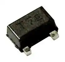
- No. of Pins: 4Pins
- Product Range: -
- Qualification: AEC-Q101
- Power Dissipation: 100mW
- Transistor Mounting: Surface Mount
- Transistor Polarity: NPN
- Transition Frequency: 45GHz
- Transistor Case Style: TSFP
- DC Current Gain hFE Min: 160hFE
- Operating Temperature Max: 150°C
- Continuous Collector Current: 25mA
- Collector Emitter Voltage Max: 4.7V
| Delivery and price | |
|---|---|
| Units per pack | 3000 |
| Price | 0.157 € |
| Current stock | 10+ |
| Lead time | 30 days |
## BFP720F

Low Noise Silicon Germanium Bipolar RF Transistor

## Data Sheet

Revision 1.1, 2012-10-25

RF & Protection Devices ~~eee~~

## **Edition 2012-10-25**

**Published by Infineon Technologies AG 81726 Munich, Germany © 2013 Infineon Technologies AG All Rights Reserved.**

## **Legal Disclaimer**

The information given in this document shall in no event be regarded as a guarantee of conditions or characteristics. With respect to any examples or hints given herein, any typical values stated herein and/or any information regarding the application of the device, Infineon Technologies hereby disclaims any and all warranties and liabilities of any kind, including without limitation, warranties of non-infringement of intellectual property rights of any third party.

## **Information**

For further information on technology, delivery terms and conditions and prices, please contact the nearest Infineon Technologies Office ( **www.infineon.com** ).

## **Warnings**

Due to technical requirements, components may contain dangerous substances. For information on the types in question, please contact the nearest Infineon Technologies Office.

Infineon Technologies components may be used in life-support devices or systems only with the express written approval of Infineon Technologies, if a failure of such components can reasonably be expected to cause the failure of that life-support device or system or to affect the safety or effectiveness of that device or system. Life support devices or systems are intended to be implanted in the human body or to support and/or maintain and sustain and/or protect human life. If they fail, it is reasonable to assume that the health of the user or other persons may be endangered.

**BFP720F**

**==> picture [131 x 63] intentionally omitted <==**

## **BFP720F, Low Noise Silicon Germanium Bipolar RF Transistor**

## **Revision History: 2012-10-25, Revision 1.1**

|**Page**|**Subjects (changes since previous revision)**|
|---|---|
||This data sheet replaces the revision from 2009-03-13.<br>The product itself has not been changed and the device characteristics remain unchanged.<br>Only the product description and information available in the data sheet have been expanded<br>and updated.|
|||
|||
|||
|||


## **Trademarks of Infineon Technologies AG**

AURIX™, C166™, CanPAK™, CIPOS™, CIPURSE™, EconoPACK™, CoolMOS™, CoolSET™, CORECONTROL™, CROSSAVE™, DAVE™, DI-POL™, EasyPIM™, EconoBRIDGE™, EconoDUAL™, EconoPIM™, EconoPACK™, EiceDRIVER™, eupec™, FCOS™, HITFET™, HybridPACK™, I²RF™, ISOFACE™, IsoPACK™, MIPAQ™, ModSTACK™, my-d™, NovalithIC™, OptiMOS™, ORIGA™, POWERCODE™; PRIMARION™, PrimePACK™, PrimeSTACK™, PRO-SIL™, PROFET™, RASIC™, ReverSave™, SatRIC™, SIEGET™, SINDRION™, SIPMOS™, SmartLEWIS™, SOLID FLASH™, TEMPFET™, thinQ!™, TRENCHSTOP™, TriCore™.

## **Other Trademarks**

Advance Design System™ (ADS) of Agilent Technologies, AMBA™, ARM™, MULTI-ICE™, KEIL™, PRIMECELL™, REALVIEW™, THUMB™, µVision™ of ARM Limited, UK. AUTOSAR™ is licensed by AUTOSAR development partnership. Bluetooth™ of Bluetooth SIG Inc. CAT-iq™ of DECT Forum. COLOSSUS™, FirstGPS™ of Trimble Navigation Ltd. EMV™ of EMVCo, LLC (Visa Holdings Inc.). EPCOS™ of Epcos AG. FLEXGO™ of Microsoft Corporation. FlexRay™ is licensed by FlexRay Consortium. HYPERTERMINAL™ of Hilgraeve Incorporated. IEC™ of Commission Electrotechnique Internationale. IrDA™ of Infrared Data Association Corporation. ISO™ of INTERNATIONAL ORGANIZATION FOR STANDARDIZATION. MATLAB™ of MathWorks, Inc. MAXIM™ of Maxim Integrated Products, Inc. MICROTEC™, NUCLEUS™ of Mentor Graphics Corporation. MIPI™ of MIPI Alliance, Inc. MIPS™ of MIPS Technologies, Inc., USA. muRata™ of MURATA MANUFACTURING CO., MICROWAVE OFFICE™ (MWO) of Applied Wave Research Inc., OmniVision™ of OmniVision Technologies, Inc. Openwave™ Openwave Systems Inc. RED HAT™ Red Hat, Inc. RFMD™ RF Micro Devices, Inc. SIRIUS™ of Sirius Satellite Radio Inc. SOLARIS™ of Sun Microsystems, Inc. SPANSION™ of Spansion LLC Ltd. Symbian™ of Symbian Software Limited. TAIYO YUDEN™ of Taiyo Yuden Co. TEAKLITE™ of CEVA, Inc. TEKTRONIX™ of Tektronix Inc. TOKO™ of TOKO KABUSHIKI KAISHA TA. UNIX™ of X/Open Company Limited. VERILOG™, PALLADIUM™ of Cadence Design Systems, Inc. VLYNQ™ of Texas Instruments Incorporated. VXWORKS™, WIND RIVER™ of WIND RIVER SYSTEMS, INC. ZETEX™ of Diodes Zetex Limited.

Last Trademarks Update 2011-11-11

Data Sheet

3

Revision 1.1, 2012-10-25

||**BFP720F**|
|---|---|
||**Table of Contents**|
|**Table**|**of Contents**|
||**Table of Contents**. . . . . . . . . . . . . . . . . . . . . . . . . . . . . . . . . . . . . . . . . . . . . . . . . . . . . . . . . . . . . . . .  4|
||**List of Figures**. . . . . . . . . . . . . . . . . . . . . . . . . . . . . . . . . . . . . . . . . . . . . . . . . . . . . . . . . . . . . . . . . . .  5|
||**List of Tables**. . . . . . . . . . . . . . . . . . . . . . . . . . . . . . . . . . . . . . . . . . . . . . . . . . . . . . . . . . . . . . . . . . . .  6|
|**1**|**Product Brief**. . . . . . . . . . . . . . . . . . . . . . . . . . . . . . . . . . . . . . . . . . . . . . . . . . . . . . . . . . . . . . . . . . . .  7|
|**2**|**Features**. . . . . . . . . . . . . . . . . . . . . . . . . . . . . . . . . . . . . . . . . . . . . . . . . . . . . . . . . . . . . . . . . . . . . . . .  8|
|**3**|**Maximum Ratings**. . . . . . . . . . . . . . . . . . . . . . . . . . . . . . . . . . . . . . . . . . . . . . . . . . . . . . . . . . . . . . . .  9|
|**4**|**Thermal Characteristics**. . . . . . . . . . . . . . . . . . . . . . . . . . . . . . . . . . . . . . . . . . . . . . . . . . . . . . . . . .  10|
|**5**|**Electrical Characteristics**. . . . . . . . . . . . . . . . . . . . . . . . . . . . . . . . . . . . . . . . . . . . . . . . . . . . . . . . .  12|
|5.1|DC Characteristics  . . . . . . . . . . . . . . . . . . . . . . . . . . . . . . . . . . . . . . . . . . . . . . . . . . . . . . . . . . . . . . .  12|
|5.2|General AC Characteristics  . . . . . . . . . . . . . . . . . . . . . . . . . . . . . . . . . . . . . . . . . . . . . . . . . . . . . . . .  12|
|5.3|Frequency Dependent AC Characteristics . . . . . . . . . . . . . . . . . . . . . . . . . . . . . . . . . . . . . . . . . . . . .  13|
|5.4|Characteristic Curves . . . . . . . . . . . . . . . . . . . . . . . . . . . . . . . . . . . . . . . . . . . . . . . . . . . . . . . . . . . . .  18|
|**6**|**Simulation Data**. . . . . . . . . . . . . . . . . . . . . . . . . . . . . . . . . . . . . . . . . . . . . . . . . . . . . . . . . . . . . . . . .  23|
|**7**|**Package Information TSFP-4-1**. . . . . . . . . . . . . . . . . . . . . . . . . . . . . . . . . . . . . . . . . . . . . . . . . . . .  24|


Data Sheet

Revision 1.1, 2012-10-25

4

**BFP720F**

**==> picture [131 x 63] intentionally omitted <==**

## **List of Figures**

## **List of Figures**

|Figure|4-1|Total Power Dissipation_P_tot=_f_(_T_s) . . . . . . . . . . . . . . . . . . . . . . . . . . . . . . . . . . . . . . . . . . . . . . . .  10|
|---|---|---|
|Figure|4-2|Permissible Pulse Load_P_tot_max/_P_tot_DC=_f_(_t_p) . . . . . . . . . . . . . . . . . . . . . . . . . . . . . . . . . . . . . . .  11|
|Figure|4-3|Permissible Pulse Load_R_thJS=_f_(_t_p). . . . . . . . . . . . . . . . . . . . . . . . . . . . . . . . . . . . . . . . . . . . . . . .  11|
|Figure|5-1|BFP720F Testing Circuit. . . . . . . . . . . . . . . . . . . . . . . . . . . . . . . . . . . . . . . . . . . . . . . . . . . . . . . . .  13|
|Figure|5-2|Transition Frequency_f_T=_f_(_I_C,_V_CE),_f_= 1 GHz,_V_CEParameter in V. . . . . . . . . . . . . . . . . . . . . . .  18|
|Figure|5-3|Power Gain_G_ma,_G_ms, I_S_21I² =_f_(_f_),_V_CE= 3 V,_I_C= 13 mA . . . . . . . . . . . . . . . . . . . . . . . . . . . . . . .  18|
|Figure|5-4|Power Gain_G_ma,_G_ms=_f_(_I_C),_V_CE= 3 V,_f_= Parameter in GHz. . . . . . . . . . . . . . . . . . . . . . . . . . .  19|
|Figure|5-5|Power Gain_G_ma,_G_ms=_f_(_V_CE),_I_C= 13 mA,_f_= Parameter in GHz . . . . . . . . . . . . . . . . . . . . . . . .  19|
|Figure|5-6|Input Matching_S_11 _= f_(_f_),_V_CE= 3 V,_I_C= 5 mA / 13 mA . . . . . . . . . . . . . . . . . . . . . . . . . . . . . . . .  20|
|Figure|5-7|Output Matching_S_22 _= f_(_f_),_V_CE= 3 V,_I_C= 5 mA / 13 mA . . . . . . . . . . . . . . . . . . . . . . . . . . . . . . .  20|
|Figure|5-8|Source Impedance_Z_optfor_NF_min_= f_(_f_),_V_CE= 3 V,_I_C= 5 mA / 13 mA  . . . . . . . . . . . . . . . . . . . . .  21|
|Figure|5-9|Noise Figure_NF_min=_f_(_I_C),_V_CE= 3 V,_Z_S=_Z_opt. . . . . . . . . . . . . . . . . . . . . . . . . . . . . . . . . . . . . . .  21|
|Figure|5-10|Noise Figure_NF_min=_f_(_f_),_V_CE= 3 V,_Z_S=_Z_opt. . . . . . . . . . . . . . . . . . . . . . . . . . . . . . . . . . . . . . . .  22|
|Figure|7-1|Package Outline . . . . . . . . . . . . . . . . . . . . . . . . . . . . . . . . . . . . . . . . . . . . . . . . . . . . . . . . . . . . . . .  24|
|Figure|7-2|Footprint . . . . . . . . . . . . . . . . . . . . . . . . . . . . . . . . . . . . . . . . . . . . . . . . . . . . . . . . . . . . . . . . . . . . .  24|
|Figure|7-3|Marking Description (Marking BFP720F: R9s) . . . . . . . . . . . . . . . . . . . . . . . . . . . . . . . . . . . . . . . .  24|
|Figure|7-4|Tape Dimensions . . . . . . . . . . . . . . . . . . . . . . . . . . . . . . . . . . . . . . . . . . . . . . . . . . . . . . . . . . . . . .  24|


Data Sheet

Revision 1.1, 2012-10-25

5

**BFP720F**

**==> picture [131 x 63] intentionally omitted <==**

## **List of Tables**

## **List of Tables**

|Table|3-1|Maximum Ratings at_T_A= 25 °C (unless otherwise specified) . . . . . . . . . . . . . . . . . . . . . . . . . . . . .  9|
|---|---|---|
|Table|4-1|Thermal Resistance  . . . . . . . . . . . . . . . . . . . . . . . . . . . . . . . . . . . . . . . . . . . . . . . . . . . . . . . . . . .  10|
|Table|5-1|DC Characteristics at_T_A= 25 °C . . . . . . . . . . . . . . . . . . . . . . . . . . . . . . . . . . . . . . . . . . . . . . . . . .  12|
|Table|5-2|AC Characteristics at_T_A= 25 °C . . . . . . . . . . . . . . . . . . . . . . . . . . . . . . . . . . . . . . . . . . . . . . . . . .  12|
|Table|5-3|AC Characteristics,_V_CE= 3 V,_f_= 150 MHz . . . . . . . . . . . . . . . . . . . . . . . . . . . . . . . . . . . . . . . . .  13|
|Table|5-4|AC Characteristics_, V_CE= 3 V,_f_= 450 MHz . . . . . . . . . . . . . . . . . . . . . . . . . . . . . . . . . . . . . . . . .  14|
|Table|5-5|AC Characteristics_, V_CE= 3 V,_f_= 900 MHz . . . . . . . . . . . . . . . . . . . . . . . . . . . . . . . . . . . . . . . . .  14|
|Table|5-6|AC Characteristics,_V_CE= 3 V,_f_= 1.5 GHz . . . . . . . . . . . . . . . . . . . . . . . . . . . . . . . . . . . . . . . . . .  15|
|Table|5-7|AC Characteristics,_V_CE= 3 V,_f_= 1.9 GHz . . . . . . . . . . . . . . . . . . . . . . . . . . . . . . . . . . . . . . . . . .  15|
|Table|5-8|AC Characteristics_, V_CE= 3 V,_f_= 2.4 GHz . . . . . . . . . . . . . . . . . . . . . . . . . . . . . . . . . . . . . . . . . .  16|
|Table|5-9|AC Characteristics,_V_CE= 3 V,_f_= 3.5 GHz . . . . . . . . . . . . . . . . . . . . . . . . . . . . . . . . . . . . . . . . . .  16|
|Table|5-10|AC Characteristics,_V_CE= 3 V,_f_= 5.5 GHz . . . . . . . . . . . . . . . . . . . . . . . . . . . . . . . . . . . . . . . . . .  17|
|Table|5-11|AC Characteristics,_V_CE= 3 V,_f_= 10 GHz . . . . . . . . . . . . . . . . . . . . . . . . . . . . . . . . . . . . . . . . . .  17|


Data Sheet

6

Revision 1.1, 2012-10-25

**BFP720F**

**==> picture [131 x 63] intentionally omitted <==**

**Product Brief**

## **1 Product Brief**

The BFP720F is a very low noise wideband NPN bipolar RF transistor. The device is based on Infineon’s reliable high volume silicon germanium carbon (SiGe:C) heterojunction bipolar technology. The collector design supports voltages up to _V_ CEO = 4.0 V and currents up to _I_ C = 25 mA. The device is especially suited for mobile applications in which low power consumption is a key requirement. The typical transition frequency is approximately 45 GHz, hence the device offers high power gain at frequencies up to 12 GHz in amplifier applications. The device is housed in a thin small flat plastic package with visible leads.

Data Sheet

Revision 1.1, 2012-10-25

7

**BFP720F**

## **Features**

## **2 Features**

- High performance general purpose wideband LNA transistor

- Operation voltage: 1.0 V to 4.0 V

- Transistor geometry optimized for low current applications

- 26.5 dB maximum stable gain at 1.9 GHz and only 13 mA

- 15 dB maximum available gain at 10 GHz and only 13 mA

- 0.7 dB minimum noise figure at 5.5 GHz and 1.0 dB at 10 GHz

- High linearity _OP_ 1dB = 7 dBm and _OIP_ 3 = 21 dBm at 5.5 GHz and low current consumption of 13 mA

- Thin small flat Pb-free (RoHS compliant) and halogen-free package with visible leads

- Qualification report according to AEC-Q101 available

## **Applications**

FM Radio, Mobile TV, RKE, AMR, Cellular, ZigBee, GPS, WiMAX, SDARs, Satellite Radio, Bluetooth, WiFi, Cordless phone, UMTS, WLAN, UWB, LNB

## _**Attention: ESD (Electrostatic discharge) sensitive device, observe handling precautions**_

|**Product Name**|**Package**|**Pin Configuration**|**Pin Configuration**|**Pin Configuration**|**Pin Configuration**|**Marking**|
|---|---|---|---|---|---|---|
|BFP720F|TSFP-4-1|1 = B|2 = E|3 = C|4 = E|R9s|


Data Sheet

8

Revision 1.1, 2012-10-25

**BFP720F**

**==> picture [131 x 63] intentionally omitted <==**

## **Maximum Ratings**

## **3 Maximum Ratings**

**Table 3-1 Maximum Ratings at** _**T**_ **A = 25 °C (unless otherwise specified)**

|**Parameter**|**Symbol**|**Values**|**Values**|**Values**|**Unit**|**Note /**<br>**Test Condition**|
|---|---|---|---|---|---|---|
|||**Min.**|**Typ.**|**Max.**|||
|Collector emitter voltage|_V_CEO|||4.0<br>3.5|V|Open base<br>_T_A= 25 °C<br>_T_A= -55 °C|
|Collector emitter voltage|_V_CES|–|–|13|V|E-B short circuited|
|Collector base voltage|_V_CBO|–|–|13|V|Open emitter|
|Emitter base voltage|_V_EBO|–|–|1.2|V|Open collector|
|Collector current|_I_C|–|–|25|mA||
|Base current|_I_B|–|–|2|mA||
|Total power dissipation1)|_P_tot|–|–|100|mW|_T_S ≤109 °C|
|Junction temperature|_T_J|–|–|150|°C||
|Storage temperature|_T_Stg|-55|–|150|°C||


1) _T_ S is the soldering point temperature. _T_ S is measured on the emitter lead at the soldering point to the pcb

_**Attention: Stresses above the max. values listed here may cause permanent damage to the device. Exposure to absolute maximum rating conditions for extended periods may affect device reliability. Maximum ratings are absolute ratings; exceeding only one of these values may cause irreversible damage to the integrated circuit.**_

Data Sheet

9

Revision 1.1, 2012-10-25

**BFP720F**

**==> picture [131 x 63] intentionally omitted <==**

## **Thermal Characteristics**

## **4 Thermal Characteristics**

## **Table 4-1 Thermal Resistance**

|**Parameter**|**Symbol**|**Values**|**Values**|**Values**|**Unit**|**Note / Test Condition**|
|---|---|---|---|---|---|---|
|||**Min.**|**Typ.**|**Max.**|||
|Junction - soldering point1)|_R_thJS|–|410|–|K/W|–|
|1)For the definition of_R_thJSplease refer to Application Note AN077 (Thermal Resistance Calculation)|||||||


**==> picture [261 x 261] intentionally omitted <==**

**----- Start of picture text -----**<br>
120<br>100<br>80<br>60<br>40<br>20<br>0<br>0 50 100 150<br>Ts [°C]<br>Ptot[mW]<br>**----- End of picture text -----**<br>


**Figure 4-1 Total Power Dissipation** _**P**_ **tot =** _**f**_ **(** _**T**_ **s)**

Data Sheet

10

Revision 1.1, 2012-10-25

**BFP720F**

## **Thermal Characteristics**

**==> picture [240 x 557] intentionally omitted <==**

**----- Start of picture text -----**<br>
10<br>D= 0<br>D= .005<br>D= .01<br>D= .02<br>SY i D= .05<br>D= .1<br>D= .2<br>D= .5<br>D=0<br>M7 ||<br>D=0.5<br>We<br>1 so<br>|<br>tp [sec]<br>P tot_max /  /  P tot_DC =  =  f  ( t p))<br>1000<br>mas<br>D=0.5<br>i A053aio<br>7focccl<br>Dal D= .5 bil<br>D= .2<br>D= .1<br>D= .05<br>A II ||<br>D= .02<br>D= .01<br>D=0<br>D= .005<br>D= 0<br>ilea l<br>100<br>tp [sec]<br>Ptot_max / Ptot_DC<br>1.E-07 1.E-06 1.E-05 1.E-04 1.E-03 1.E-02 1.E-01 1.E+00<br>RthJS [K/W]<br>1.E-07 1.E-06 1.E-05 1.E-04 1.E-03 1.E-02 1.E-01 1.E+00<br>**----- End of picture text -----**<br>


**Figure 4-2 Permissible Pulse Load** _**P**_ **tot_max /  /** _**P**_ **tot_DC =  =** _**f**_ **(** _**t**_ **p))**

**Figure 4-3 Permissible Pulse Load** _**R**_ **thJS =** _**f**_ **(** _**t**_ **p)**

Data Sheet

11

Revision 1.1, 2012-10-25

**BFP720F**

**==> picture [131 x 63] intentionally omitted <==**

## **Electrical Characteristics**

## **5 Electrical Characteristics**

## **5.1 DC Characteristics**

## **Table 5-1 DC Characteristics at** _**T**_ **A = 25 °C**

|**Table 5-1**<br>**DC Characteristics at****_T_A**|**= 25 °C**||||||
|---|---|---|---|---|---|---|
|**Parameter**|**Symbol**|**Values**|||**Unit**|**Note / Test Condition**|
|||**Min.**|**Typ.**|**Max.**|||
|Collector emitter breakdown voltage|_V_(BR)CEO|4|4.7|–|V|_I_C = 1 mA,_I_B = 0 mA|
|Collector emitter cutoff current|_I_CES|–|–|30|μA|_V_CE = 13 V,_V_BE = 0 V|
|Collector base cutoff current|_I_CBO|–|–|100|nA|_V_CB = 5 V,_I_E = 0 mA|
|Emitter base cutoff current|_I_EBO|–|–|2|μA|_V_EB = 0.5 V,_I_C = 0 mA|
|DC current gain|_h_FE|160|250|400||_I_C= 13 mA,_V_CE= 3 V<br>pulse measured|


## **5.2 General AC Characteristics**

**Table 5-2 AC Characteristics at** _**T**_ **A = 25 °C**

|**Table 5-2**<br>**AC Characteristics at****_T_A**|**= 25 °C**||||||
|---|---|---|---|---|---|---|
|**Parameter**|**Symbol**|**Values**|||**Unit**|**Note / Test Condition**|
|||**Min.**|**Typ.**|**Max.**|||
|Transition frequency|_f_T|–|45|–|GHz|_I_C= 13 mA,_V_CE= 3 V<br>_f_= 1 GHz|
|Collector base capacitance|_C_CB|–|0.06|–|pF|_V_CB= 3 V,_V_BE= 0 V<br>_f_= 1 MHz<br>emitter grounded|
|Collector emitter capacitance|_C_CE|–|0.3|–|pF|_V_CE= 3 V,_V_BE= 0 V<br>_f_= 1 MHz<br>base grounded|
|Emitter base capacitance|_C_EB|–|0.3|–|pF|_V_EB= 0.5 V,_V_CB= 0 V<br>_f_= 1 MHz<br>collector grounded|


Data Sheet

12

Revision 1.1, 2012-10-25

**BFP720F**

**==> picture [131 x 63] intentionally omitted <==**

## **Electrical Characteristics**

## **5.3 Frequency Dependent AC Characteristics**

Measurement setup is a test fixture with Bias T’s in a 50 Ω system, _T_ A = 25 °C

**==> picture [464 x 199] intentionally omitted <==**

**----- Start of picture text -----**<br>
VC<br>Top View<br>Bias-T<br>OUT<br>E C<br>VB<br>B E<br>Bias-T (Pin 1)<br>IN<br>**----- End of picture text -----**<br>


## **Figure 5-1 BFP720F Testing Circuit**

**Table 5-3 AC Characteristics,** _**V**_ **CE = 3 V,** _**f**_ **= 150 MHz**

|**Table 5-3**<br>**AC Characteristics,****_V_CE**|**= 3 V,****_f_ = 1**|**50 MHz**|**50 MHz**|**50 MHz**|||
|---|---|---|---|---|---|---|
|**Parameter**|**Symbol**|**Values**|||**Unit**|**Note / Test Condition**|
|||**Min.**|**Typ.**|**Max.**|||
|**Maximum Power Gain**<br>Low noise operation point<br>High linearity operation point|_G_ms<br>_G_ms|–<br>–|34<br>37.5|–<br>–|dB|_I_C= 5 mA<br>_I_C = 13 mA|
|**Transducer Gain**<br>Low noise operation point<br>High linearity operation point|_S_21<br>_S_21|–<br>–|23<br>29|–<br>–|dB|_Z_S=_Z_L=50Ω<br>_I_C= 5 mA<br>_I_C = 13 mA|
|**Minimum Noise Figure**<br>Minimum noise figure<br>Associated gain|_NF_min<br>_G_ass|–<br>–|0.4<br>28|–<br>–|dB|_Z_S=_Z_opt<br>_I_C= 5 mA<br>_I_C = 5 mA|
|**Linearity**<br>1 dB gain compression point<br>3rd order intercept point|_OP_1dB<br>_OIP_3|–<br>–|6<br>22.5|–<br>–|dBm|_Z_S=_Z_L=50Ω<br>_I_C= 13 mA<br>_I_C = 13 mA|


Data Sheet

13

Revision 1.1, 2012-10-25

**BFP720F**

**==> picture [131 x 63] intentionally omitted <==**

## **Electrical Characteristics**

**Table 5-4 AC Characteristics** _**, V**_ **CE = 3 V,** _**f**_ **= 450 MHz**

|**Parameter**|**Symbol**|**Values**|**Values**|**Values**|**Unit**|**Note / Test Condition**|
|---|---|---|---|---|---|---|
|||**Min.**|**Typ.**|**Max.**|||
|**Maximum Power Gain**<br>Low noise operation point<br>High linearity operation point|_G_ms<br>_G_ms|–<br>–|29<br>32.5|–<br>–|dB|_I_C= 5 mA<br>_I_C = 13 mA|
|**Transducer Gain**<br>Low noise operation point<br>High linearity operation point|_S_21<br>_S_21|–<br>–|22.5<br>28.5|–<br>–|dB|_Z_S=_Z_L=50Ω<br>_I_C= 5 mA<br>_I_C = 13 mA|
|**Minimum Noise Figure**<br>Minimum noise figure<br>Associated gain|_NF_min<br>_G_ass|–<br>–|0.4<br>27.5|–<br>–|dB|_Z_S=_Z_opt<br>_I_C= 5 mA<br>_I_C = 5 mA|
|**Linearity**<br>1 dB gain compression point<br>3rd order intercept point|_OP_1dB<br>_OIP_3|–<br>–|5.5<br>21.5|–<br>–|dBm|_Z_S=_Z_L=50Ω<br>_I_C= 13 mA<br>_I_C = 13 mA|


## **Table 5-5 AC Characteristics** _**, V**_ **CE = 3 V,** _**f**_ **= 900 MHz**

|**Parameter**|**Symbol**|**Values**|**Values**|**Values**|**Unit**|**Note / Test Condition**|
|---|---|---|---|---|---|---|
|||**Min.**|**Typ.**|**Max.**|||
|**Maximum Power Gain**<br>Low noise operation point<br>High linearity operation point|_G_ms<br>_G_ms|–<br>–|26.5<br>29.5|–<br>–|dB|_I_C= 5 mA<br>_I_C = 13 mA|
|**Transducer Gain**<br>Low noise operation point<br>High linearity operation point|_S_21<br>_S_21|–<br>–|22.5<br>27.5|–<br>–|dB|_Z_S=_Z_L=50Ω<br>_I_C= 5 mA<br>_I_C = 13 mA|
|**Minimum Noise Figure**<br>Minimum noise figure<br>Associated gain|_NF_min<br>_G_ass|–<br>–|0.45<br>25.5|–<br>–|dB|_Z_S=_Z_opt<br>_I_C= 5 mA<br>_I_C = 5 mA|
|**Linearity**<br>1 dB gain compression point<br>3rd order intercept point|_OP_1dB<br>_OIP_3|–<br>–|5.5<br>20.5|–<br>–|dBm|_Z_S=_Z_L=50Ω<br>_I_C= 13 mA<br>_I_C = 13 mA|


Data Sheet

14

Revision 1.1, 2012-10-25

**BFP720F**

**==> picture [131 x 63] intentionally omitted <==**

## **Electrical Characteristics**

**Table 5-6 AC Characteristics,** _**V**_ **CE = 3 V,** _**f**_ **= 1.5 GHz**

|**Parameter**|**Symbol**|**Values**|**Values**|**Values**|**Unit**|**Note / Test Condition**|
|---|---|---|---|---|---|---|
|||**Min.**|**Typ.**|**Max.**|||
|**Maximum Power Gain**<br>Low noise operation point<br>High linearity operation point|_G_ms<br>_G_ms|–<br>–|24<br>27.5|–<br>–|dB|_I_C= 5 mA<br>_I_C = 13 mA|
|**Transducer Gain**<br>Low noise operation point<br>High linearity operation point|_S_21<br>_S_21|–<br>–|21.5<br>26|–<br>–|dB|_Z_S=_Z_L=50Ω<br>_I_C= 5 mA<br>_I_C = 13 mA|
|**Minimum Noise Figure**<br>Minimum noise figure<br>Associated gain|_NF_min<br>_G_ass|–<br>–|0.45<br>24|–<br>–|dB|_Z_S=_Z_opt<br>_I_C= 5 mA<br>_I_C = 5 mA|
|**Linearity**<br>1 dB gain compression point<br>3rd order intercept point|_OP_1dB<br>_OIP_3|–<br>–|6<br>21|–<br>–|dBm|_Z_S=_Z_L=50Ω<br>_I_C= 13 mA<br>_I_C = 13 mA|


## **Table 5-7 AC Characteristics,** _**V**_ **CE = 3 V,** _**f**_ **= 1.9 GHz**

|**Parameter**|**Symbol**|**Values**|**Values**|**Values**|**Unit**|**Note / Test Condition**|
|---|---|---|---|---|---|---|
|||**Min.**|**Typ.**|**Max.**|||
|**Maximum Power Gain**<br>Low noise operation point<br>High linearity operation point|_G_ms<br>_G_ms|–<br>–|23<br>26.5|–<br>–|dB|_I_C= 5 mA<br>_I_C = 13 mA|
|**Transducer Gain**<br>Low noise operation point<br>High linearity operation point|_S_21<br>_S_21|–<br>–|21<br>24.5|–<br>–|dB|_Z_S=_Z_L=50Ω<br>_I_C= 5 mA<br>_I_C = 13 mA|
|**Minimum Noise Figure**<br>Minimum noise figure<br>Associated gain|_NF_min<br>_G_ass|–<br>–|0.5<br>23|–<br>–|dB|_Z_S=_Z_opt<br>_I_C= 5 mA<br>_I_C = 5 mA|
|**Linearity**<br>1 dB gain compression point<br>3rd order intercept point|_OP_1dB<br>_OIP_3|–<br>–|6.5<br>21|–<br>–|dBm|_Z_S=_Z_L=50Ω<br>_I_C= 13 mA<br>_I_C = 13 mA|


Data Sheet

15

Revision 1.1, 2012-10-25

**BFP720F**

**==> picture [131 x 63] intentionally omitted <==**

## **Electrical Characteristics**

## **Table 5-8 AC Characteristics** _**, V**_ **CE = 3 V,** _**f**_ **= 2.4 GHz**

|**Parameter**|**Symbol**|**Values**|**Values**|**Values**|**Unit**|**Note / Test Condition**|
|---|---|---|---|---|---|---|
|||**Min.**|**Typ.**|**Max.**|||
|**Maximum Power Gain**<br>Low noise operation point<br>High linearity operation point|_G_ms<br>_G_ms|–<br>–|22<br>25.5|–<br>–|dB|_I_C= 5 mA<br>_I_C = 13 mA|
|**Transducer Gain**<br>Low noise operation point<br>High linearity operation point|_S_21<br>_S_21|–<br>–|20.5<br>23|–<br>–|dB|_Z_S=_Z_L=50Ω<br>_I_C= 5 mA<br>_I_C = 13 mA|
|**Minimum Noise Figure**<br>Minimum noise figure<br>Associated gain|_NF_min<br>_G_ass|–<br>–|0.55<br>22|–<br>–|dB|_Z_S=_Z_opt<br>_I_C= 5 mA<br>_I_C = 5 mA|
|**Linearity**<br>1 dB gain compression point<br>3rd order intercept point|_OP_1dB<br>_OIP_3|–<br>–|6<br>21|–<br>–|dBm|_Z_S=_Z_L=50Ω<br>_I_C= 13 mA<br>_I_C = 13 mA|


## **Table 5-9 AC Characteristics,** _**V**_ **CE = 3 V,** _**f**_ **= 3.5 GHz**

|**Parameter**|**Symbol**|**Values**|**Values**|**Values**|**Unit**|**Note / Test Condition**|
|---|---|---|---|---|---|---|
|||**Min.**|**Typ.**|**Max.**|||
|**Maximum Power Gain**<br>Low noise operation point<br>High linearity operation point|_G_ms<br>_G_ms|–<br>–|20.5<br>23.5|–<br>–|dB|_I_C= 5 mA<br>_I_C = 13 mA|
|**Transducer Gain**<br>Low noise operation point<br>High linearity operation point|_S_21<br>_S_21|–<br>–|18<br>20.5|–<br>–|dB|_Z_S=_Z_L=50Ω<br>_I_C= 5 mA<br>_I_C = 13 mA|
|**Minimum Noise Figure**<br>Minimum noise figure<br>Associated gain|_NF_min<br>_G_ass|–<br>–|0.6<br>19.5|–<br>–|dB|_Z_S=_Z_opt<br>_I_C= 5 mA<br>_I_C = 5 mA|
|**Linearity**<br>1 dB gain compression point<br>3rd order intercept point|_OP_1dB<br>_OIP_3|–<br>–|6.5<br>21.5|–<br>–|dBm|_Z_S=_Z_L=50Ω<br>_I_C= 13 mA<br>_I_C = 13 mA|


Data Sheet

16

Revision 1.1, 2012-10-25

**BFP720F**

**==> picture [131 x 63] intentionally omitted <==**

## **Electrical Characteristics**

**Table 5-10 AC Characteristics,** _**V**_ **CE = 3 V,** _**f**_ **= 5.5 GHz**

|**Parameter**|**Symbol**|**Values**|**Values**|**Values**|**Unit**|**Note / Test Condition**|
|---|---|---|---|---|---|---|
|||**Min.**|**Typ.**|**Max.**|||
|**Maximum Power Gain**<br>Low noise operation point<br>High linearity operation point|_G_ms<br>_G_ms|–<br>–|19<br>21.5|–<br>–|dB|_I_C= 5 mA<br>_I_C = 13 mA|
|**Transducer Gain**<br>Low noise operation point<br>High linearity operation point|_S_21<br>_S_21|–<br>–|15<br>16.5|–<br>–|dB|_Z_S=_Z_L=50Ω<br>_I_C= 5 mA<br>_I_C = 13 mA|
|**Minimum Noise Figure**<br>Minimum noise figure<br>Associated gain|_NF_min<br>_G_ass|–<br>–|0.7<br>15|–<br>–|dB|_Z_S=_Z_opt<br>_I_C= 5 mA<br>_I_C = 5 mA|
|**Linearity**<br>1 dB gain compression point<br>3rd order intercept point|_OP_1dB<br>_OIP_3|–<br>–|7<br>21|–<br>–|dBm|_Z_S=_Z_L=50Ω<br>_I_C= 13 mA<br>_I_C = 13 mA|


**Table 5-11 AC Characteristics,** _**V**_ **CE = 3 V,** _**f**_ **= 10 GHz**

|**Parameter**|**Symbol**|**Values**|**Values**|**Values**|**Unit**|**Note / Test Condition**|
|---|---|---|---|---|---|---|
|||**Min.**|**Typ.**|**Max.**|||
|**Maximum Power Gain**<br>Low noise operation point<br>High linearity operation point|_G_ma<br>_G_ma|–<br>–|14<br>15|–<br>–|dB|_I_C= 5 mA<br>_I_C = 13 mA|
|**Transducer Gain**<br>Low noise operation point<br>High linearity operation point|_S_21<br>_S_21|–<br>–|9.5<br>10.5|–<br>–|dB|_Z_S=_Z_L=50Ω<br>_I_C= 5 mA<br>_I_C = 13 mA|
|**Minimum Noise Figure**<br>Minimum noise figure<br>Associated gain|_NF_min<br>_G_ass|–<br>–|1.0<br>10.5|–<br>–|dB|_Z_S=_Z_opt<br>_I_C= 5 mA<br>_I_C = 5 mA|
|**Linearity**<br>1 dB gain compression point<br>3rd order intercept point|_OP_1dB<br>_OIP_3|–<br>–|8<br>19.5|–<br>–|dBm|_Z_S=_Z_L=50Ω<br>_I_C= 13 mA<br>_I_C = 13 mA|


## **Notes**

> _1. Gms = IS21 / S12I for k < 1; Gma = IS21 / S12I(k-(k[2] -1)[1/2] ) for k > 1_

_2. In order to get the NF min values stated in this chapter the test fixture losses have been subtracted from all measured results_

Data Sheet

17

Revision 1.1, 2012-10-25

**BFP720F**

**==> picture [131 x 63] intentionally omitted <==**

## **Electrical Characteristics**

## **5.4 Characteristic Curves**

**==> picture [253 x 272] intentionally omitted <==**

**----- Start of picture text -----**<br>
50<br>45<br> 3.00V<br>40<br>35<br> 2.00V<br>30<br>25<br>20<br> 1.50V<br>15<br>10<br> 1.00V<br>5<br> 0.50V<br>0<br>0 1 2<br>10 10 10<br>IC [mA]<br> [GHz]fT<br>**----- End of picture text -----**<br>


**Figure 5-2 Transition Frequency** _**f**_ **T =** _**f**_ **(** _**I**_ **C,** _**V**_ **CE),** _**f**_ **= 1 GHz,** _**V**_ **CE Parameter in V**

**==> picture [258 x 286] intentionally omitted <==**

**----- Start of picture text -----**<br>
42<br>40<br>38<br>36<br>34<br>32<br>30<br>G<br>28 ms<br>26<br>24<br>22<br>20<br>18 |S21| [2] Gma<br>16<br>14<br>12<br>10<br>8<br>6<br>0 1 2 3 4 5 6 7 8 9 10<br>f [GHz]<br>G [dB]<br>**----- End of picture text -----**<br>


**Figure 5-3 Power Gain** _**G**_ **ma,** _**G**_ **ms, I** _**S**_ **21I² =** _**f**_ **(** _**f**_ **),** _**V**_ **CE = 3 V,** _**I**_ **C = 13 mA**

Data Sheet

18

Revision 1.1, 2012-10-25

**BFP720F**

**==> picture [131 x 63] intentionally omitted <==**

## **Electrical Characteristics**

**==> picture [268 x 294] intentionally omitted <==**

**----- Start of picture text -----**<br>
42<br>40<br> 0.15GHz<br>38<br>36<br> 0.45GHz<br>34<br>32<br> 0.90GHz<br>30<br> 1.50GHz<br>28  1.90GHz<br> 2.40GHz<br>26<br> 3.50GHz<br>24<br>22<br> 5.50GHz<br>20<br>18<br>16<br> 10.00GHz<br>14<br>12<br>10<br>0 5 10 15 20 25 30<br>IC [mA]<br>G [dB]<br>**----- End of picture text -----**<br>


**Figure 5-4 Power Gain** _**G**_ **ma,** _**G**_ **ms =** _**f**_ **(** _**I**_ **C),** _**V**_ **CE = 3 V,** _**f**_ **= Parameter in GHz**

**==> picture [266 x 295] intentionally omitted <==**

**----- Start of picture text -----**<br>
40<br>38  0.15GHz<br>36<br>34<br> 0.45GHz<br>32<br>30  0.90GHz<br>28  1.50GHz<br> 1.90GHz<br>26  2.40GHz<br>24  3.50GHz<br>22  5.50GHz<br>20<br>18<br>16<br> 10.00GHz<br>14<br>12<br>10<br>8<br>6<br>0 0.5 1 1.5 2 2.5 3 3.5 4 4.5 5<br>VCE [V]<br>G [dB]<br>**----- End of picture text -----**<br>


**Figure 5-5 Power Gain** _**G**_ **ma,** _**G**_ **ms =** _**f**_ **(** _**V**_ **CE),** _**I**_ **C = 13 mA,** _**f**_ **= Parameter in GHz**

Data Sheet

19

Revision 1.1, 2012-10-25

**BFP720F**

**==> picture [131 x 63] intentionally omitted <==**

## **Electrical Characteristics**

**==> picture [277 x 270] intentionally omitted <==**

**----- Start of picture text -----**<br>
Swp Max<br>10GHz<br>10 GHz<br>10 GHz<br>9 GHz<br>9 GHz S11 @ 3V, 13mA<br>8 GHz<br>S11 @ 3V, 5mA<br>8 GHz<br>7 GHz<br>6 GHz<br>7 GHz 10 MHz<br>5 GHz<br>4 GHz<br>6 GHz 3 GHz<br>5 GHz<br>2 GHz<br>4 GHz<br>1 GHz<br>1 GHz<br>3 GHz<br>2 GHz<br>Swp Min<br>0GHz<br>10.0<br>5.0<br>-0.2<br>4.0<br>3.0<br>-0.4<br>2.0<br>-0.6<br>-0.8<br>1.0<br>0 0.2 0.4 0.6 0.8 1.0 2.0 3.0 4.0 5.0 10.0<br>-1.0<br>0.8<br>0.6<br>-2.0<br>0.4<br>-3.0<br>-4.0<br>0.2<br>-5.0<br>-10.0<br>**----- End of picture text -----**<br>


**Figure 5-6 Input Matching** _**S**_ **11** _**= f**_ **(** _**f**_ **),** _**V**_ **CE = 3 V,** _**I**_ **C = 5 mA / 13 mA**

**==> picture [305 x 284] intentionally omitted <==**

**----- Start of picture text -----**<br>
Swp Max<br>10GHz<br>S22 @ 3V, 13mA<br>S22 @ 3V, 5mA<br>10 GHz<br>10 MHz<br>10 GHz<br>9 GHz<br>9 GHz<br>8 GHz<br>7 GHz<br>8 GHz 6 GHz<br>5 GHz<br>4 GHz<br>7 GHz 3 GHz<br>1 GHz 1 GHz<br>6 GHz 2 GHz<br>5 GHz<br>4 GHz<br>3 GHz 2 GHz<br>Swp Min<br>0GHz<br>10.0<br>5.0<br>-0.2<br>4.0<br>3.0<br>-0.4<br>2.0<br>-0.6<br>-0.8<br>1.0<br>0 0.2 0.4 0.6 0.8 1.0 2.0 3.0 4.0 5.0 10.0<br>-1.0<br>0.8<br>0.6<br>-2.0<br>0.4<br>-3.0<br>-4.0<br>0.2<br>-5.0<br>-10.0<br>**----- End of picture text -----**<br>


**Figure 5-7 Output Matching** _**S**_ **22** _**= f**_ **(** _**f**_ **),** _**V**_ **CE = 3 V,** _**I**_ **C = 5 mA / 13 mA**

Data Sheet

20

Revision 1.1, 2012-10-25

**BFP720F**

**==> picture [131 x 63] intentionally omitted <==**

## **Electrical Characteristics**

**==> picture [497 x 636] intentionally omitted <==**

**----- Start of picture text -----**<br>
Swp Max<br>10GHz<br>5.5GHz<br>Δ :  Ic = 13mA<br>Δ :  Ic = 13mA<br>� :  Ic = 5mA 2.4GHz<br>� :  Ic = 5mA 1.9GHz<br>2.4GHz<br>5.5GHz 1.9GHz<br>0.9GHz<br>0.45GHz<br>10GHz<br>Swp Min<br>0.45GHz<br>Figure 5-8 Source Impedance  Z opt for  NF min = f  ( f ),  V CE = 3 V,  I C = 5 mA / 13 mA<br>2<br>1.9<br>1.8<br>1.7<br>1.6<br>1.5<br>1.4<br>1.3<br>1.2<br>1.1<br>1<br>0.9<br>0.8<br>0.7<br>0.6<br>f = 10GHz<br>0.5 f = 5.5GHz<br>0.4 f = 2.4GHz<br>f = 1.9GHz<br>0.3<br>f = 0.9GHz<br>0.2 f = 0.45GHz<br>0.1<br>0<br>0 2 4 6 8 10 12 14 16 18 20<br>Ic [mA]<br>10.0<br>5.0<br>-0.2<br>4.0<br>3.0<br>-0.4<br>2.0<br>-0.6<br>-0.8<br>1.0<br>0 0.2 0.4 0.6 0.8 1.0 2.0 3.0 4.0 5.0 10.0<br>-1.0<br>F [dB]<br>0.8<br>0.6<br>-2.0<br>0.4<br>-3.0<br>-4.0<br>0.2<br>-5.0<br>-10.0<br>**----- End of picture text -----**<br>


**Figure 5-9 Noise Figure** _**NF**_ **min =** _**f**_ **(** _**I**_ **C),** _**V**_ **CE = 3 V,** _**Z**_ **S =** _**Z**_ **opt**

Data Sheet

21

Revision 1.1, 2012-10-25

**BFP720F**

**==> picture [131 x 63] intentionally omitted <==**

## **Electrical Characteristics**

**==> picture [276 x 300] intentionally omitted <==**

**----- Start of picture text -----**<br>
1.4<br>1.3<br>1.2<br>1.1<br>1<br>0.9<br>0.8<br>0.7<br>0.6<br>0.5<br>I  =   13mA<br>0.4 C<br>I  =  5.0mA<br>0.3 C<br>0.2<br>0.1<br>0<br>0 2 4 6 8 10<br>f [GHz]<br>F [dB]<br>**----- End of picture text -----**<br>


**Figure 5-10 Noise Figure** _**NF**_ **min =** _**f**_ **(** _**f**_ **),** _**V**_ **CE = 3 V,** _**Z**_ **S =** _**Z**_ **opt**

_Note: The curves shown in this chapter have been generated using typical devices but shall not be considered as a guarantee that all devices have identical characteristic curves._

Data Sheet

22

Revision 1.1, 2012-10-25

**BFP720F**

**==> picture [131 x 63] intentionally omitted <==**

**Simulation Data**

## **6 Simulation Data**

For the SPICE Gummel Poon (GP) model as well as for the S-parameters (including noise parameters) please refer to our internet website: **www.infineon.com/rf.models** . Please consult our website and download the latest versions before actually starting your design.

You find the BFP720F SPICE GP model in the internet in MWO- and ADS-format, which you can import into these circuit simulation tools very quickly and conveniently. The model already contains the package parasitic and is ready to use for DC- and high frequency simulations. The terminals of the model circuit correspond to the pin configuration of the device.

The model parameters have been extracted and verified up to 15 GHz using typical devices. The BFP720F SPICE GP model reflects the typical DC- and RF-performance within the limitations which are given by the SPICE GP model itself.

Data Sheet

23

Revision 1.1, 2012-10-25

**BFP720F**

**Package Information TSFP-4-1**

## **7 Package Information TSFP-4-1**

**Figure 7-1 Package Outline**

**==> picture [378 x 278] intentionally omitted <==**

**----- Start of picture text -----**<br>
1.4 ±0.05<br>0.2 ±0.05 0.55 ±0.04<br>a 4 3 |<br>)<br>1 2<br>0.2 ±0.05<br>0.5 [±0.05] 0.15 ±0.05<br>a<br>0.5 [±0.05]<br>TSFP-4-1, -2-PO   V04<br>0.35<br>|<br>0.5 0.5<br>TSFP-4-1, -2-FP   V04<br>±0.05<br>0.8<br>±0.05 ±0.05<br>1.2 0.2<br>10° MAX.<br>0.45<br>0.9<br>**----- End of picture text -----**<br>


## **Figure 7-2 Footprint**

## **Figure 7-3 Marking Description (Marking BFP720F: R9s)**

**==> picture [206 x 116] intentionally omitted <==**

**----- Start of picture text -----**<br>
4 0.2<br>_ |<br>Pin 1 1.55 0.7<br>TSFP-4-1, -2-TP   V05<br>1.4 8<br>**----- End of picture text -----**<br>


## **Figure 7-4 Tape Dimensions**

Data Sheet

24

Revision 1.1, 2012-10-25

w w w . i n f i n e o n . c o m

Published by Infineon Technologies AG
Updated at April 21, 2026
Infineon Technologies is a globally recognized leader in semiconductor solutions, renowned for driving innovation in power management, energy efficiency, and modern mobility. With a strong legacy of engineering excellence, the company provides highly reliable components designed to meet the rigorous demands of industrial, automotive, and advanced commercial applications. The core of our Infineon portfolio is centered on their industry-leading discrete semiconductors. We offer an extensive selection of single and dual MOSFETs, alongside a robust range of single IGBTs and advanced IGBT modules. These flagship power transistors are essential for high-efficiency power conversion and motor control, providing engineers with superior thermal performance and minimized switching losses. Beyond advanced field-effect transistors, the selection includes a comprehensive array of diodes and rectifiers, heavily featuring Schottky diodes, as well as fast-recovery and RF/PIN diodes. This power foundation is further supported by bipolar transistors, intelligent power modules, and thyristor SCR modules, delivering the critical building blocks required for complex power system designs. To support broader system integration, the portfolio also encompasses specialized solutions such as solid-state relays, AC/DC LED driver ICs, and Bluetooth communications modules. From high-power industrial rectifiers to wireless connectivity adapters, Infineon equips designers with the precision components needed to build efficient, scalable, and fully connected electronic systems.
About Novapart
Novapart is a B2B electronic component broker specialising in stock shortages and cost reduction. We source hard-to-find parts and identify compliant alternatives across a catalogue of 410,000+ components from 500+ manufacturers.
Learn more →Stock Shortage Specialist
When a component is unavailable, discontinued or has an unacceptable lead time, we tap into our network of vetted European and Asian distributors to source what you need — without compromising on quality or traceability.
Request a quote →Compliant Alternatives
We identify pin-to-pin, electrically equivalent substitutes that meet the same certifications (RoHS, AEC-Q100, REACH) as your original specification — validated against datasheets, not just part numbers. Often at a lower cost.
BOM Analysis service →