


BFC237121224
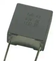
General Purpose Film Capacitor, Metallized PET, Radial Box - 2 Pin, 0.22 µF, ± 10%, 63 V, 100 V
- Manufacturer: VISHAY
- Product type: General Purpose Film Capacitors
- SVHC: No SVHC (04-Feb-2026)
- Capacitance: 0.22µF
- Voltage(AC): 63V
- Voltage(DC): 100V
- Lead Spacing: 7.62mm
- Product Range: MKT371 Series
- Product Width: 4mm
- Qualification: -
- Product Height: 9mm
- Product Length: 10mm
- Dielectric Type: Metallized PET
- Humidity Rating: GRADE II (Test Condition A)
- Capacitor Mounting: Through Hole
- Capacitor Terminals: PC Pin
- Capacitance Tolerance: ± 10%
- Capacitor Case / Package: Radial Box - 2 Pin
- Operating Temperature Max: 105°C
- Operating Temperature Min: -55°C
| Delivery and price | |
|---|---|
| Units per pack | 1000 |
| Price | 0.539 € |
| Current stock | 10+ |
| Lead time | 30 days |
**MKT366, MKT367**

Vishay BCcomponents

www.vishay.com

## **DC Film Capacitor MKT Radial Lacquered Type**

**==> picture [239 x 119] intentionally omitted <==**

## **FEATURES**

- Available taped and loose in box

- Material categorization: for definitions of compliance please see www.vishay.com/doc?99912

## **APPLICATIONS**

Blocking and coupling, bypass and energy reservoir.

## **QUICK REFERENCE DATA**

|**QUICK REFERENCE DATA**|**QUICK REFERENCE DATA**|**QUICK REFERENCE DATA**|**QUICK REFERENCE DATA**|
|---|---|---|---|
|Capacitance range (E12 series)|||**366:**0.0033 μF to 1.0 μF<br>**367:**0.0033μF to 1.0μF|
|Capacitance tolerance|||± 10 %, ± 5 %|
|Climatic testingclass accordingto IEC 60068-1|||55/105/56|
|Maximum application temperature|||105 °C|
|Reference specifications|||IEC 60384-2|
|Dielectric|||Polyester film|
|Electrodes|||Metallized|
|Construction|||Mono construction|
|||||
|Encapsulation|Flame retardant epoxymaterial UL-class 94 V-0|||
|Leads|Tinned wire|||
|Marking|C-value; rated voltage; tolerance|||
|Rated temperature|85 °C|||
|Rated(DC)voltage|63 VDC, 100 VDC, 250 VDC, 400 VDC|||
|Rated(AC)voltage|40 VAC, 63 VAC, 160 VAC, 220 VAC|||


## **Note**

- For more detailed data and test requirements, contact dc-film@vishay.com

## **DIMENSIONS** in millimeters

**==> picture [506 x 157] intentionally omitted <==**

**----- Start of picture text -----**<br>
MKT366 KINKED LEADS MKT367 STRAIGHT LEADS<br>l w l w<br>Seating h Seating h<br>plane  [(1)]<br>plane  [(1)]<br>�<br>� 1.5<br>(2)<br>lt P [+ 0.4] - 0.2 lt<br>P [+ 0.4] - 0.2 Ø 1.3<br>A [(3)] Ø dt Ø dt<br>**----- End of picture text -----**<br>


## **Notes**

- (1) Hole Ø 1.0 for dt = 0.5 mm

- (2) 0 ≤ α < 50°

- (3) A = 1.7 mm ± 0.3 mm

Revision: 07-Nov-2022

Document Number: 28102

**1**

For technical questions, contact: dc-film@vishay.com THIS DOCUMENT IS SUBJECT TO CHANGE WITHOUT NOTICE. THE PRODUCTS DESCRIBED HEREIN AND THIS DOCUMENT ARE SUBJECT TO SPECIFIC DISCLAIMERS, SET FORTH AT www.vishay.com/doc?91000

**MKT366, MKT367**

**==> picture [77 x 10] intentionally omitted <==**

**----- Start of picture text -----**<br>
www.vishay.com<br>**----- End of picture text -----**<br>


## Vishay BCcomponents

## **COMPOSITION OF CATALOG NUMBER: MKT366**

||**TYPE AND PITCHES**|**TYPE AND PITCHES**|**TYPE AND PITCHES**|**TYPE AND PITCHES**|**TYPE AND PITCHES**|**TYPE AND PITCHES**|**CAPACITANCE**<br>**(numerically)**|**CAPACITANCE**<br>**(numerically)**|**CAPACITANCE**<br>**(numerically)**|**CAPACITANCE**<br>**(numerically)**|**CAPACITANCE**<br>**(numerically)**|**CAPACITANCE**<br>**(numerically)**|**CAPACITANCE**<br>**(numerically)**|**CAPACITANCE**<br>**(numerically)**||||||||||
|---|---|---|---|---|---|---|---|---|---|---|---|---|---|---|---|---|---|---|---|---|---|---|---|
||366|||7.5 mm||||||||||||||||||||
|||||||||||||||||||||||||
|||||||||||||||||||||||||
|||||||||||||||||||||||||
||||||||||||||||Example:<br>104 = 10 x 10 = 100 nF|||||||||
|||||||||||||||||||||||||
|||||BFC2||366||XX|||||||YY||Y|||||||
|||||2222(*)||366||XX|||||||YY||Y|||||||
|||||(*) Old ordering number||||||||||||||||||||
|||||||||||||||||||||||||
||**TYPE**|**PACKAGING**|||**LEAD CONFIGURATION**||||||||||**PREFERRED TYPES**|||||||||
|||||||||||**C-TOL.**|||||**63 V**|||**100 V**||**250 V**|||**400 V**|
|**Pitch = 7.5 m**||**m**||||||||||||||||||||||
|366||Loose in box|||Kinked; Lead length<br>4.0 mm + 1.0 mm /- 0.5 m||||m|± 10 %|||||15|||25||45|||55|
|||||||||||± 5 %|||||16|||26||46|||56|
||||||Kinked; Lead length<br>17.0 mm ± 4.0 mm|||||± 10 %|||||11|||21||41|||51|
|||||||||||± 5 %|||||12|||22||42|||52|
|||Ammopack(1)|||Kinked;<br>H = 16.0 mm; P0= 12.7 m||||m|± 10 %|||||13|||23||43|||53|
|||||||||||± 5 %|||||17|||27||47|||57|
|**Note**<br>•<br>For detailed tape specifications refer to packaging information:|||||||||www.vishay.com/doc?28139|||||||||||||||
|**SPECIFIC REFERENCE DATA: MKT366**||||||||||||||||||||||||
|**DESCRIPTION**|||||||||**VALUE**|||||||||||||||
|Tangent of loss angle:<br>C≤0.47 μF<br>C > 0.47 μF|||||||||at 1 kHz|||||||at 10 kHz|||||at 100 kHz|||
||||||||||≤75 x 10-4<br>≤75 x 10-4|||||||≤130 x 10-4<br>≤130 x 10-4|||||≤225 x 10-4<br>-|||
|Rated voltage pulse slope (dU/dt)Rat|||||||||63 VDC||||100 VDC||||||250 VDC|||400 VDC||
||||||||||110 V/μs||||110 V/μs||||||130 V/μs|||170 V/μs||
|R between leads, for C≤0.33 μF<br>at 10 V; 1 min<br>at 100 V; 1 min|||||||||> 15 000 MΩ||||> 15 000 MΩ||||||> 30 000 MΩ|||> 30 000 MΩ||
|RC between leads, for C > 0.33 μF at 10 V; 1 min|||||||||> 5000 s||||||||||-|||||
|R between interconnectingleads and casing, 100 V; 1 min|||||||||> 30 000 MΩ|||||||||||||||
|Withstanding (DC) voltage (cut off current 10 mA)(1);<br>rise time≤1000 V/s||||||||100 V; 1 min|||||160 V; 1 min||||||400 V; 1 min|||640 V; 1 min||
|Maximum application temperature||||||||105 °C||||||||||||||||


## **Note**

> (1) See “Voltage Proof Test for Metallized Film Capacitors”: www.vishay.com/doc?28169

Revision: 07-Nov-2022

Document Number: 28102

**2**

For technical questions, contact: dc-film@vishay.com THIS DOCUMENT IS SUBJECT TO CHANGE WITHOUT NOTICE. THE PRODUCTS DESCRIBED HEREIN AND THIS DOCUMENT ARE SUBJECT TO SPECIFIC DISCLAIMERS, SET FORTH AT www.vishay.com/doc?91000

**MKT366, MKT367**

www.vishay.com

Vishay BCcomponents

|**ELECTRICAL DATA AND ORDERING INFORMATION: MKT366**|**ELECTRICAL DATA AND ORDERING INFORMATION: MKT366**|**ELECTRICAL DATA AND ORDERING INFORMATION: MKT366**|**ELECTRICAL DATA AND ORDERING INFORMATION: MKT366**|**ELECTRICAL DATA AND ORDERING INFORMATION: MKT366**|**ELECTRICAL DATA AND ORDERING INFORMATION: MKT366**|**ELECTRICAL DATA AND ORDERING INFORMATION: MKT366**|**ELECTRICAL DATA AND ORDERING INFORMATION: MKT366**|**ELECTRICAL DATA AND ORDERING INFORMATION: MKT366**|**ELECTRICAL DATA AND ORDERING INFORMATION: MKT366**|**ELECTRICAL DATA AND ORDERING INFORMATION: MKT366**|
|---|---|---|---|---|---|---|---|---|---|---|
|**URDC**<br>**(V)**|**CAP.**<br>**(μF)**|**DIMENSIONS**<br>**wmax. x hmax. x lmax.**<br>**(mm)**|**MASS**<br>**(g)(1)**|**CATALOG NUMBER BFC2 366 XXYYY AND PACKAGING**|||||||
|||||**LOOSE IN BOX**||||**AMMOPACK**||**C-VALUE**|
|||||**lt = 4.0 mm**<br>**+ 1.0 mm / - 0.5 mm**||**lt = 17.0 mm**<br>**± 4.0 mm**||**H = 16.0 mm**|||
|||||**C-TOL. =**<br>**± 10 %**|**C-TOL. =**<br>**± 5 %**|**C-TOL. =**<br>**± 10 %**|**C-TOL. =**<br>**± 5 %**|**C-TOL. =**<br>**± 10 %**|**C-TOL. =**<br>**± 5 %**||
|||||**XX**<br>**(SPQ)**|**XX**<br>**(SPQ)**|**XX**<br>**(SPQ)**|**XX**<br>**(SPQ)**|**XX**<br>**(SPQ)**|**XX**<br>**(SPQ)**|**..YYY**|
|63|**PITCH = 7.5 mm + 0.4 mm / - 0.2 mm; dt = 0.60 mm ± 0.06 mm (URAC = 40 V)**||||||||||
||0.12<br>0.15<br>0.18<br>0.22|4.0 x 12.0 x 10.0|0.30|**15...**<br>(1000)|**16...**<br>(1000)|**11...**<br>(1000)|**12...**<br>(1000)|**13...**<br>(1500)|**17...**<br>(1500)|**124**<br>**154**<br>**184**<br>**224**|
||0.27|4.5 x 13.0 x 10.5|0.38|**15...**<br>(1000)|**16...**<br>(1000)|**11...**<br>(1000)|**12...**<br>(1000)|**13...**<br>(1250)|**17...**<br>(1250)|**274**|
||0.33<br>0.39|5.0 x 13.5 x 10.5|0.43|**15...**<br>(1000)|**16...**<br>(1000)|**11...**<br>(1000)|**12...**<br>(1000)|**13...**<br>(1000)|**17...**<br>(1000)|**334**<br>**394**|
||0.47|5.5 x 14.0 x 10.5|0.53|**15...**<br>(1000)|**16...**<br>(1000)|**11...**<br>(1000)|**12...**<br>(1000)|**13...**<br>(1000)|**17...**<br>(1000)|**474**|
||0.56<br>0.68<br>0.82<br>1.0|5.5 x 14.5 x 10.5|0.54|**15...**<br>(1000)|**16...**<br>(1000)|**11...**<br>(1000)|**12...**<br>(1000)|**13...**<br>(1000)|**17...**<br>(1000)|**564**<br>**684**<br>**824**<br>**105**|
|100|**PITCH = 7.5 mm + 0.4 mm / - 0.2 mm; dt = 0.60 mm ± 0.06 mm (URAC = 63 V)**||||||||||
||0.039<br>0.047<br>0.056<br>0.068<br>0.082|4.0 x 12.0 x 10.0|0.30|**25...**<br>(1000)|**26...**<br>(1000)|**21...**<br>(1000)|**22...**<br>(1000)|**23...**<br>(1500)|**27...**<br>(1500)|**393**<br>**473**<br>**563**<br>**683**<br>**823**|
||0.10|4.0 x 13.0 x 10.0|0.26|**25...**<br>(1000)|**26...**<br>(1000)|**21...**<br>(1000)|**22...**<br>(1000)|**23...**<br>(1500)|**27...**<br>(1500)|**104**|
||0.12|4.5 x 13.0 x 10.5|0.38|**25...**<br>(1000)|**26...**<br>(1000)|**21...**<br>(1000)|**22...**<br>(1000)|**23...**<br>(1250)|**27...**<br>(1250)|**124**|
||0.15|5.0 x 13.0 x 15.0|0.40|**25...**<br>(1000)|**26...**<br>(1000)|**21...**<br>(1000)|**22...**<br>(1000)|**23...**<br>(1000)|**27...**<br>(1000)|**154**|
||0.18|5.0 x 13.5 x 10.5|0.43|**25...**<br>(1000)|**26...**<br>(1000)|**21...**<br>(1000)|**22...**<br>(1000)|**23...**<br>(1000)|**27...**<br>(1000)|**184**|
||0.22|5.5 x 13.5 x 10.5|0.50|**25...**<br>(1000)|**26...**<br>(1000)|**21...**<br>(1000)|**22...**<br>(1000)|**23...**<br>(1000)|**27...**<br>(1000)|**224**|
||0.27|6.0 x 14.5 x 10.5|0.55|**25...**<br>(1000)|**26...**<br>(1000)|**21...**<br>(1000)|**22...**<br>(1000)|**23...**<br>(1000)|**27...**<br>(1000)|**274**|
||0.33<br>0.39<br>0.47|6.0 x 15.0 x 10.5|0.58|**25...**<br>(1000)|**26...**<br>(1000)|**21...**<br>(1000)|**22...**<br>(1000)|**23...**<br>(1000)|**27...**<br>(1000)|**334**<br>**394**<br>**474**|


## **Notes**

- SPQ = Standard Packing Quantity

- (1) Net weight for short lead products only

Revision: 07-Nov-2022

Document Number: 28102

**3**

For technical questions, contact: dc-film@vishay.com THIS DOCUMENT IS SUBJECT TO CHANGE WITHOUT NOTICE. THE PRODUCTS DESCRIBED HEREIN AND THIS DOCUMENT ARE SUBJECT TO SPECIFIC DISCLAIMERS, SET FORTH AT www.vishay.com/doc?91000

**MKT366, MKT367**

www.vishay.com

Vishay BCcomponents

## **ELECTRICAL DATA AND ORDERING INFORMATION: MKT366**

|**ELECTRICAL DATA AND ORDERING INFORMATION: MKT366**|**ELECTRICAL DATA AND ORDERING INFORMATION: MKT366**|**ELECTRICAL DATA AND ORDERING INFORMATION: MKT366**|**ELECTRICAL DATA AND ORDERING INFORMATION: MKT366**|**ELECTRICAL DATA AND ORDERING INFORMATION: MKT366**|**ELECTRICAL DATA AND ORDERING INFORMATION: MKT366**|**ELECTRICAL DATA AND ORDERING INFORMATION: MKT366**|**ELECTRICAL DATA AND ORDERING INFORMATION: MKT366**|**ELECTRICAL DATA AND ORDERING INFORMATION: MKT366**|**ELECTRICAL DATA AND ORDERING INFORMATION: MKT366**|**ELECTRICAL DATA AND ORDERING INFORMATION: MKT366**|
|---|---|---|---|---|---|---|---|---|---|---|
|**URDC**<br>**(V)**|**CAP.**<br>**(μF)**|**DIMENSIONS**<br>**wmax. x hmax. x lmax.**<br>**(mm)**|**MASS**<br>**(g)(1)**|**CATALOG NUMBER BFC2 366 XXYYY AND PACKAGING**|||||||
|||||**LOOSE IN BOX**||||**AMMOPACK**||**C-VALUE**|
|||||**lt = 4.0 mm**<br>**+ 1.0 mm / - 0.5 mm**||**lt = 17.0 mm**<br>**± 4.0 mm**||**H = 16.0 mm**|||
|||||**C-TOL. =**<br>**± 10 %**|**C-TOL. =**<br>**± 5 %**|**C-TOL. =**<br>**± 10 %**|**C-TOL. =**<br>**± 5 %**|**C-TOL. =**<br>**± 10 %**|**C-TOL. =**<br>**± 5 %**||
|||||**XX**<br>**(SPQ)**|**XX**<br>**(SPQ)**|**XX**<br>**(SPQ)**|**XX**<br>**(SPQ)**|**XX**<br>**(SPQ)**|**XX**<br>**(SPQ)**|**..YYY**|
|250|**PITCH = 7.5 mm + 0.4 mm / - 0.2 mm; dt = 0.60 mm ± 0.06 mm (URAC = 160 V)**||||||||||
||0.018<br>0.022<br>0.027<br>0.033<br>0.039<br>0.047|4.0 x 13.0 x 10.0|0.26|**45...**<br>(1000)|**46...**<br>(1000)|**41...**<br>(1000)|**42...**<br>(1000)|**43...**<br>(1500)|**47...**<br>(1500)|**183**<br>**223**<br>**273**<br>**333**<br>**393**<br>**473**|
||0.056|4.0 x 14.0 x 10.0|0.35|**45...**<br>(1000)|**46...**<br>(1000)|**41...**<br>(1000)|**42...**<br>(1000)|**43...**<br>(1500)|**47...**<br>(1500)|**563**|
||0.068|4.5 x 14.0 x 10.0|0.39|**45...**<br>(1000)|**46...**<br>(1000)|**41...**<br>(1000)|**42...**<br>(1000)|**43...**<br>(1250)|**47...**<br>(1250)|**683**|
||0.082|4.5 x 13.0 x 10.0|0.38|**45...**<br>(1000)|**46...**<br>(1000)|**41...**<br>(1000)|**42...**<br>(1000)|**43...**<br>(1250)|**47...**<br>(1250)|**823**|
||0.10|5.0 x 13.5 x 10.0|0.40|**45...**<br>(1000)|**46...**<br>(1000)|**41...**<br>(1000)|**42...**<br>(1000)|**43...**<br>(1000)|**47...**<br>(1000)|**104**|
||0.12|5.5 x 14.0 x 10.0|0.50|**45...**<br>(1000)|**46...**<br>(1000)|**41...**<br>(1000)|**42...**<br>(1000)|**43...**<br>(1000)|**47...**<br>(1000)|**124**|
||0.15|5.5 x 15.5 x 10.0|0.58|**45...**<br>(1000)|**46...**<br>(1000)|**41...**<br>(1000)|**42...**<br>(1000)|**43...**<br>(1000)|**47...**<br>(1000)|**154**|
|400|**PITCH = 7.5 mm + 0.4 mm / - 0.2 mm; dt = 0.60 mm ± 0.06 mm (URAC = 220 V)**||||||||||
||0.0033<br>0.0039<br>0.0047|4.0 x 12.0 x 10.0|0.30|**55...**<br>(1000)|**56...**<br>(1000)|**51...**<br>(1000)|**52...**<br>(1000)|**53...**<br>(1500)|**57...**<br>(1500)|**332**<br>**392**<br>**472**|
||0.0056<br>0.0068<br>0.0082<br>0.010<br>0.012<br>0.015|4.0 x 13.0 x 10.0|0.26|**55...**<br>(1000)|**56...**<br>(1000)|**51...**<br>(1000)|**52...**<br>(1000)|**53...**<br>(1500)|**57...**<br>(1500)|**562**<br>**682**<br>**822**<br>**103**<br>**123**<br>**153**|
||0.018|4.0 x 13.5 x 10.0|0.35|**55...**<br>(1000)|**56...**<br>(1000)|**51...**<br>(1000)|**52...**<br>(1000)|**53...**<br>(1250)|**57...**<br>(1250)|**183**|
||0.022|5.0 x 14.0 x 10.0|0.45|**55...**<br>(1000)|**56...**<br>(1000)|**51...**<br>(1000)|**52...**<br>(1000)|**53...**<br>(1000)|**57...**<br>(1000)|**223**|
||0.027|4.0 x 12.5 x 10.0|0.35|**55...**<br>(1000)|**56...**<br>(1000)|**51...**<br>(1000)|**52...**<br>(1000)|**53...**<br>(1500)|**57...**<br>(1500)|**273**|
||0.033|4.5 x 13.0 x 10.0|0.38|**55...**<br>(1000)|**56...**<br>(1000)|**51...**<br>(1000)|**52...**<br>(1000)|**53...**<br>(1250)|**57...**<br>(1250)|**333**|
||0.039<br>0.047|5.0 x 13.5 x 10.0|0.40|**55...**<br>(1000)|**56...**<br>(1000)|**51...**<br>(1000)|**52...**<br>(1000)|**53...**<br>(1000)|**57...**<br>(1000)|**393**<br>**473**|
||0.056|5.5 x 14.0 x 10.0|0.50|**55...**<br>(1000)|**56...**<br>(1000)|**51...**<br>(1000)|**52...**<br>(1000)|**53...**<br>(1000)|**57...**<br>(1000)|**563**|


## **Notes**

- SPQ = Standard Packing Quantity

- (1) Net weight for short lead products only

Revision: 07-Nov-2022

Document Number: 28102

**4**

For technical questions, contact: dc-film@vishay.com THIS DOCUMENT IS SUBJECT TO CHANGE WITHOUT NOTICE. THE PRODUCTS DESCRIBED HEREIN AND THIS DOCUMENT ARE SUBJECT TO SPECIFIC DISCLAIMERS, SET FORTH AT www.vishay.com/doc?91000

**MKT366, MKT367**

**==> picture [77 x 10] intentionally omitted <==**

**----- Start of picture text -----**<br>
www.vishay.com<br>**----- End of picture text -----**<br>


## Vishay BCcomponents

## **COMPOSITION OF CATALOG NUMBER: MKT367**

||**TYPE AND PITCHES**|**TYPE AND PITCHES**|**TYPE AND PITCHES**|**TYPE AND PITCHES**|**TYPE AND PITCHES**|**TYPE AND PITCHES**|**CAPACITANCE**<br>**(numerically)**|**CAPACITANCE**<br>**(numerically)**|**CAPACITANCE**<br>**(numerically)**|**CAPACITANCE**<br>**(numerically)**|**CAPACITANCE**<br>**(numerically)**|**CAPACITANCE**<br>**(numerically)**|**CAPACITANCE**<br>**(numerically)**|**CAPACITANCE**<br>**(numerically)**||||||||||
|---|---|---|---|---|---|---|---|---|---|---|---|---|---|---|---|---|---|---|---|---|---|---|---|
||367|||7.5 mm||||||||||||||||||||
|||||||||||||||||||||||||
|||||||||||||||||||||||||
|||||||||||||||||||||||||
||||||||||||||||Example:<br>104 = 10 x 10 = 100 nF|||||||||
|||||||||||||||||||||||||
|||||BFC2||367||XX|||YY||||||Y|||||||
|||||2222(*)||367||XX|||YY||||||Y|||||||
|||||(*) Old ordering number||||||||||||||||||||
||**TYPE**|**PACKAGING**|||**LEAD CONFIGURATION**|||||**PREFERRED TYPES**||||||||||||||
|||||||||||**C-TOL.**||||**63 V**||||**100 V**||**250 V**|||**400 V**|
|**Pitch = 7.5 m**||**m**||||||||||||||||||||||
|367||Loose in box|||Straight; Lead length<br>4.0 mm + 1.0 mm /- 0.5 m||||m|± 10 %||||15||||25||45|||55|
|||||||||||± 5 %||||16||||26||46|||56|
||||||Straight; Lead length<br>22.0 mm ± 4.0 mm|||||± 10 %||||11||||21||41|||51|
|||||||||||± 5 %||||12||||22||42|||52|
|||Ammopack(1)|||Straight;<br>H = 18.5 mm; P0= 12.7 m||||m|± 10 %||||13||||23||43|||53|
|||||||||||± 5 %||||17||||27||47|||57|
|**Note**<br>•<br>For detailed tape specifications refer to packaging information:|||||||||www.vishay.com/doc?28139|||||||||||||||
|**SPECIFIC REFERENCE DATA: MKT367**||||||||||||||||||||||||
|**DESCRIPTION**|||||||||**VALUE**|||||||||||||||
|Tangent of loss angle:<br>C≤0.47 μF<br>C > 0.47 μF|||||||||at 1 kHz|||||||at 10 kHz|||||at 100 kHz|||
||||||||||≤75 x 10-4<br>≤75 x 10-4|||||||≤130 x 10-4<br>≤130 x 10-4|||||≤225 x 10-4<br>-|||
|Rated voltage pulse slope (dU/dt)Rat|||||||||63 VDC||||100 VDC||||||250 VDC|||400 VDC||
||||||||||110 V/μs||||110 V/μs||||||130 V/μs|||170 V/μs||
|R between leads, for C≤0.33 μF<br>at 10 V; 1 min<br>at 100 V; 1 min|||||||||> 15 000 MΩ||||> 15 000 MΩ||||||> 30 000 MΩ|||> 30 000 MΩ||
|RC between leads, for C > 0.33 μF at 10 V; 1 min|||||||||> 5000 s||||||||||-|||||
|R between interconnectingleads and casing, 100 V; 1 min|||||||||> 30 000 MΩ|||||||||||||||
|Withstanding (DC) voltage (cut off current 10 mA)(1);<br>rise time≤1000 V/s||||||||100 V; 1 min|||||160 V; 1 min||||||400 V; 1 min|||640 V; 1 min||
|Maximum application temperature||||||||105 °C||||||||||||||||


## **Note**

> (1) See “Voltage Proof Test for Metallized Film Capacitors”: www.vishay.com/doc?28169

Revision: 07-Nov-2022

Document Number: 28102

**5**

For technical questions, contact: dc-film@vishay.com THIS DOCUMENT IS SUBJECT TO CHANGE WITHOUT NOTICE. THE PRODUCTS DESCRIBED HEREIN AND THIS DOCUMENT ARE SUBJECT TO SPECIFIC DISCLAIMERS, SET FORTH AT www.vishay.com/doc?91000

**MKT366, MKT367**

www.vishay.com

## Vishay BCcomponents

## **ELECTRICAL DATA AND ORDERING INFORMATION: MKT367**

|**ELECTRICAL DATA AND ORDERING INFORMATION: MKT367**|**ELECTRICAL DATA AND ORDERING INFORMATION: MKT367**|**ELECTRICAL DATA AND ORDERING INFORMATION: MKT367**|**ELECTRICAL DATA AND ORDERING INFORMATION: MKT367**|**ELECTRICAL DATA AND ORDERING INFORMATION: MKT367**|**ELECTRICAL DATA AND ORDERING INFORMATION: MKT367**|**ELECTRICAL DATA AND ORDERING INFORMATION: MKT367**|**ELECTRICAL DATA AND ORDERING INFORMATION: MKT367**|**ELECTRICAL DATA AND ORDERING INFORMATION: MKT367**|**ELECTRICAL DATA AND ORDERING INFORMATION: MKT367**|**ELECTRICAL DATA AND ORDERING INFORMATION: MKT367**|
|---|---|---|---|---|---|---|---|---|---|---|
|**URDC**<br>**(V)**|**CAP.**<br>**(μF)**|**DIMENSIONS**<br>**wmax. x hmax. x lmax.**<br>**(mm)**|**MASS**<br>**(g)(1)**|**CATALOG NUMBER BFC2 367 XXYYY AND PACKAGING**|||||||
|||||**LOOSE IN BOX**||||**AMMOPACK**||**C-VALUE**|
|||||**lt = 4.0 mm**<br>**+ 1.0 mm / - 0.5 mm**||**lt = 22.0 mm**<br>**± 4.0 mm**||**H = 18.5 mm**|||
|||||**C-TOL. =**<br>**± 10 %**|**C-TOL. =**<br>**± 5 %**|**C-TOL. =**<br>**± 10 %**|**C-TOL. =**<br>**± 5 %**|**C-TOL. =**<br>**± 10 %**|**C-TOL. =**<br>**± 5 %**||
|||||**XX**<br>**(SPQ)**|**XX**<br>**(SPQ)**|**XX**<br>**(SPQ)**|**XX**<br>**(SPQ)**|**XX**<br>**(SPQ)**|**XX**<br>**(SPQ)**|**..YYY**|
|63|**PITCH = 7.5 mm**|||**+ 0.4 mm / - 0.2 mm; dt = 0.60 mm ± 0.06 mm (URAC = 40 V)**|||||||
||0.12<br>0.15<br>0.18<br>0.22|4.0 x 9.5 x 10.0|0.23|**15...**<br>(1000)|**16...**<br>(1000)|**11...**<br>(1000)|**12...**<br>(1000)|**13...**<br>(1500)|**17...**<br>(1500)|**124**<br>**154**<br>**184**<br>**224**|
||0.27|4.5 x 10.0 x 10.5|0.37|**15...**<br>(1000)|**16...**<br>(1000)|**11...**<br>(1000)|**12...**<br>(1000)|**13...**<br>(1000)|**17...**<br>(1000)|**274**|
||0.33<br>0.39|5.0 x 10.5 x 10.5|0.39|**15...**<br>(1000)|**16...**<br>(1000)|**11...**<br>(1000)|**12...**<br>(1000)|**13...**<br>(1000)|**17...**<br>(1000)|**334**<br>**394**|
||0.47|5.5 x 11.0 x 10.5|0.44|**15...**<br>(1000)|**16...**<br>(1000)|**11...**<br>(1000)|**12...**<br>(1000)|**13...**<br>(1000)|**17...**<br>(1000)|**474**|
||0.56<br>0.68<br>0.82<br>1.0|5.5 x 12.0 x 10.5|0.46|**15...**<br>(1000)|**16...**<br>(1000)|**11...**<br>(1000)|**12...**<br>(1000)|**13...**<br>(1000)|**17...**<br>(1000)|**564**<br>**684**<br>**824**<br>**105**|
|100|**PITCH = 7.5 mm**|||**+ 0.4 mm / - 0.2 mm; dt = 0.60 mm ± 0.06 mm (URAC = 63 V)**|||||||
||0.039<br>0.047<br>0.056<br>0.068<br>0.082<br>0.10|4.0 x 9.5 x 10.0|0.23|**25...**<br>(1000)|**26...**<br>(1000)|**21...**<br>(1000)|**22...**<br>(1000)|**23...**<br>(1500)|**27...**<br>(1500)|**393**<br>**473**<br>**563**<br>**683**<br>**823**<br>**104**|
||0.12|4.5 x 10.0 x 10.5|0.37|**25...**<br>(1000)|**26...**<br>(1000)|**21...**<br>(1000)|**22...**<br>(1000)|**23...**<br>(1000)|**27...**<br>(1000)|**124**|
||0.15<br>0.18|5.0 x 10.5 x 10.5|0.39|**25...**<br>(1000)|**26...**<br>(1000)|**21...**<br>(1000)|**22...**<br>(1000)|**23...**<br>(1000)|**27...**<br>(1000)|**154**<br>**184**|
||0.22|5.5 x 11.5 x 10.5|0.44|**25...**<br>(1000)|**26...**<br>(1000)|**21...**<br>(1000)|**22...**<br>(1000)|**23...**<br>(1000)|**27...**<br>(1000)|**224**|
||0.27<br>0.33<br>0.39<br>0.47|6.0 x 12.5 x 10.5|0.55|**25...**<br>(1000)|**26...**<br>(1000)|**21...**<br>(1000)|**22...**<br>(1000)|**23...**<br>(1000)|**27...**<br>(1000)|**274**<br>**334**<br>**394**<br>**474**|


## **Notes**

- SPQ = Standard Packing Quantity

- (1) Net weight for short lead products only

Revision: 07-Nov-2022

Document Number: 28102

**6**

For technical questions, contact: dc-film@vishay.com THIS DOCUMENT IS SUBJECT TO CHANGE WITHOUT NOTICE. THE PRODUCTS DESCRIBED HEREIN AND THIS DOCUMENT ARE SUBJECT TO SPECIFIC DISCLAIMERS, SET FORTH AT www.vishay.com/doc?91000

**MKT366, MKT367**

www.vishay.com

Vishay BCcomponents

## **ELECTRICAL DATA AND ORDERING INFORMATION: MKT367**

|**ELECTRICAL DATA AND ORDERING INFORMATION: MKT367**|**ELECTRICAL DATA AND ORDERING INFORMATION: MKT367**|**ELECTRICAL DATA AND ORDERING INFORMATION: MKT367**|**ELECTRICAL DATA AND ORDERING INFORMATION: MKT367**|**ELECTRICAL DATA AND ORDERING INFORMATION: MKT367**|**ELECTRICAL DATA AND ORDERING INFORMATION: MKT367**|**ELECTRICAL DATA AND ORDERING INFORMATION: MKT367**|**ELECTRICAL DATA AND ORDERING INFORMATION: MKT367**|**ELECTRICAL DATA AND ORDERING INFORMATION: MKT367**|**ELECTRICAL DATA AND ORDERING INFORMATION: MKT367**|**ELECTRICAL DATA AND ORDERING INFORMATION: MKT367**|
|---|---|---|---|---|---|---|---|---|---|---|
|**URDC**<br>**(V)**|**CAP.**<br>**(μF)**|**DIMENSIONS**<br>**wmax. x hmax. x lmax.**<br>**(mm)**|**MASS**<br>**(g)(1)**|**CATALOG NUMBER BFC2 367 XXYYY AND PACKAGING**|||||||
|||||**LOOSE IN BOX**||||**AMMOPACK**||**C-VALUE**|
|||||**lt = 4.0 mm**<br>**+ 1.0 mm / - 0.5 mm**||**lt = 22.0 mm**<br>**± 4.0 mm**||**H = 18.5 mm**|||
|||||**C-TOL. =**<br>**± 10 %**|**C-TOL. =**<br>**± 5 %**|**C-TOL. =**<br>**± 10 %**|**C-TOL. =**<br>**± 5 %**|**C-TOL. =**<br>**± 10 %**|**C-TOL. =**<br>**± 5 %**||
|||||**XX**<br>**(SPQ)**|**XX**<br>**(SPQ)**|**XX**<br>**(SPQ)**|**XX**<br>**(SPQ)**|**XX**<br>**(SPQ)**|**XX**<br>**(SPQ)**|**..YYY**|
|250|**PITCH = 7.5 mm**|||**+ 0.4 mm / - 0.2 mm; dt = 0.60 mm ± 0.06 mm (URAC = 160 V)**|||||||
||0.018<br>0.022<br>0.027<br>0.033<br>0.039<br>0.047<br>0.056|4.0 x 9.5 x 10.0|0.23|**45...**<br>(1000)|**46...**<br>(1000)|**41...**<br>(1000)|**42...**<br>(1000)|**43...**<br>(1500)|**47...**<br>(1500)|**183**<br>**223**<br>**273**<br>**333**<br>**393**<br>**473**<br>**563**|
||0.068<br>0.082|4.5 x 10.0 x 10.0|0.37|**45...**<br>(1000)|**46...**<br>(1000)|**41...**<br>(1000)|**42...**<br>(1000)|**43...**<br>(1000)|**47...**<br>(1000)|**683**<br>**823**|
||0.10|5.0 x 10.5 x 10.0|0.39|**45...**<br>(1000)|**46...**<br>(1000)|**41...**<br>(1000)|**42...**<br>(1000)|**43...**<br>(1000)|**47...**<br>(1000)|**104**|
||0.12|5.5 x 11.0 x 10.0|0.42|**45...**<br>(1000)|**46...**<br>(1000)|**41...**<br>(1000)|**42...**<br>(1000)|**43...**<br>(1000)|**47...**<br>(1000)|**124**|
||0.15|5.5 x 12.5 x 10.0|0.48|**45...**<br>(1000)|**46...**<br>(1000)|**41...**<br>(1000)|**42...**<br>(1000)|**43...**<br>(1000)|**47...**<br>(1000)|**154**|
|400|**PITCH = 7.5 mm**|||**+ 0.4 mm / - 0.2 mm; dt = 0.60 mm ± 0.06 mm (URAC = 220 V)**|||||||
||0.0033<br>0.0039<br>0.0047<br>0.0056<br>0.0068<br>0.0082<br>0.010<br>0.012<br>0.015|4.0 x 9.5 x 10.0|0.23|**55...**<br>(1000)|**56...**<br>(1000)|**51...**<br>(1000)|**52...**<br>(1000)|**53...**<br>(1500)|**57...**<br>(1500)|**332**<br>**392**<br>**472**<br>**562**<br>**682**<br>**822**<br>**103**<br>**123**<br>**153**|
||0.018|4.5 x 10.0 x 10.0|0.37|**55...**<br>(1000)|**56...**<br>(1000)|**51...**<br>(1000)|**52...**<br>(1000)|**53...**<br>(1000)|**57...**<br>(1000)|**183**|
||0.022|5.0 x 10.5 x 10.0|0.39|**55...**<br>(1000)|**56...**<br>(1000)|**51...**<br>(1000)|**52...**<br>(1000)|**53...**<br>(1000)|**57...**<br>(1000)|**223**|
||0.027|4.0 x 9.5 x 10.0|0.23|**55...**<br>(1000)|**56...**<br>(1000)|**51...**<br>(1000)|**52...**<br>(1000)|**53...**<br>(1500)|**57...**<br>(1500)|**273**|
||0.033|4.5 x 10.0 x 10.0|0.37|**55...**<br>(1000)|**56...**<br>(1000)|**51...**<br>(1000)|**52...**<br>(1000)|**53...**<br>(1000)|**57...**<br>(1000)|**333**|
||0.039<br>0.047|5.0 x 10.5 x 10.0|0.39|**55...**<br>(1000)|**56...**<br>(1000)|**51...**<br>(1000)|**52...**<br>(1000)|**53...**<br>(1000)|**57...**<br>(1000)|**393**<br>**473**|
||0.056|5.5 x 11.0 x 10.0|0.42|**55...**<br>(1000)|**56...**<br>(1000)|**51...**<br>(1000)|**52...**<br>(1000)|**53...**<br>(1000)|**57...**<br>(1000)|**563**|


## **Notes**

- SPQ = Standard Packing Quantity

- (1) Net weight for short lead products only

Revision: 07-Nov-2022

Document Number: 28102

**7**

For technical questions, contact: dc-film@vishay.com THIS DOCUMENT IS SUBJECT TO CHANGE WITHOUT NOTICE. THE PRODUCTS DESCRIBED HEREIN AND THIS DOCUMENT ARE SUBJECT TO SPECIFIC DISCLAIMERS, SET FORTH AT www.vishay.com/doc?91000

**MKT366, MKT367** Vishay BCcomponents

www.vishay.com

## **MOUNTING**

## **Normal Use**

The capacitors are designed for mounting on printed-circuit boards. The capacitors packed in bandoliers are designed for mounting in printed-circuit boards by means of automatic insertion machines.

For detailed tape specifications refer to packaging information: www.vishay.com/doc?28139

## **Specific Method of Mounting to Withstand Vibration and Shock**

In order to withstand vibration and shock tests, it must be ensured that the underside and the kinks are in good contact with the printed-circuit board.

- For pitches ≤ 15 mm capacitors shall be mechanically fixed by the leads

- For larger pitches the capacitors shall be mounted in the same way and the body clamped

## **SOLDERING CONDITIONS**

For general soldering conditions and wave soldering profile, we refer to the application note:

“ **Soldering Guidelines for Film Capacitors** ”: www.vishay.com/doc?28171

## **Storage Temperature**

Tstg = -25 °C to +35 °C with RH maximum 75 % without condensation

## **Ratings and Characteristics Reference Conditions**

Unless otherwise specified, all electrical values apply to an ambient free air temperature of 23 °C ± 1 °C, an atmospheric pressure of 86 kPa to 106 kPa and a relative humidity of 50 % ± 2 %.

For reference testing, a conditioning period shall be applied over 96 h ± 4 h by heating the products in a circulating air oven at the rated temperature and a relative humidity not exceeding 20 %.

Revision: 07-Nov-2022

Document Number: 28102

**8** For technical questions, contact: dc-film@vishay.com THIS DOCUMENT IS SUBJECT TO CHANGE WITHOUT NOTICE. THE PRODUCTS DESCRIBED HEREIN AND THIS DOCUMENT ARE SUBJECT TO SPECIFIC DISCLAIMERS, SET FORTH AT www.vishay.com/doc?91000

**MKT366, MKT367** Vishay BCcomponents

> www.vishay.com Vishay BCcomponents a ~~a~~

## **CHARACTERISTICS**

**==> picture [230 x 157] intentionally omitted <==**

**----- Start of picture text -----**<br>
21 Ecce)<br>CCI<br>0 =SEE—CTTono<br>COTTON<br>-1<br>-2<br>-3<br>10 CCIE [2] 10 [3]  CCTs 10 [4] f (Hz) N 10 [5]<br>C/CΔ   (%)<br>**----- End of picture text -----**<br>


Capacitance as a function of frequency (typical curve)

**==> picture [226 x 186] intentionally omitted <==**

**----- Start of picture text -----**<br>
6<br>1 kHz<br>4<br>EEREag<br>2<br>S aC ee eeeeeD////7//CEeEE ee<br>| MIU<br>max.<br>0 OL LY<br>typical<br>-2<br>-4<br>min.<br>-6<br>-60 WAL 4 Yl [Ceeeree] ‘ -20 20 eer 60 Tamb 2  (°C) e Yy 100 d<br>Capacitance as a function of ambient temperature<br>(typical curve)<br>C/CΔ (%)<br>**----- End of picture text -----**<br>


**==> picture [228 x 382] intentionally omitted <==**

**----- Start of picture text -----**<br>
10 [2]<br>SJE 0|<br>10 [0]<br>10 [-1]<br>10 [-2]<br>10 [-3]<br>10 [4] 10 [5] 10 [6] 10 [7] f (Hz) 10 [8]<br>Impedance as a function of frequency<br>(typical curve)<br>10 [2]<br>=F EHH RERR Ht<br>CE CTT<br>10 [1] TMC<br>CMS")<br>ICME Tamb ≤ 85 °C, 63 VDC<br>10 [0]<br>10 perereraera [1] 10 [2] o|( 10 [3] 10 [4] f (Hz) 10 [5]<br>Max. RMS voltage as a function of frequency<br>63 V; 100 nF<br>63 V; 1 µF<br>220 nF<br>470 nF<br>47 nF<br> (1/2)<br>Impedance<br>(V)<br>AC Voltage<br>**----- End of picture text -----**<br>


**==> picture [237 x 177] intentionally omitted <==**

**----- Start of picture text -----**<br>
1.2<br>1.0<br>0.8<br>0.6<br>0.4<br>0.2<br>0.0<br>-60                    -20                     20                      60                     100    Tamb (°C)<br>Max. DC and AC voltage as a function of temperature<br>Factor<br>**----- End of picture text -----**<br>


**==> picture [227 x 176] intentionally omitted <==**

**----- Start of picture text -----**<br>
10 [2]<br>HEHEHE HHH<br>NT<br>10 [1] |<br>COMICS<br>CCHF 85 °C < Tamb ≤ 105 °C, 63 VDC<br>10 [0]<br>10 prrreremreerreran [1] 10 [2] 10 [3] 11 10 [4] S f (Hz) S S 10 [5]<br>Max. RMS voltage as a function of frequency<br>220 nF<br>470 nF<br>47 nF<br>(V)<br>AC Voltage<br>**----- End of picture text -----**<br>


Revision: 07-Nov-2022

Document Number: 28102

**9** For technical questions, contact: dc-film@vishay.com THIS DOCUMENT IS SUBJECT TO CHANGE WITHOUT NOTICE. THE PRODUCTS DESCRIBED HEREIN AND THIS DOCUMENT ARE SUBJECT TO SPECIFIC DISCLAIMERS, SET FORTH AT www.vishay.com/doc?91000

**MKT366, MKT367**

www.vishay.com

Vishay BCcomponents

**==> picture [227 x 177] intentionally omitted <==**

**----- Start of picture text -----**<br>
10 [2]<br>10 [1]<br>Tamb ≤ 85 °C, 100 VDC<br>10 [0]<br>10 [1] 10 [2] 10 [3] 10 [4] f (Hz) 10 [5]<br>Max. RMS voltage as a function of frequency<br>100 nF<br>470 nF<br>10 nF<br>47 nF<br>(V)<br>AC Voltage<br>**----- End of picture text -----**<br>


**==> picture [229 x 159] intentionally omitted <==**

**----- Start of picture text -----**<br>
10 [3]<br>10 [2]<br>10 [1]<br>Tamb ≤ 85 °C, 250 VDC<br>10 [0]<br>10 [1]     10 [2]          10 [3]               10            f (Hz) [4]                10 [5]<br>18 nF<br>47 nF<br>100 nF<br>150 nF<br>(V)<br>AC Voltage<br>**----- End of picture text -----**<br>


Max. RMS voltage as a function of frequency

**==> picture [230 x 176] intentionally omitted <==**

**----- Start of picture text -----**<br>
10 [3]<br>10 [2]<br>10 [1]<br>Tamb ≤ 85 °C, 400 VDC<br>10 [0]<br>10 [1] 10 [2] 10 [3] 10 [4] f (Hz) 10 [5]<br>Max. RMS voltage as a function of frequency<br>3.3 nF<br>15 nF<br>33 nF<br>56 nF<br>(V)<br>AC Voltage<br>**----- End of picture text -----**<br>


**==> picture [227 x 177] intentionally omitted <==**

**----- Start of picture text -----**<br>
10 [2]<br>10 [1]<br>85 °C < Tamb ≤ 105 °C, 100 VDC<br>10 [0]<br>10 [1] 10 [2] 10 [3] 10 [4] f (Hz) 10 [5]<br>Max. RMS voltage as a function of frequency<br>100 nF<br>470 nF<br>10 nF<br>47 nF<br>(V)<br>AC Voltage<br>**----- End of picture text -----**<br>


**==> picture [229 x 176] intentionally omitted <==**

**----- Start of picture text -----**<br>
10 [3]<br>10 [2]<br>10 [1]<br>85 °C < Tamb ≤ 105 °C, 250 VDC<br>10 [0]<br>10 [1] 10 [2] 10 [3] 10 [4] f (Hz) 10 [5]<br>Max. RMS voltage as a function of frequency<br>18 nF<br>47 nF<br>100 nF<br>150 nF<br>(V)<br>AC Voltage<br>**----- End of picture text -----**<br>


**==> picture [229 x 176] intentionally omitted <==**

**----- Start of picture text -----**<br>
10 [3]<br>10 [2]<br>10 [1]<br>85 °C < Tamb ≤ 105 °C, 400 VDC<br>10 [0]<br>10 [1] 10 [2] 10 [3] 10 [4] f (Hz) 10 [5]<br>Max. RMS voltage as a function of frequency<br>3.3 nF<br>15 nF<br>33 nF<br>56 nF<br>(V)<br>AC Voltage<br>**----- End of picture text -----**<br>


Revision: 07-Nov-2022

Document Number: 28102

**10** For technical questions, contact: dc-film@vishay.com THIS DOCUMENT IS SUBJECT TO CHANGE WITHOUT NOTICE. THE PRODUCTS DESCRIBED HEREIN AND THIS DOCUMENT ARE SUBJECT TO SPECIFIC DISCLAIMERS, SET FORTH AT www.vishay.com/doc?91000

**MKT366, MKT367**

www.vishay.com

Vishay BCcomponents

## **MAXIMUM RMS CURRENT (SINEWAVE) AS A FUNCTION OF FREQUENCY**

## The maximum RMS current is defined by IAC = ω x C x UAC

UAC is the maximum AC voltage depending on the ambient temperature in the curves “Max. RMS voltage and AC current as a function of frequency”.

**==> picture [493 x 186] intentionally omitted <==**

**----- Start of picture text -----**<br>
10 [3] 10 [5]<br>5<br>4<br>3 10 [4]<br>2<br>1<br>10 [2]<br>Curve 1: C = 0.33 µF 10 [3]<br>Curve 2: 0.33 µF, C = 1.2 µF<br>Curve 3: 1.2 µF, C = 3.9 µF<br>Curve 4: 3.9 µF, C = 6.8 µF<br>Curve 5: C = 6.8 µF<br>10 [1] 10 [2]<br>10 [2] 10 [3] 10 [4] f (Hz) 10 [5] -50    0   50 Tamb (°C) 100<br>Tangent of loss angle as a function of frequency Insulation resistance as a function of the<br>ambient temperature (typical curve)<br>-4) RC (s)<br>(x 10<br>Dissipation factor<br>**----- End of picture text -----**<br>


**==> picture [221 x 187] intentionally omitted <==**

**----- Start of picture text -----**<br>
16<br>12<br>  8<br>  4<br>  0<br>-60                  -20                    20                     60                   100    Tamb (°C)<br>Maximum allowed component temperature rise (ΔT)<br>as a function of the ambient temperature (Tamb)<br>T (°C)<br>Δ<br>**----- End of picture text -----**<br>


## **HEAT CONDUCTIVITY (G) AS A FUNCTION OF (ORIGINAL) PITCH AND CAPACITOR BODY THICKNESS IN mW/°C**

|**HEAT CONDUCTIVITY (G) AS A FUNCTION OF (ORIGINAL) PITCH AND CAPACITOR BODY**<br>**THICKNESS IN mW/°C**|**HEAT CONDUCTIVITY (G) AS A FUNCTION OF (ORIGINAL) PITCH AND CAPACITOR BODY**<br>**THICKNESS IN mW/°C**|
|---|---|
|**Wmax.**<br>**(mm)**|**HEAT CONDUCTIVITY**<br>**(mW/°C)**|
|3.5|3.0|
|4.0|3.5|
|4.5|3.5|
|5.0|4.0|
|5.5|4.0|
|6.0|4.5|
|6.5|5.0|


Revision: 07-Nov-2022

Document Number: 28102

**11**

For technical questions, contact: dc-film@vishay.com THIS DOCUMENT IS SUBJECT TO CHANGE WITHOUT NOTICE. THE PRODUCTS DESCRIBED HEREIN AND THIS DOCUMENT ARE SUBJECT TO SPECIFIC DISCLAIMERS, SET FORTH AT www.vishay.com/doc?91000

**MKT366, MKT367**

www.vishay.com

Vishay BCcomponents

## **POWER DISSIPATION AND MAXIMUM COMPONENT TEMPERATURE RISE**

The power dissipation must be limited in order not to exceed the maximum allowed component temperature rise as a function of the free ambient temperature.

The power dissipation can be calculated according type detail specification “HQN-384-01/101: Technical Information Film Capacitors”.

The component temperature rise (ΔT) can be measured (see section “Measuring the Component Temperature” for more details) or calculated by ΔT = P/G:

- ΔT = component temperature rise (°C)

- P = power dissipation of the component (mW)

- G = heat conductivity of the component (mW/°C)

## **MEASURING THE COMPONENT TEMPERATURE**

A thermocouple must be attached to the capacitor body as in:

**==> picture [46 x 8] intentionally omitted <==**

**----- Start of picture text -----**<br>
Thermocouple<br>**----- End of picture text -----**<br>


The temperature is measured in unloaded (Tamb) and maximum loaded condition (TC).

The temperature rise is given by ΔT = TC - Tamb.

To avoid radiation or convection, the capacitor should be tested in a wind-free box.

## **APPLICATION NOTE AND LIMITING CONDITIONS**

These capacitors are not suitable for mains applications as across-the-line capacitors without additional protection, as described hereunder. These mains applications are strictly regulated in safety standards and therefore electromagnetic interference suppression capacitors conforming the standards must be used.

To select the capacitor for a certain application, the following conditions must be checked:

1. For capacitors connected in parallel, normally the proof voltage and possibly the rated voltage must be reduced. For information depending of the capacitance value and the number of parallel connections contact: dc-film@vishay.com

2. The peak voltage (UP) shall not be greater than the rated DC voltage (URDC)

3. The peak-to-peak voltage (UP-P) shall not be greater than 2√2 x URAC to avoid the ionization inception level

4. The voltage pulse slope (dU/dt) shall not exceed the rated voltage pulse slope in an RC-circuit at rated voltage and without ringing. If the pulse voltage is lower than the rated DC voltage, the rated voltage pulse slope may be multiplied by URDC and divided by the applied voltage.

For all other pulses following equation must be fulfilled:

**==> picture [144 x 35] intentionally omitted <==**

T is the pulse duration.

The rated voltage pulse slope is valid for ambient temperatures up to 85 °C. For higher temperatures a derating factor of 3 % per K shall be applied.

Revision: 07-Nov-2022

Document Number: 28102

**12**

For technical questions, contact: dc-film@vishay.com THIS DOCUMENT IS SUBJECT TO CHANGE WITHOUT NOTICE. THE PRODUCTS DESCRIBED HEREIN AND THIS DOCUMENT ARE SUBJECT TO SPECIFIC DISCLAIMERS, SET FORTH AT www.vishay.com/doc?91000

**MKT366, MKT367**

Vishay BCcomponents

www.vishay.com

5. The maximum component surface temperature rise must be lower than the limits (see graph “Max. allowed component temperature rise”).

6. Since in circuits used at voltages over 280 V peak-to-peak the risk for an intrinsically active flammability after a capacitor breakdown (short circuit) increases, it is recommended that the power to the component is limited to 100 times the values mentioned in the table: “Heat Conductivity”

7. When using these capacitors as across-the-line capacitor in the input filter for mains applications or as series connected with an impedance to the mains the applicant must guarantee that the following conditions are fulfilled in any case (spikes and surge voltages from the mains included).

|**VOLTAGE CONDITIONS FOR 6 ABOVE**|**VOLTAGE CONDITIONS FOR 6 ABOVE**|**VOLTAGE CONDITIONS FOR 6 ABOVE**|
|---|---|---|
|**ALLOWED VOLTAGES**|**Tamb **≤**85 °C**|**85 °C < Tamb **≤**105 °C**|
|Maximum continuous RMS voltage|URAC|0.8 x URAC|
|Maximum temperature RMS-overvoltage (< 24 h)|1.25 x URAC|URAC|
|Maximum peak voltage (VO-P) (< 2 s)|1.6 x URDC|1.3 x URDC|


## **Example**

C = 330 nF - 63 V used for the voltage signal shown in next drawing. UP-P = 40 V; UP = 35 V; T1 = 100 μs; T2 = 200 μs

The ambient temperature is 35 °C

Checking conditions:

1. The peak voltage UP = 35 V is lower than 63 VDC

2. The peak-to-peak voltage 40 V is lower than 2√2 x 40 VAC = 113 UP-P

3. The voltage pulse slope (dU/dt) = 40 V/100 μs = 0.4 V/μs This is lower than 110 V/μs (see specific reference data for each version)

4. The dissipated power is 16.2 mW as calculated with fourier terms

The temperature rise for Wmax. = 4.5 mm and pitch = 5 mm will be 16.2 mW/2.5 mW/°C = 6.5 °C

   - This is lower than 15 °C temperature rise at 35 °C, according figure “Max. allowed component temperature rise”

5. Not applicable

6. Not applicable

## **Voltage Signal**

**==> picture [310 x 136] intentionally omitted <==**

**----- Start of picture text -----**<br>
Voltage<br>UP<br>UP-P<br>Time<br>T1<br>T2<br>**----- End of picture text -----**<br>


Revision: 07-Nov-2022

Document Number: 28102

**13** For technical questions, contact: dc-film@vishay.com THIS DOCUMENT IS SUBJECT TO CHANGE WITHOUT NOTICE. THE PRODUCTS DESCRIBED HEREIN AND THIS DOCUMENT ARE SUBJECT TO SPECIFIC DISCLAIMERS, SET FORTH AT www.vishay.com/doc?91000

**MKT366, MKT367** Vishay BCcomponents

www.vishay.com

## **INSPECTION REQUIREMENTS**

## **General Notes**

Sub-clause numbers of tests and performance requirements refer to the “Sectional Specification, Publication IEC 60384-2 and Specific Reference Data”.

|**GROUP C INSPECTION REQUIREMENTS**|**GROUP C INSPECTION REQUIREMENTS**|**GROUP C INSPECTION REQUIREMENTS**|
|---|---|---|
|**SUB-CLAUSE NUMBER AND TEST**|**CONDITIONS**|**PERFORMANCE REQUIREMENTS**|
|**SUB-GROUP C1A PART OF SAMPLE**<br>**OF SUB-GROUP C1**|||
|4.1<br>Dimensions (detail)<br>4.3.1 Initial measurements<br>4.3<br>Robustness of terminations<br>4.4<br>Resistance to soldering heat<br>4.14 Component solvent resistance<br>4.4.2 Final measurements|Capacitance<br>Tangent of loss angle:<br>for C≤470 nF at 100 kHz or<br>for C > 470 nF at 10 kHz<br>Tensile: load 10 N; 10 s<br>Bending: load 5 N; 4 x 90°<br>Method: 1A<br>Solder bath: 280 °C ± 5 °C<br>Duration: 10 s<br>Isopropylalcohol at room temperature<br>Method: 2<br>Immersion time: 5 min ± 0.5 min<br>Recovery time: min. 1 h, max. 2 h<br>Visual examination<br>Capacitance<br>Tangent of loss angle|As specified in chapters “General Data” of<br>this specification<br>No visible damage<br>No visible damage<br>Legible marking<br>|ΔC/C|≤2 % of the value measured initially<br>Increase of tanδ<br>≤0.005 for: C≤100 nF or<br>≤0.010 for: 100 nF < C≤220 nF or<br>≤0.015 for: 220 nF < C≤470 nF and<br>≤0.003 for: C > 470 nF<br>Compared to values measured in 4.3.1|
|**SUB-GROUP C1B PART OF SAMPLE**<br>**OF SUB-GROUP C1**|||
|4.6.1 Initial measurements<br>4.6<br>Rapid change of temperature<br>4.7<br>Vibration<br>4.7.2 Final inspection|Capacitance<br>Tangent of loss angle:<br>for C≤470 nF at 100 kHz or<br>for C > 470 nF at 10 kHz<br>θA = -55 °C<br>θB = +105 °C<br>5 cycles<br>Duration t = 30 min<br>Visual examination<br>Mounting:<br>See section “Mounting” of this specification<br>Procedure B4<br>Frequency range: 10 Hz to 55 Hz<br>Amplitude: 0.75 mm or<br>Acceleration 98 m/s2<br>(whichever is less severe)<br>Total duration 6 h<br>Visual examination|No visible damage<br>No visible damage<br>No visible damage|


Revision: 07-Nov-2022

Document Number: 28102

**14**

For technical questions, contact: dc-film@vishay.com THIS DOCUMENT IS SUBJECT TO CHANGE WITHOUT NOTICE. THE PRODUCTS DESCRIBED HEREIN AND THIS DOCUMENT ARE SUBJECT TO SPECIFIC DISCLAIMERS, SET FORTH AT www.vishay.com/doc?91000

**MKT366, MKT367**

www.vishay.com

Vishay BCcomponents

## **GROUP C INSPECTION REQUIREMENTS**

|**GROUP C INSPECTION REQUIREMENTS**|**GROUP C INSPECTION REQUIREMENTS**|**GROUP C INSPECTION REQUIREMENTS**|
|---|---|---|
|**SUB-CLAUSE NUMBER AND TEST**|**CONDITIONS**|**PERFORMANCE REQUIREMENTS**|
|**SUB-GROUP C1B PART OF SAMPLE**<br>**OF SUB-GROUP C1**|||
|4.9<br>Shock<br>4.9.3<br>Final measurements|Mounting:<br>See section “Mounting” of this specification<br>Pulse shape: half sine<br>Acceleration: 490 m/s2<br>Duration of pulse: 11 ms<br>Visual examination<br>Capacitance<br>Tangent of loss angle<br>Insulation resistance|No visible damage<br>|ΔC/C|≤3 % of the value measured in 4.6.1<br>Increase of tanδ<br>≤0.005 for: C≤100 nF or<br>≤0.010 for: 100 nF < C≤220 nF or<br>≤0.015 for: 220 nF < C≤470 nF and<br>≤0.003 for: C > 470 nF<br>Compared to values measured in 4.6.1<br>As specified in section “Insulation<br>Resistance” of this specification|
|**SUB-GROUP C1 COMBINED SAMPLE**<br>**OF SPECIMENS OF SUB-GROUPS**<br>**C1A AND C1B**|||
|4.10<br>Climatic sequence<br>4.10.2<br>Dry heat<br>4.10.3<br>Damp heat cyclic<br>Test Db, first cycle<br>4.10.4<br>Cold<br>4.10.6<br>Damp heat cyclic<br>Test Db, remaining cycles<br>4.10.6.2<br>Final measurements|Temperature: +105 °C<br>Duration: 16 h<br>Temperature: -55 °C<br>Duration: 2 h<br>Voltage proof = URDCfor 1 min within 15 min<br>after removal from test chamber<br>Visual examination<br>Capacitance<br>Tangent of loss angle<br>Insulation resistance|No breakdown of flash-over<br>No visible damage<br>Legible marking<br>|ΔC/C|≤5 % of the value measured in<br>4.4.2 or 4.9.3<br>Increase of tanδ<br>≤0.007 for: C≤100 nF or<br>≤0.010 for: 100 nF < C≤220 nF or<br>≤0.015 for: 220 nF < C≤470 nF and<br>≤0.005 for: C > 470 nF<br>Compared to values measured in<br>4.3.1 or 4.6.1<br>≥50 % of values specified in section<br>“Insulation Resistance” of this specification|


Revision: 07-Nov-2022

Document Number: 28102

**15** For technical questions, contact: dc-film@vishay.com THIS DOCUMENT IS SUBJECT TO CHANGE WITHOUT NOTICE. THE PRODUCTS DESCRIBED HEREIN AND THIS DOCUMENT ARE SUBJECT TO SPECIFIC DISCLAIMERS, SET FORTH AT www.vishay.com/doc?91000

**MKT366, MKT367**

Vishay BCcomponents

www.vishay.com

## **GROUP C INSPECTION REQUIREMENTS**

|**GROUP C INSPECTION REQUIREMENTS**|**GROUP C INSPECTION REQUIREMENTS**|**GROUP C INSPECTION REQUIREMENTS**|
|---|---|---|
|**SUB-CLAUSE NUMBER AND TEST**|**CONDITIONS**|**PERFORMANCE REQUIREMENTS**|
|**SUB-GROUP C2**|||
|4.11<br>Damp heat steady state<br>4.11.1 Initial measurements<br>4.11.3 Final measurements|56 days, 40 °C, 90 % to 95 % RH<br>Capacitance<br>Tangent of loss angle at 1 kHz<br>Voltage proof = URDCfor 1 min within 15 min<br>after removal from test chamber<br>Visual examination<br>Capacitance<br>Tangent of loss angle<br>Insulation resistance|No breakdown of flash-over<br>No visible damage<br>Legible marking<br>|ΔC/C|≤5 % of the value measured in 4.11.1.<br>Increase of tanδ ≤0.005<br>Compared to values measured in 4.11.1<br>≥50 % of values specified in section<br>“Insulation Resistance” of this specification|
|**SUB-GROUP C3**|||
|4.12<br>Endurance<br>4.12.1 Initial measurements<br>4.12.5 Final measurements|Duration: 2000 h<br>1.25 x URDCat 85 °C<br>1.0 x URDCat 105 °C<br>Capacitance<br>Tangent of loss angle:<br>for C≤470 nF at 100 kHz or<br>for C > 470 nF at 10 kHz<br>Visual examination<br>Capacitance<br>Tangent of loss angle<br>Insulation resistance|No visible damage<br>Legible marking<br>|ΔC/C|≤5 % compared to values measured<br>in 4.12.1<br>Increase of tanδ <br>≤0.005 for: C≤100 nF or<br>≤0.010 for: 100 nF < C≤220 nF or<br>≤0.015 for: 220 nF < C≤470 nF and<br>≤0.003 for: C > 470 nF<br>Compared to values measured in 4.12.1<br>≥50 % of values specified in section<br>“Insulation Resistance” of this specification|
|**SUB-GROUP C4**|||
|4.13<br>Charge and discharge<br>4.13.1 Initial measurements<br>4.13.3 Final measurements|10 000 cycles<br>Charged to URVDC<br>Discharge resistance:<br>Capacitance<br>Tangent of loss angle:<br>for C≤470 nF at 100 kHz or<br>for C > 470 nF at 10 kHz<br>Capacitance<br>Tangent of loss angle<br>Insulation resistance<br>R<br>UR<br>C x 2.5 x dU dt<br>⁄<br>(<br>)R<br>----------------------------------------------------<br>=||ΔC/C|≤3 % compared to values measured<br>in 4.13.1<br>Increase of tanδ<br>≤0.005 for: C≤100 nF or<br>≤0.010 for: 100 nF < C≤220 nF or<br>≤0.015 for: 220 nF < C≤470 nF and<br>≤0.003 for: C > 470 nF<br>Compared to values measured in 4.13.1<br>≥50 % of values specified in section<br>“Insulation Resistance” of this specification|


Revision: 07-Nov-2022

Document Number: 28102

**16**

For technical questions, contact: dc-film@vishay.com THIS DOCUMENT IS SUBJECT TO CHANGE WITHOUT NOTICE. THE PRODUCTS DESCRIBED HEREIN AND THIS DOCUMENT ARE SUBJECT TO SPECIFIC DISCLAIMERS, SET FORTH AT www.vishay.com/doc?91000

**Legal Disclaimer Notice** Vishay

www.vishay.com

## **Disclaimer**

ALL PRODUCT, PRODUCT SPECIFICATIONS AND DATA ARE SUBJECT TO CHANGE WITHOUT NOTICE TO IMPROVE RELIABILITY, FUNCTION OR DESIGN OR OTHERWISE.

Vishay Intertechnology, Inc., its affiliates, agents, and employees, and all persons acting on its or their behalf (collectively, “Vishay”), disclaim any and all liability for any errors, inaccuracies or incompleteness contained in any datasheet or in any other disclosure relating to any product.

Vishay makes no warranty, representation or guarantee regarding the suitability of the products for any particular purpose or the continuing production of any product. To the maximum extent permitted by applicable law, Vishay disclaims (i) any and all liability arising out of the application or use of any product, (ii) any and all liability, including without limitation special, consequential or incidental damages, and (iii) any and all implied warranties, including warranties of fitness for particular purpose, non-infringement and merchantability.

Statements regarding the suitability of products for certain types of applications are based on Vishay's knowledge of typical requirements that are often placed on Vishay products in generic applications. Such statements are not binding statements about the suitability of products for a particular application. It is the customer's responsibility to validate that a particular product with the properties described in the product specification is suitable for use in a particular application. Parameters provided in datasheets and / or specifications may vary in different applications and performance may vary over time. All operating parameters, including typical parameters, must be validated for each customer application by the customer's technical experts. Product specifications do not expand or otherwise modify Vishay's terms and conditions of purchase, including but not limited to the warranty expressed therein.

Hyperlinks included in this datasheet may direct users to third-party websites. These links are provided as a convenience and for informational purposes only. Inclusion of these hyperlinks does not constitute an endorsement or an approval by Vishay of any of the products, services or opinions of the corporation, organization or individual associated with the third-party website. Vishay disclaims any and all liability and bears no responsibility for the accuracy, legality or content of the third-party website or for that of subsequent links.

Except as expressly indicated in writing, Vishay products are not designed for use in medical, life-saving, or life-sustaining applications or for any other application in which the failure of the Vishay product could result in personal injury or death. Customers using or selling Vishay products not expressly indicated for use in such applications do so at their own risk. Please contact authorized Vishay personnel to obtain written terms and conditions regarding products designed for such applications.

No license, express or implied, by estoppel or otherwise, to any intellectual property rights is granted by this document or by any conduct of Vishay. Product names and markings noted herein may be trademarks of their respective owners.

_**© 2023 VISHAY INTERTECHNOLOGY, INC. ALL RIGHTS RESERVED**_

Revision: 01-Jan-2023

Document Number: 91000

**1**
Updated at June 4, 2026
Vishay is a global leader in the manufacturing of discrete semiconductors and passive electronic components. Renowned for its exceptional quality and engineering expertise, the company produces highly reliable solutions that drive innovation across the industrial, automotive, telecommunications, and consumer electronics markets. From advanced factory automation to vehicle electrification, Vishay components provide the foundational building blocks for modern electronic design. The company's expansive portfolio is heavily focused on efficient power management, signal routing, and energy storage. Within its passive component lineup, Vishay is recognized for its extensive array of high-performance capacitors, including robust aluminium electrolytic, film, and polymer variants, alongside highly efficient power inductors. In the realm of discrete semiconductors, Vishay is a premier manufacturer of single and dual MOSFETs, as well as a vast selection of Schottky, Zener, and fast-recovery rectifier diodes designed for demanding power applications. Furthermore, Vishay delivers industry-leading circuit protection and thermal management solutions. With a broad offering of transient voltage suppressors (TVS diodes) and temperature-sensing NTC thermistors, these components are engineered to safeguard sensitive circuitry against both electrical and thermal overstress. By combining this vital mix of advanced discretes and passives, Vishay enables engineers to develop robust, space-saving, and highly resilient electronic systems.
About Novapart
Novapart is a B2B electronic component broker specialising in stock shortages and cost reduction. We source hard-to-find parts and identify compliant alternatives across a catalogue of 540,000+ components from 500+ manufacturers.
Learn more →Stock Shortage Specialist
When a component is unavailable, discontinued or has an unacceptable lead time, we tap into our network of vetted European and Asian distributors to source what you need — without compromising on quality or traceability.
Request a quote →Compliant Alternatives
We identify pin-to-pin, electrically equivalent substitutes that meet the same certifications (RoHS, AEC-Q100, REACH) as your original specification — validated against datasheets, not just part numbers. Often at a lower cost.
BOM Analysis service →