


BFC237022123
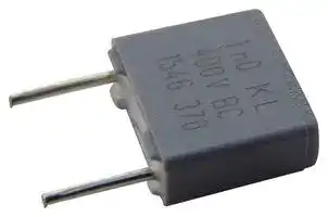
General Purpose Film Capacitor, Metallized PET, Radial Box - 2 Pin, 0.012 µF, ± 5%, 63 V, 100 V
- Manufacturer: VISHAY
- Product type: General Purpose Film Capacitors
- SVHC: No SVHC (04-Feb-2026)
- Capacitance: 0.012µF
- Voltage(AC): 63V
- Voltage(DC): 100V
- Lead Spacing: 5.08mm
- Product Range: MKT370 Series
- Product Width: 2.5mm
- Qualification: AEC-Q200
- Product Height: 6.5mm
- Product Length: 7.2mm
- Dielectric Type: Metallized PET
- Humidity Rating: GRADE II (Test Condition A)
- Capacitor Mounting: Through Hole
- Capacitor Terminals: PC Pin
- Capacitance Tolerance: ± 5%
- Capacitor Case / Package: Radial Box - 2 Pin
- Operating Temperature Max: 105°C
- Operating Temperature Min: -55°C
| Delivery and price | |
|---|---|
| Units per pack | 2000 |
| Price | 0.238 € |
| Current stock | 10+ |
| Lead time | 30 days |
**MKP339 X2** www.vishay.com Vishay BCcomponents ## **Interference Suppression Film Capacitors MKP Radial Potted Type** ## **FEATURES** **==> picture [38 x 68] intentionally omitted <==** - AEC-Q200 qualified (rev. C) up to 110 °C - THB: 40 °C / 93 % RH for 1000 h at rated voltage, in compliance with AEC-Q200 - Compliant with IEC 60384-14: AMD1 grade IA - High temperature capabilities, up to 125 °C - Material categorization: for definitions of compliance please see www.vishay.com/doc?99912 ## **APPLICATIONS** For standard across the line X2 applications. See also application note: www.vishay.com/doc?28153 |**QUICK REFERENCE DATA**|**QUICK REFERENCE DATA**|**QUICK REFERENCE DATA**|**QUICK REFERENCE DATA**| |---|---|---|---| |Rated capacitance range(E12 series)|0.001μF to 4.7μF(preferred values acc. to E6)||| |Capacitance tolerance|± 20 %; ± 10 %; ± 5 %||| |Rated voltage range, URAC|310 VAC; 50 Hz to 60 Hz||| |Permissible DC voltage|800 VDCat 85 °C<br>630 VDCat 110 °C||| |Climatic testing class|55/110/56/C for product volumes1750 mm3<br>55/110/56/B forproduct volumes > 1750 mm3||| |Rated temperature|110 °C||| |Maximum application temperature|125 °C for limited time||| |Reference standards|IEC 60384-14:2013<br>IEC 60384-14:2013 / AMD1:2016<br>EN 60384-14:2013 + AMD1:2016<br>IEC 60065 requires pass. flamm. class B for volumes > 1750 mm3<br>UL 60384-14<br>CSA-E384-14<br>CQC||| |Dielectric|||Polypropylene film| |Electrodes|||Metallized| |Construction|||Mono construction| |Encapsulation|Plastic case, epoxyresin sealed, flame retardant UL-class 94 V-0||| |Leads|Tinned wire||| |Marking|C-value; tolerance; rated voltage; sub-class; manufacturer’s type;<br>code for dielectric material, manufacturer location; manufacturer’s logo;<br>year and week; safetyapprovals||| ## **Note** - For more detailed data and test requirements, contact rfi@vishay.com ## **DIMENSIONS** in millimeters **==> picture [115 x 87] intentionally omitted <==** **----- Start of picture text -----**<br> l w<br>h<br>lt<br>P Ø dt<br>**----- End of picture text -----**<br> Revision: 19-Jul-2024 Document Number: 28138 **1** For technical questions, contact: rfi@vishay.com THIS DOCUMENT IS SUBJECT TO CHANGE WITHOUT NOTICE. THE PRODUCTS DESCRIBED HEREIN AND THIS DOCUMENT ARE SUBJECT TO SPECIFIC DISCLAIMERS, SET FORTH AT www.vishay.com/doc?91000 **MKP339 X2** Vishay BCcomponents **==> picture [77 x 10] intentionally omitted <==** **----- Start of picture text -----**<br> www.vishay.com<br>**----- End of picture text -----**<br> ## **COMPOSITION OF CATALOG NUMBER** |||**TYPE AND PITCHES**|**TYPE AND PITCHES**|**TYPE AND PITCHES**|**TYPE AND PITCHES**||||||||**MULTIPLIER**<br>**(nF)**<br>Example:<br>104 = 10 x 10 = 100 nF<br>0.1<br>2<br>3<br>4<br>5<br>100<br>10<br>1|**MULTIPLIER**<br>**(nF)**<br>Example:<br>104 = 10 x 10 = 100 nF<br>0.1<br>2<br>3<br>4<br>5<br>100<br>10<br>1|**MULTIPLIER**<br>**(nF)**<br>Example:<br>104 = 10 x 10 = 100 nF<br>0.1<br>2<br>3<br>4<br>5<br>100<br>10<br>1| |---|---|---|---|---|---|---|---|---|---|---|---|---|---|---|---| |||339<br>X2||7.5 mm|||||||||||| |||||10.0 mm||||**CAPACITANCE**<br>**(numerically)**|||||||| |||||15.0 mm|||||||||||| |||||22.5 mm|||||||||||| |||||27.5 mm|||||||||||| ||||||||||||||||| ||||||||||||||||| |||||BFC2||339|XX|||XX||X|||| ||||||||||||||||| ||||||||||||||||| ||||||||||||||||| |**E**<br>**P**<br>**Y**<br>**T**||**G**<br>**N**<br>**I**<br>**G**<br>**A**<br>**K**<br>**C**<br>**A**<br>**P**||||**S**<br>**N**<br>**O**<br>**I**<br>**S**<br>**N**<br>**E**<br>**M**<br>**I**<br>**D**<br>**D**<br>**R**<br>**A**<br>**D**<br>**N**<br>**A**<br>**T**<br>**S**||||||||**.**<br>**L**<br>**O**<br>**T**<br>**-**<br>**C**|**R**<br>**E**<br>**B**<br>**M**<br>**U**<br>**N**<br>**E**<br>**D**<br>**O**<br>**C**| |339<br>X2||Loose in box|||Lead length 3.5 mm + 1 mm/- 0.5 mm or 3.5 mm ± 0.3 mm|||||||||± 20 %|BFC2 339 20...| ||||||m<br>m<br>0<br>.<br>1<br>±<br>m<br>m<br>0<br>.<br>5<br>h<br>t<br>g<br>n<br>el<br>d<br>a<br>e<br>L||||||||||...<br>2<br>2<br>9<br>3<br>3<br>2<br>C<br>F<br>B| ||||||m<br>m<br>0<br>.<br>2<br>±<br>m<br>m<br>0<br>.<br>5<br>2<br>h<br>t<br>g<br>n<br>el<br>d<br>a<br>e<br>L||||||||||...<br>4<br>2<br>9<br>3<br>3<br>2<br>C<br>F<br>B| |||Taped(1)|||Reel: H = 18.5 mm;P0<br>m<br>m<br>0<br>.<br>5<br>1<br>r<br>o<br>m<br>m<br>7<br>.<br>2<br>1<br>=||||||||||...<br>6<br>2<br>9<br>3<br>3<br>2<br>C<br>F<br>B| ||||||Ammopack: H = 18.5 mm;P0<br>m<br>m<br>7<br>.<br>2<br>1<br>=||||||||||...<br>8<br>2<br>9<br>3<br>3<br>2<br>C<br>F<br>B| |||Loose in box|||Lead length 3.5 mm + 1 mm/- 0.5 mm or 3.5 mm ± 0.3 mm|||||||||± 10 %|BFC2 339 10...| ||||||m<br>m<br>0<br>.<br>1<br>±<br>m<br>m<br>0<br>.<br>5<br>h<br>t<br>g<br>n<br>el<br>d<br>a<br>e<br>L||||||||||...<br>2<br>1<br>9<br>3<br>3<br>2<br>C<br>F<br>B| ||||||m<br>m<br>0<br>.<br>2<br>±<br>m<br>m<br>0<br>.<br>5<br>2<br>h<br>t<br>g<br>n<br>el<br>d<br>a<br>e<br>L||||||||||...<br>4<br>1<br>9<br>3<br>3<br>2<br>C<br>F<br>B| |||Taped(1)|||Reel: H = 18.5 mm;P0<br>m<br>m<br>0<br>.<br>5<br>1<br>r<br>o<br>m<br>m<br>7<br>.<br>2<br>1<br>=||||||||||...<br>6<br>1<br>9<br>3<br>3<br>2<br>C<br>F<br>B| ||||||Ammopack: H = 18.5 mm;P0<br>m<br>m<br>7<br>.<br>2<br>1<br>=||||||||||...<br>8<br>1<br>9<br>3<br>3<br>2<br>C<br>F<br>B| |||Loose in box|||Lead length 3.5 mm + 1 mm/- 0.5 mm or 3.5 mm ± 0.3 mm|||||||||± 5 %|BFC2 339 50...| ||||||m<br>m<br>0<br>.<br>1<br>±<br>m<br>m<br>0<br>.<br>5<br>h<br>t<br>g<br>n<br>el<br>d<br>a<br>e<br>L||||||||||...<br>2<br>5<br>9<br>3<br>3<br>2<br>C<br>F<br>B| ||||||m<br>m<br>0<br>.<br>2<br>±<br>m<br>m<br>0<br>.<br>5<br>2<br>h<br>t<br>g<br>n<br>el<br>d<br>a<br>elL||||||||||...<br>4<br>5<br>9<br>3<br>3<br>2<br>C<br>F<br>B| |||Taped(1)|||Reel: H = 18.5 mm;P0<br>m<br>m<br>0<br>.<br>5<br>1<br>r<br>o<br>m<br>m<br>7<br>.<br>2<br>1<br>=||||||||||...<br>6<br>3<br>9<br>3<br>3<br>2<br>C<br>F<br>B| ||||||Ammopack: H = 18.5 mm;P0<br>m<br>m<br>7<br>.<br>2<br>1<br>=||||||||||...<br>8<br>3<br>9<br>3<br>3<br>2<br>C<br>F<br>B| |||**PACKAGING**|||**ALTERNATIVE LARGER PITCH SIZES**|||||||||**C-TOL.**|**CODE NUMBER**| |||Loose in box|||Lead length 3.5 mm + 1 mm/- 0.5 mm or 3.5 mm ± 0.3 mm|||||||||± 20 %|BFC2 339 21...| ||||||m<br>m<br>0<br>.<br>1<br>±<br>m<br>m<br>0<br>.<br>5<br>h<br>t<br>g<br>n<br>el<br>d<br>a<br>e<br>L||||||||||...<br>3<br>2<br>9<br>3<br>3<br>2<br>C<br>F<br>B| ||||||m<br>m<br>0<br>.<br>2<br>±<br>m<br>m<br>0<br>.<br>5<br>2<br>h<br>t<br>g<br>n<br>el<br>d<br>a<br>e<br>L||||||||||...<br>5<br>2<br>9<br>3<br>3<br>2<br>C<br>F<br>B| |||Taped(1)(2)|||Reel or ammopack: H = 18.5 mm;P0<br>m<br>m<br>7<br>.<br>2<br>1<br>=||||||||||...<br>7<br>2<br>9<br>3<br>3<br>2<br>C<br>F<br>B| |||Loose in box|||Lead length 3.5 mm + 1 mm/- 0.5 mm or 3.5 mm ± 0.3 mm|||||||||± 10 %|BFC2 339 11...| ||||||m<br>m<br>0<br>.<br>1<br>±<br>m<br>m<br>0<br>.<br>5<br>h<br>t<br>g<br>n<br>el<br>d<br>a<br>e<br>L||||||||||...<br>3<br>1<br>9<br>3<br>3<br>2<br>C<br>F<br>B| ||||||m<br>m<br>0<br>.<br>2<br>±<br>m<br>m<br>0<br>.<br>5<br>2<br>h<br>t<br>g<br>n<br>el<br>d<br>a<br>e<br>L||||||||||...<br>5<br>1<br>9<br>3<br>3<br>2<br>C<br>F<br>B| |||Taped(1)(2)|||Reel or ammopack: H = 18.5 mm;P0<br>m<br>m<br>7<br>.<br>2<br>1<br>=||||||||||...<br>7<br>1<br>9<br>3<br>3<br>2<br>C<br>F<br>B| |||Loose in box|||Lead length 3.5 mm + 1 mm/- 0.5 mm or 3.5 mm ± 0.3 mm|||||||||± 5 %|BFC2 339 51...| ||||||m<br>m<br>0<br>.<br>1<br>±<br>m<br>m<br>0<br>.<br>5<br>h<br>t<br>g<br>n<br>el<br>d<br>a<br>e<br>L||||||||||...<br>3<br>5<br>9<br>3<br>3<br>2<br>C<br>F<br>B| ||||||m<br>m<br>0<br>.<br>2<br>±<br>m<br>m<br>0<br>.<br>5<br>2<br>h<br>t<br>g<br>n<br>el<br>d<br>a<br>e<br>L||||||||||...<br>5<br>5<br>9<br>3<br>3<br>2<br>C<br>F<br>B| |||Taped(1)(2)|||Reel: H = 18.5 mm;P0<br>m<br>m<br>0<br>.<br>5<br>1<br>r<br>o<br>m<br>m<br>7<br>.<br>2<br>1<br>=||||||||||...<br>6<br>4<br>9<br>3<br>3<br>2<br>C<br>F<br>B| ||||||Ammopack: H = 18.5 mm;P0<br>m<br>m<br>7<br>.<br>2<br>1<br>=||||||||||...<br>8<br>4<br>9<br>3<br>3<br>2<br>C<br>F<br>B| ## **Notes** > (1) For detailed tape specification refer to “Packaging Information”: www.vishay.com/doc?28139 > (2) Taped on reel pitch = 27.5 mm is not available Revision: 19-Jul-2024 Document Number: 28138 **2** For technical questions, contact: rfi@vishay.com THIS DOCUMENT IS SUBJECT TO CHANGE WITHOUT NOTICE. THE PRODUCTS DESCRIBED HEREIN AND THIS DOCUMENT ARE SUBJECT TO SPECIFIC DISCLAIMERS, SET FORTH AT www.vishay.com/doc?91000 **MKP339 X2** www.vishay.com ## Vishay BCcomponents |**SPECIFIC REFERENCE DATA**||| |---|---|---| |**DESCRIPTION**|**VALUE**|| |Rated AC voltage (URAC)|310 V|| |Permissible DC voltage (URDC)|630 V|| |Tangent of loss angle:<br>C < 470 nF<br>470 nFC1 μF<br>C > 1 μF|at 1 kHz|at 10 kHz| ||10 x 10-4<br>20 x 10-4<br>30 x 10-4|20 x 10-4<br>70 x 10-4<br>-| |Rated voltage pulse slope (dU/dt)Rat 435 VDC:<br>Pitch = 7.5 mm<br>Pitch = 10 mm<br>Pitch = 15 mm<br>Pitch = 22.5 mm<br>Pitch = 27.5 mm|600 V/μs<br>600 V/μs<br>400 V/μs<br>150 V/μs<br>100 V/μs|| |R between leads, for C0.33 μF at 100 V; 1 min|> 15 000 M|| |RC between leads, for C > 0.33 μF at 100 V; 1 min|> 5000 s|| |R between leads and case; 100 V; 1 min|> 30 000 M|| |Withstanding (DC) voltage (cut off current 10 mA)(1); rise time1000 V/s:<br>C1 μF<br>C > 1 μF|2200 V; 1 min<br>1800 V; 1 min|| |Withstanding (AC) voltage between leads and case|2120 V; 1 min|| |Max. application temperature for 0.001 μFC0.47 μF|125 °C up to 1000 h|| |Max. application temperature for C > 0.47 μF|125 °C up to 500 h|| ## **Note** > (1) See “Voltage Proof Test for Metalized Film Capacitors”: www.vishay.com/doc?28169 ## **ELECTRICAL DATA AND ORDERING INFORMATION - PITCH: 7.5 mm** |**ELECTRICAL DATA AND ORDERING INFORMATION - PITCH: 7.5 mm**|**ELECTRICAL DATA AND ORDERING INFORMATION - PITCH: 7.5 mm**|**ELECTRICAL DATA AND ORDERING INFORMATION - PITCH: 7.5 mm**|**ELECTRICAL DATA AND ORDERING INFORMATION - PITCH: 7.5 mm**|**ELECTRICAL DATA AND ORDERING INFORMATION - PITCH: 7.5 mm**|**ELECTRICAL DATA AND ORDERING INFORMATION - PITCH: 7.5 mm**|**ELECTRICAL DATA AND ORDERING INFORMATION - PITCH: 7.5 mm**|**ELECTRICAL DATA AND ORDERING INFORMATION - PITCH: 7.5 mm**|**ELECTRICAL DATA AND ORDERING INFORMATION - PITCH: 7.5 mm**|**ELECTRICAL DATA AND ORDERING INFORMATION - PITCH: 7.5 mm**|**ELECTRICAL DATA AND ORDERING INFORMATION - PITCH: 7.5 mm**| |---|---|---|---|---|---|---|---|---|---|---| |**URAC**<br>**(V)**|**CAP.**<br>**(μF)**|**DIMENSIONS(1)**<br>**w x h x l**<br>**(mm)**|**MASS**<br>**(g)(2)**|**CATALOG NUMBER BFC2 339 XXXXX AND PACKAGING**||||||| |||||**LOOSE IN BOX**|||||**AMMOPACK(3)**|| |||||**SHORT LEADS**|||**LONG LEADS**||**H = 18.5 mm**<br>**P0 = 12.7 mm**|| |||||**It = 3.5 mm**<br>**+ 1 mm/- 0.5 mm**|**It = 5.0 mm**<br>**± 1.0 mm**|**SPQ**|**It = 25.0 mm**<br>**± 2.0 mm**|**SPQ**||**SPQ**| |310|**PITCH = 7.5 mm ± 0.4 mm; dt = 0.50 m**|||**m ± 0.05 mm; C-TOL. = ± 20 %**||||||| ||0.0010<br>0.0015<br>0.0022<br>0.0033<br>0.0047<br>0.0068<br>0.010<br>0.015<br>0.022<br>0.033|4.0 x 9.0 x 10.0|0.4|20102<br>20152<br>20222<br>20332<br>20472<br>20682<br>20103<br>20153<br>20223<br>20333|22102<br>22152<br>22222<br>22332<br>22472<br>22682<br>22103<br>22153<br>22223<br>22333|1500|24102<br>24152<br>24222<br>24332<br>24472<br>24682<br>24103<br>24153<br>24223<br>24333|1000|28102<br>28152<br>28222<br>28332<br>28472<br>28682<br>28103<br>28153<br>28223<br>28333|1250| ||0.047|5.0 x 10.5 x 10.0|0.4|20473|22473|1000|24473|1250|28473|1000| ||0.068|6.0 x 11.5 x 10.0|0.8|20683|22683|750|24683|1000|28683|750| Document Number: 28138 Revision: 19-Jul-2024 **3** For technical questions, contact: rfi@vishay.com THIS DOCUMENT IS SUBJECT TO CHANGE WITHOUT NOTICE. THE PRODUCTS DESCRIBED HEREIN AND THIS DOCUMENT ARE SUBJECT TO SPECIFIC DISCLAIMERS, SET FORTH AT www.vishay.com/doc?91000 **MKP339 X2** www.vishay.com Vishay BCcomponents |**ELECTRICAL DATA AND ORDERING INFORMATION - PITCH: 7.5 mm**|**ELECTRICAL DATA AND ORDERING INFORMATION - PITCH: 7.5 mm**|**ELECTRICAL DATA AND ORDERING INFORMATION - PITCH: 7.5 mm**|**ELECTRICAL DATA AND ORDERING INFORMATION - PITCH: 7.5 mm**|**ELECTRICAL DATA AND ORDERING INFORMATION - PITCH: 7.5 mm**|**ELECTRICAL DATA AND ORDERING INFORMATION - PITCH: 7.5 mm**|**ELECTRICAL DATA AND ORDERING INFORMATION - PITCH: 7.5 mm**|**ELECTRICAL DATA AND ORDERING INFORMATION - PITCH: 7.5 mm**|**ELECTRICAL DATA AND ORDERING INFORMATION - PITCH: 7.5 mm**|**ELECTRICAL DATA AND ORDERING INFORMATION - PITCH: 7.5 mm**|**ELECTRICAL DATA AND ORDERING INFORMATION - PITCH: 7.5 mm**| |---|---|---|---|---|---|---|---|---|---|---| |**URAC**<br>**(V)**|**CAP.**<br>**(μF)**|**DIMENSIONS(1)**<br>**w x h x l**<br>**(mm)**|**MASS**<br>**(g)(2)**|**CATALOG NUMBER BFC2 339 XXXXX AND PACKAGING**||||||| |||||**LOOSE IN BOX**|||||**AMMOPACK(3)**|| |||||**SHORT LEADS**|||**LONG LEADS**||**H = 18.5 mm**<br>**P0 = 12.7 mm**|| |||||**It = 3.5 mm**<br>**+ 1 mm/- 0.5 mm**|**It = 5.0 mm**<br>**± 1.0 mm**|**SPQ**|**It = 25.0 mm**<br>**± 2.0 mm**|**SPQ**||**SPQ**| |310|**PITCH = 7.5 mm ± 0.4 mm; dt = 0.50 m**|||**m ± 0.05 mm; C-TOL. = ± 10 %**||||||| ||0.0010<br>0.0012<br>0.0015<br>0.0018<br>0.0022<br>0.0027<br>0.0033<br>0.0039<br>0.0047<br>0.0056<br>0.0068<br>0.0082<br>0.010<br>0.012<br>0.015<br>0.018<br>0.022<br>0.027|4.0 x 9.0 x 10.0|0.45|10102<br>10122<br>10152<br>10182<br>10222<br>10272<br>10332<br>10392<br>10472<br>10562<br>10682<br>10822<br>10103<br>10123<br>10153<br>10183<br>10223<br>10273|12102<br>12122<br>12152<br>12182<br>12222<br>12272<br>12332<br>12392<br>12472<br>12562<br>12682<br>12822<br>12103<br>12123<br>12153<br>12183<br>12223<br>12273|1500|14102<br>14122<br>14152<br>14182<br>14222<br>14272<br>14332<br>14392<br>14472<br>14562<br>14682<br>14822<br>14103<br>14123<br>14153<br>14183<br>14223<br>14273|1000|18102<br>18122<br>18152<br>18182<br>18222<br>18272<br>18332<br>18392<br>18472<br>18562<br>18682<br>18822<br>18103<br>18123<br>18153<br>18183<br>18223<br>18273|1250| ||0.033<br>0.039<br>0.047|5.0 x 10.5 x 10.0|0.6|10333<br>10393<br>10473|12333<br>12393<br>12473|1000|14333<br>14393<br>14473|1250|18333<br>18393<br>18473|1000| ||0.056|6.0 x 11.5 x 10.0|0.8|10563|12563|750|14563|1000|18563|750| ||**PITCH = 7.5 mm ± 0.4 mm; dt = 0.50 m**|||**m ± 0.05 mm; C-TOL. = ± 5 %**||||||| ||0.0010<br>0.0012<br>0.0015<br>0.0018<br>0.0022<br>0.0027<br>0.0033<br>0.0039<br>0.0047<br>0.0056<br>0.0068<br>0.0082<br>0.010<br>0.012<br>0.015<br>0.018<br>0.022<br>0.027|4.0 x 9.0 x 10.0|0.45|50102<br>50122<br>50152<br>50182<br>50222<br>50272<br>50332<br>50392<br>50472<br>50562<br>50682<br>50822<br>50103<br>50123<br>50153<br>50183<br>50223<br>50273|52102<br>52122<br>52152<br>52182<br>52222<br>52272<br>52332<br>52392<br>52472<br>52562<br>52682<br>52822<br>52103<br>52123<br>52153<br>52183<br>52223<br>52273|1500|54102<br>54122<br>54152<br>54182<br>54222<br>54272<br>54332<br>54392<br>54472<br>54562<br>54682<br>54822<br>54103<br>54123<br>54153<br>54183<br>54223<br>54273|1000|38102<br>38122<br>38152<br>38182<br>38222<br>38272<br>38332<br>38392<br>38472<br>38562<br>38682<br>38822<br>38103<br>38123<br>38153<br>38183<br>38223<br>38273|1250| ||0.033<br>0.039|5.0 x 10.5 x 10.0|0.6|50333<br>50393|52333<br>52393|1000|54333<br>54393|1250|38333<br>38393|1000| ||0.047<br>0.056|6.0 x 11.5 x 10.0|0.8|50473<br>50563|52473<br>52563|750|54473<br>54563|1000|38473<br>38563|750| ## **Notes** - SPQ = Standard Packing Quantity > (1) For tolerances see section “Space Requirements for Printed-Circuit Board Applications and Dimension Tolerances” - (2) Weight for short lead product only - (3) H = in-tape height; P0 = sprocket hole distance; for detailed specifications refer to packaging information Revision: 19-Jul-2024 Document Number: 28138 **4** For technical questions, contact: rfi@vishay.com THIS DOCUMENT IS SUBJECT TO CHANGE WITHOUT NOTICE. THE PRODUCTS DESCRIBED HEREIN AND THIS DOCUMENT ARE SUBJECT TO SPECIFIC DISCLAIMERS, SET FORTH AT www.vishay.com/doc?91000 **MKP339 X2** www.vishay.com Vishay BCcomponents |**ELECTRICAL DATA AND ORDERING INFORMATION - PITCH: 10 mm**|**ELECTRICAL DATA AND ORDERING INFORMATION - PITCH: 10 mm**|**ELECTRICAL DATA AND ORDERING INFORMATION - PITCH: 10 mm**|**ELECTRICAL DATA AND ORDERING INFORMATION - PITCH: 10 mm**|**ELECTRICAL DATA AND ORDERING INFORMATION - PITCH: 10 mm**|**ELECTRICAL DATA AND ORDERING INFORMATION - PITCH: 10 mm**|**ELECTRICAL DATA AND ORDERING INFORMATION - PITCH: 10 mm**|**ELECTRICAL DATA AND ORDERING INFORMATION - PITCH: 10 mm**|**ELECTRICAL DATA AND ORDERING INFORMATION - PITCH: 10 mm**|**ELECTRICAL DATA AND ORDERING INFORMATION - PITCH: 10 mm**|**ELECTRICAL DATA AND ORDERING INFORMATION - PITCH: 10 mm**|**ELECTRICAL DATA AND ORDERING INFORMATION - PITCH: 10 mm**|**ELECTRICAL DATA AND ORDERING INFORMATION - PITCH: 10 mm**| |---|---|---|---|---|---|---|---|---|---|---|---|---| |**URAC**<br>**(V)**|**CAP.**<br>**(μF)**|**DIMENSIONS(1)**<br>**w x h x l**<br>**(mm)**|**MASS**<br>**(g)(2)**|**CATALOG NUMBER BFC2 339 XXXXX AND PACKAGING**||||||||| |||||**LOOSE IN BOX**|||||**AMMOPACK(3)**||**LARGE REEL**<br>**(500 mm)(3)(4)**|| |||||**SHORT LEADS**|||**LONG LEADS**||**H = 18.5 mm**<br>**P0 = 12.7 mm**||**H = 18.5.mm**<br>**P0 = 12.7 mm**|| |||||**It = 3.5 mm**<br>**+ 1 mm/- 0.5 mm**|**It = 5.0 mm**<br>**± 1.0 mm**|**SPQ**|**It = 25.0 mm**<br>**± 2.0 mm**|**SPQ**||**SPQ**||**SPQ**| |310|**PITCH = 10.0 mm ± 0.4 mm; dt =**|||**0.60 mm ± 0.06 mm; C-TOL. = ± 20 %**||||||||| ||0.0010<br>0.0015<br>0.0022<br>0.0033<br>0.0047<br>0.0068<br>0.010<br>0.015<br>0.022<br>0.033<br>0.047|4.0 x 10.0 x 12.5|0.6|21102<br>21152<br>21222<br>21332<br>21472<br>21682<br>21103<br>21153<br>21223<br>21333<br>21473|23102<br>23152<br>23222<br>23332<br>23472<br>23682<br>23103<br>23153<br>23223<br>23333<br>23473|1000|25102<br>25152<br>25222<br>25332<br>25472<br>25682<br>25103<br>25153<br>25223<br>25333<br>25473|1250|27102<br>27152<br>27222<br>27332<br>27472<br>27682<br>27103<br>27153<br>27223<br>27333<br>27473|950|-|-| ||0.068|5.0 x 11.0 x 12.5|0.82|21683|23683|1000|25683|1000|27683|750|-|-| ||0.100|6.0 x 12.0 x 12.5|1.1|20104|22104|750|24104|750|28104|600|26104|900| ||**PITCH = 10.0 mm ± 0.4 mm; dt =**|||**0.60 mm ± 0.06 mm; C-TOL. = ± 10 %**||||||||| ||0.0010<br>0.0012<br>0.0015<br>0.0018<br>0.0022<br>0.0027<br>0.0033<br>0.0039<br>0.0047<br>0.0056<br>0.0068<br>0.0082<br>0.010<br>0.012<br>0.015<br>0.018<br>0.022<br>0.027<br>0.033<br>0.039<br>0.047|4.0 x 10.0 x 12.5|0.6|11102<br>11122<br>11152<br>11182<br>11222<br>11272<br>11332<br>11392<br>11472<br>11562<br>11682<br>11822<br>11103<br>11123<br>11153<br>11183<br>11223<br>11273<br>11333<br>11393<br>11473|13102<br>13122<br>13152<br>13182<br>13222<br>13272<br>13332<br>13392<br>13472<br>13562<br>13682<br>13822<br>13103<br>13123<br>13153<br>13183<br>13223<br>13273<br>13333<br>13393<br>13473|1000|15102<br>15122<br>15152<br>15182<br>15222<br>15272<br>15332<br>15392<br>15472<br>15562<br>15682<br>15822<br>15103<br>15123<br>15153<br>15183<br>15223<br>15273<br>15333<br>15393<br>15473|1250|17102<br>17122<br>17152<br>17182<br>17222<br>17272<br>17332<br>17392<br>17472<br>17562<br>17682<br>17822<br>17103<br>17123<br>17153<br>17183<br>17223<br>17273<br>17333<br>17393<br>17473|950|-|-| ||0.056<br>0.068|5.0 x 11.0 x 12.5|0.82|11563<br>10683|13563<br>12683|1000|15563<br>14683|1000|17563<br>18683|750|-<br>16683|-<br>1100| ||0.082<br>0.100|6.0 x 12.0 x 12.5|1.1|10823<br>10104|12823<br>12104|750|14823<br>14104|750|18823<br>18104|600|16823<br>16104|900| Revision: 19-Jul-2024 Document Number: 28138 **5** For technical questions, contact: rfi@vishay.com THIS DOCUMENT IS SUBJECT TO CHANGE WITHOUT NOTICE. THE PRODUCTS DESCRIBED HEREIN AND THIS DOCUMENT ARE SUBJECT TO SPECIFIC DISCLAIMERS, SET FORTH AT www.vishay.com/doc?91000 **MKP339 X2** www.vishay.com Vishay BCcomponents |**ELECTRICAL DATA AND ORDERING INFORMATION - PITCH: 10 mm**|**ELECTRICAL DATA AND ORDERING INFORMATION - PITCH: 10 mm**|**ELECTRICAL DATA AND ORDERING INFORMATION - PITCH: 10 mm**|**ELECTRICAL DATA AND ORDERING INFORMATION - PITCH: 10 mm**|**ELECTRICAL DATA AND ORDERING INFORMATION - PITCH: 10 mm**|**ELECTRICAL DATA AND ORDERING INFORMATION - PITCH: 10 mm**|**ELECTRICAL DATA AND ORDERING INFORMATION - PITCH: 10 mm**|**ELECTRICAL DATA AND ORDERING INFORMATION - PITCH: 10 mm**|**ELECTRICAL DATA AND ORDERING INFORMATION - PITCH: 10 mm**|**ELECTRICAL DATA AND ORDERING INFORMATION - PITCH: 10 mm**|**ELECTRICAL DATA AND ORDERING INFORMATION - PITCH: 10 mm**|**ELECTRICAL DATA AND ORDERING INFORMATION - PITCH: 10 mm**|**ELECTRICAL DATA AND ORDERING INFORMATION - PITCH: 10 mm**| |---|---|---|---|---|---|---|---|---|---|---|---|---| |**URAC**<br>**(V)**|**CAP.**<br>**(μF)**|**DIMENSIONS(1)**<br>**w x h x l**<br>**(mm)**|**MASS**<br>**(g)(2)**|**CATALOG NUMBER BFC2 339 XXXXX AND PACKAGING**||||||||| |||||**LOOSE IN BOX**|||||**AMMOPACK(3)**||**LARGE REEL**<br>**(500 mm)(3)(4)**|| |||||**SHORT LEADS**|||**LONG LEADS**||**H = 18.5 mm**<br>**P0 = 12.7 mm**||**H = 18.5.mm**<br>**P0 = 12.7 mm**|| |||||**It = 3.5 mm**<br>**+ 1 mm/- 0.5 mm**|**It = 5.0 mm**<br>**± 1.0 mm**|**SPQ**|**It = 25.0 mm**<br>**± 2.0 mm**|**SPQ**||**SPQ**||**SPQ**| |310|**PITCH = 10.0 mm ± 0.4 mm; dt =**|||**0.60 mm ± 0.06 mm; C-TOL. = ± 5 %**||||||||| ||0.0010<br>0.0012<br>0.0015<br>0.0018<br>0.0022<br>0.0027<br>0.0033<br>0.0039<br>0.0047<br>0.0056<br>0.0068<br>0.0082<br>0.010<br>0.012<br>0.015<br>0.018<br>0.022<br>0.027<br>0.033<br>0.039<br>0.047|4.0 x 10.0 x 12.5|0.6|51102<br>51122<br>51152<br>51182<br>51222<br>51272<br>51332<br>51392<br>51472<br>51562<br>51682<br>51822<br>51103<br>51123<br>51153<br>51183<br>51223<br>51273<br>51333<br>51393<br>51473|53102<br>53122<br>53152<br>53182<br>53222<br>53272<br>53332<br>53392<br>53472<br>53562<br>53682<br>53822<br>53103<br>53123<br>53153<br>53183<br>53223<br>53273<br>53333<br>53393<br>53473|1000|55102<br>55122<br>55152<br>55182<br>55222<br>55272<br>55332<br>55392<br>55472<br>55562<br>55682<br>55822<br>55103<br>55123<br>55153<br>55183<br>55223<br>55273<br>55333<br>55393<br>55473|1250|48102<br>48122<br>48152<br>48182<br>48222<br>48272<br>48332<br>48392<br>48472<br>48562<br>48682<br>48822<br>48103<br>48123<br>48153<br>48183<br>48223<br>48273<br>48333<br>48393<br>48473|950|-|-| ||0.056<br>0.068|5.0 x 11.0 x 12.5|0.82|51563<br>50683|53563<br>52683|1000|55563<br>54683|1000|48563<br>38683|750|46563<br>36683|1100| ||0.082|6.0 x 12.0 x 12.5|1.1|50823|52823|750|54823|750|38823|600|36823|900| ## **Notes** - SPQ = Standard Packing Quantity > (1) For tolerances see section “Space Requirements for Printed-Circuit Board Applications and Dimension Tolerances” - (2) Weight for short lead product only > (3) H = in-tape height; P0 = sprocket hole distance; for detailed specifications refer to packaging information - (4) Reel diameter = 356 mm is available on request Revision: 19-Jul-2024 Document Number: 28138 **6** For technical questions, contact: rfi@vishay.com THIS DOCUMENT IS SUBJECT TO CHANGE WITHOUT NOTICE. THE PRODUCTS DESCRIBED HEREIN AND THIS DOCUMENT ARE SUBJECT TO SPECIFIC DISCLAIMERS, SET FORTH AT www.vishay.com/doc?91000 **MKP339 X2** www.vishay.com Vishay BCcomponents |**ELECTRICAL DATA AND ORDERING INFORMATION - PITCH: 15 mm**|**ELECTRICAL DATA AND ORDERING INFORMATION - PITCH: 15 mm**|**ELECTRICAL DATA AND ORDERING INFORMATION - PITCH: 15 mm**|**ELECTRICAL DATA AND ORDERING INFORMATION - PITCH: 15 mm**|**ELECTRICAL DATA AND ORDERING INFORMATION - PITCH: 15 mm**|**ELECTRICAL DATA AND ORDERING INFORMATION - PITCH: 15 mm**|**ELECTRICAL DATA AND ORDERING INFORMATION - PITCH: 15 mm**|**ELECTRICAL DATA AND ORDERING INFORMATION - PITCH: 15 mm**|**ELECTRICAL DATA AND ORDERING INFORMATION - PITCH: 15 mm**|**ELECTRICAL DATA AND ORDERING INFORMATION - PITCH: 15 mm**|**ELECTRICAL DATA AND ORDERING INFORMATION - PITCH: 15 mm**| |---|---|---|---|---|---|---|---|---|---|---| |**URAC**<br>**(V)**|**CAP.**<br>**(μF)**|**DIMENSIONS(1)**<br>**w x h x l**<br>**(mm)**|**MASS**<br>**(g)(2)**|**CATALOG NUMBER BFC2 339 XXXXX AND PACKAGING**||||||| |||||**LOOSE IN BOX**|||||**LARGE REEL**<br>**(500 mm)(3)(4)**|| |||||**SHORT LEADS**|||**LONG LEADS**||**H = 18.5 mm**<br>**P0 = 12.7 mm**|| |||||**It = 3.5 mm**<br>**± 0.3 mm**|**It = 5.0 mm**<br>**± 1.0 mm**|**SPQ**|**It = 25.0 mm**<br>**± 2.0 mm**|**SPQ**||**SPQ**| |310|**PITCH = 15 mm ± 0.4 mm; dt = 0.60 mm**|||**± 0.06 mm; C-TOL. = ± 20 %**||||||| ||0.010<br>0.015<br>0.022<br>0.033<br>0.047<br>0.068<br>0.10|5.0 x 11.0 x 17.5|1|90001<br>90002<br>90003<br>90004<br>90005<br>90006<br>21104|90007<br>90008<br>90009<br>90011<br>90012<br>90013<br>23104|1250|90014<br>90015<br>90016<br>90017<br>90018<br>90019<br>25104|1000|90021<br>90022<br>90023<br>90024<br>90025<br>90026<br>27104|1100| ||0.15|6.0 x 12.0 x 17.5|1.4|20154|22154|1000|24154|1000|26154|900| ||**PITCH = 15 mm ± 0.4 mm; dt = 0.80 mm**|||**± 0.08 mm; C-TOL. = ± 20 %**||||||| ||0.22|7.0 x 13.5 x 17.5|1.8|20224|22224|750|24224|500|26224|800| ||0.33|8.5 x 15.0 x 17.5|2.4|20334|22334|750|24334|500|26334|650| ||0.47|10.0 x 16.5 x 17.5|3.0|20474|22474|500|24474|450|26474|600| |||8.5 x 17.5 x 18.0|3.1|90165|90166|300|90143|500|-|-| ||0.56|11.0 x 18.5 x 18.0|4.3|90174|90175|225|90176|350|-|-| ||0.68|11.0 x 18.5 x 18.0|5.5|90168|90169|225|90145|350|-|-| ||**PITCH = 15 mm ± 0.4 mm; dt = 0.60 mm**|||**± 0.06 mm; C-TOL. = ± 10 %**||||||| ||0.010<br>0.012<br>0.015<br>0.018<br>0.022<br>0.027<br>0.033<br>0.039<br>0.047<br>0.056<br>0.068<br>0.082<br>0.100|5.0 x 11.0 x 17.5|1.0|90027<br>90028<br>90029<br>90031<br>90032<br>90033<br>90034<br>90035<br>90036<br>90037<br>11683<br>11823<br>11104|90039<br>90041<br>90042<br>90043<br>90044<br>90045<br>90046<br>90047<br>90048<br>90049<br>13683<br>13823<br>13104|1250|90052<br>90053<br>90054<br>90055<br>90056<br>90057<br>90058<br>90059<br>90061<br>90062<br>15683<br>15823<br>15104|1000|90064<br>90065<br>90066<br>90067<br>90068<br>90069<br>90071<br>90072<br>90073<br>90074<br>17683<br>17823<br>17104|1100| ||0.12<br>0.15|6.0 x 12.0 x 17.5|1.4|10124<br>10154|12124<br>12154|1000|14124<br>14154|1000|16124<br>16154|900| ||**PITCH = 15 mm ± 0.4 mm; dt = 0.80 mm**|||**± 0.08 mm; C-TOL. = ± 10 %**||||||| ||0.18<br>0.22|7.0 x 13.5 x 17.5|1.8|10184<br>10224|12184<br>12224|750|14184<br>14224|500|16184<br>16224|800| ||0.27<br>0.33|8.5 x 15.0 x 17.5|2.4|10274<br>10334|12274<br>12334|750|14274<br>14334|500|16274<br>16334|650| ||0.39<br>0.47|10.0 x 16.5 x 17.5|3.0|10394<br>10474|12394<br>12474|500|14394<br>14474|450|16394<br>16474|600| ||0.56|11.0 x 18.5 x 18.0|4.3|90167|90157|225|90144|400|-|-| Revision: 19-Jul-2024 **7** Document Number: 28138 For technical questions, contact: rfi@vishay.com THIS DOCUMENT IS SUBJECT TO CHANGE WITHOUT NOTICE. THE PRODUCTS DESCRIBED HEREIN AND THIS DOCUMENT ARE SUBJECT TO SPECIFIC DISCLAIMERS, SET FORTH AT www.vishay.com/doc?91000 **MKP339 X2** www.vishay.com Vishay BCcomponents |**ELECTRICAL DATA AND ORDERING INFORMATION - PITCH: 15 mm**|**ELECTRICAL DATA AND ORDERING INFORMATION - PITCH: 15 mm**|**ELECTRICAL DATA AND ORDERING INFORMATION - PITCH: 15 mm**|**ELECTRICAL DATA AND ORDERING INFORMATION - PITCH: 15 mm**|**ELECTRICAL DATA AND ORDERING INFORMATION - PITCH: 15 mm**|**ELECTRICAL DATA AND ORDERING INFORMATION - PITCH: 15 mm**|**ELECTRICAL DATA AND ORDERING INFORMATION - PITCH: 15 mm**|**ELECTRICAL DATA AND ORDERING INFORMATION - PITCH: 15 mm**|**ELECTRICAL DATA AND ORDERING INFORMATION - PITCH: 15 mm**|**ELECTRICAL DATA AND ORDERING INFORMATION - PITCH: 15 mm**|**ELECTRICAL DATA AND ORDERING INFORMATION - PITCH: 15 mm**| |---|---|---|---|---|---|---|---|---|---|---| |**URAC**<br>**(V)**|**CAP.**<br>**(μF)**|**DIMENSIONS(1)**<br>**w x h x l**<br>**(mm)**|**MASS**<br>**(g)(2)**|**CATALOG NUMBER BFC2 339 XXXXX AND PACKAGING**||||||| |||||**LOOSE IN BOX**|||||**LARGE REEL**<br>**(500 mm)(3)(4)**|| |||||**SHORT LEADS**|||**LONG LEADS**||**H = 18.5 mm**<br>**P0 = 12.7 mm**|| |||||**It = 3.5 mm**<br>**± 0.3 mm**|**It = 5.0 mm**<br>**± 1.0 mm**|**SPQ**|**It = 25.0 mm**<br>**± 2.0 mm**|**SPQ**||**SPQ**| |310|**PITCH = 15 mm ± 0.4 mm; dt = 0.60 mm**|||**± 0.06 mm; C-TOL. = ± 5 %**||||||| ||0.010<br>0.012<br>0.015<br>0.018<br>0.022<br>0.027<br>0.033<br>0.039<br>0.047<br>0.056<br>0.068<br>0.082<br>0.10|5.0 x 11.0 x 17.5|1.0|90221<br>90222<br>90223<br>90224<br>90225<br>90226<br>90227<br>90228<br>90229<br>90231<br>51683<br>51823<br>50104|90232<br>90233<br>90234<br>90235<br>90236<br>90237<br>90238<br>90239<br>90241<br>90242<br>53683<br>53823<br>52104|1250|90243<br>90244<br>90245<br>90246<br>90247<br>90248<br>90249<br>90251<br>90252<br>90253<br>55683<br>55823<br>54104|1000|90254<br>90255<br>90256<br>90257<br>90258<br>90259<br>90261<br>90262<br>90263<br>90264<br>46683<br>46823<br>36104|1100| ||0.12<br>0.15|6.0 x 12.0 x 17.5|1.4|50124<br>50154|52124<br>52154|1000|54124<br>54154|1000|36124<br>36154|900| ||**PITCH = 15 mm ± 0.4 mm; dt = 0.80 mm**|||**± 0.08 mm; C-TOL. = ± 5 %**||||||| ||0.18|7.0 x 13.5 x 17.5|1.8|50184|52184|750|54184|500|36184|800| ||0.22<br>0.27<br>0.33|8.5 x 15.0 x 17.5|2.4|50224<br>50274<br>50334|52224<br>52274<br>52334|750|54224<br>54274<br>54334|500|36224<br>36274<br>36334|650| ||0.39|10.0 x 16.5 x 17.5|3.0|50394|52394|500|54394|450|36394|600| ## **Notes** - SPQ = Standard Packing Quantity > (1) For tolerances see section “Space Requirements for Printed-Circuit Board Applications and Dimension Tolerances” - (2) Weight for short lead product only > (3) H = in-tape height; P0 = sprocket hole distance; for detailed specifications refer to packaging information - (4) Reel diameter = 356 mm is available on request ## **ELECTRICAL DATA AND ORDERING INFORMATION - PITCH: 22.5 mm** |**ELECTRICAL DATA AND ORDERING INFORMATION - PITCH: 22.5 mm**|**ELECTRICAL DATA AND ORDERING INFORMATION - PITCH: 22.5 mm**|**ELECTRICAL DATA AND ORDERING INFORMATION - PITCH: 22.5 mm**|**ELECTRICAL DATA AND ORDERING INFORMATION - PITCH: 22.5 mm**|**ELECTRICAL DATA AND ORDERING INFORMATION - PITCH: 22.5 mm**|**ELECTRICAL DATA AND ORDERING INFORMATION - PITCH: 22.5 mm**|**ELECTRICAL DATA AND ORDERING INFORMATION - PITCH: 22.5 mm**|**ELECTRICAL DATA AND ORDERING INFORMATION - PITCH: 22.5 mm**|**ELECTRICAL DATA AND ORDERING INFORMATION - PITCH: 22.5 mm**|**ELECTRICAL DATA AND ORDERING INFORMATION - PITCH: 22.5 mm**|**ELECTRICAL DATA AND ORDERING INFORMATION - PITCH: 22.5 mm**| |---|---|---|---|---|---|---|---|---|---|---| |**URAC**<br>**(V)**|**CAP.**<br>**(μF)**|**DIMENSIONS(1)**<br>**w x h x l**<br>**(mm)**|**MASS**<br>**(g)(2)**|**CATALOG NUMBER BFC2 339 XXXXX AND PACKAGING**||||||| |||||**LOOSE IN BOX**|||||**LARGE REEL**<br>**(500 mm)(3)(4)**|| |||||**SHORT LEADS**|||**LONG LEADS**||**H = 18.5 mm**<br>**P0 = 12.7 mm**|| |||||**It = 3.5 mm**<br>**± 0.3 mm**|**It = 5.0 mm**<br>**± 1.0 mm**|**SPQ**|**It = 25.0 mm**<br>**± 2.0 mm**|**SPQ**||**SPQ**| |310|**PITCH = 22.5 mm ± 0.4 mm; dt = 0.80 m**|||**m ± 0.08 mm; C-TOL. = ± 20 %**||||||| ||0.15<br>0.22<br>0.33|6.0 x 15.5 x 26.0|2.4|21154<br>21224<br>21334|23154<br>23224<br>23334|300|25154<br>25224<br>25334|250|27154<br>27224<br>27334|600| ||0.47|7.0 x 16.5 x 26.0|2.9|21474|23474|200|25474|250|27474|500| ||0.68|8.5 x 18.0 x 26.0|3.8|20684|22684|200|24684|250|26684|450| ||1.0|10.0 x 19.5 x 26.0|6.8|20105|22105|200|24105|200|26105|350| ||1.5|12.5 x 22.5 x 26.5|10|90103|90138|140|90139|400|90141|300| Revision: 19-Jul-2024 Document Number: 28138 **8** For technical questions, contact: rfi@vishay.com THIS DOCUMENT IS SUBJECT TO CHANGE WITHOUT NOTICE. THE PRODUCTS DESCRIBED HEREIN AND THIS DOCUMENT ARE SUBJECT TO SPECIFIC DISCLAIMERS, SET FORTH AT www.vishay.com/doc?91000 **MKP339 X2** www.vishay.com Vishay BCcomponents |**ELECTRICAL DATA AND ORDERING INFORMATION - PITCH: 22.5 mm**|**ELECTRICAL DATA AND ORDERING INFORMATION - PITCH: 22.5 mm**|**ELECTRICAL DATA AND ORDERING INFORMATION - PITCH: 22.5 mm**|**ELECTRICAL DATA AND ORDERING INFORMATION - PITCH: 22.5 mm**|**ELECTRICAL DATA AND ORDERING INFORMATION - PITCH: 22.5 mm**|**ELECTRICAL DATA AND ORDERING INFORMATION - PITCH: 22.5 mm**|**ELECTRICAL DATA AND ORDERING INFORMATION - PITCH: 22.5 mm**|**ELECTRICAL DATA AND ORDERING INFORMATION - PITCH: 22.5 mm**|**ELECTRICAL DATA AND ORDERING INFORMATION - PITCH: 22.5 mm**|**ELECTRICAL DATA AND ORDERING INFORMATION - PITCH: 22.5 mm**|**ELECTRICAL DATA AND ORDERING INFORMATION - PITCH: 22.5 mm**| |---|---|---|---|---|---|---|---|---|---|---| |**URAC**<br>**(V)**|**CAP.**<br>**(μF)**|**DIMENSIONS(1)**<br>**w x h x l**<br>**(mm)**|**MASS**<br>**(g)(2)**|**CATALOG NUMBER BFC2 339 XXXXX AND PACKAGING**||||||| |||||**LOOSE IN BOX**|||||**LARGE REEL**<br>**(500 mm)(3)(4)**|| |||||**SHORT LEADS**|||**LONG LEADS**||**H = 18.5 mm**<br>**P0 = 12.7 mm**|| |||||**It = 3.5 mm**<br>**± 0.3 mm**|**It = 5.0 mm**<br>**± 1.0 mm**|**SPQ**|**It = 25.0 mm**<br>**± 2.0 mm**|**SPQ**||**SPQ**| |310|**PITCH = 22.5 mm ± 0.4 mm; dt = 0.80 m**|||**m ± 0.08 mm; C-TOL. = ± 10 %**||||||| ||0.12<br>0.15<br>0.18<br>0.22<br>0.27<br>0.33|6.0 x 15.5 x 26.0|2.4|11124<br>11154<br>11184<br>11224<br>11274<br>11334|13124<br>13154<br>13184<br>13224<br>13274<br>13334|300|15124<br>15154<br>15184<br>15224<br>15274<br>15334|250|17124<br>17154<br>17184<br>17224<br>17274<br>17334|600| ||0.33|8.5 x 14.0 x 26.5|3.6|-|-|-|75334|800|-|-| ||0.39<br>0.47|7.0 x 16.5 x 26.0|2.9|11394<br>11474|13394<br>13474|200|15394<br>15474|250|17394<br>17474|500| ||0.47|8.5 x 14.0 x 26.5|3.6|-|-|-|75474|800|-|-| ||0.56|8.5 x 18.0 x 26.0|3.8|10564|12564|200|14564|250|16564|450| ||0.68<br>0.82|10.0 x 19.5 x 26.0|6.8|10684<br>10824|12684<br>12824|200|14684<br>14824|200|16684<br>16824|350| ||1.0|12.0 x 22.0 x 26.0|7.8|10105|12105|150|14105|200|16105|300| ||**PITCH = 22.5 mm ± 0.4 mm; dt = 0.80 m**|||**m ± 0.08 mm; C-TOL. = ± 5 %**||||||| ||0.12<br>0.15<br>0.18<br>0.22<br>0.27|6.0 x 15.5 x 26.0|2.4|51124<br>51154<br>51184<br>51224<br>51274|53124<br>53154<br>53184<br>53224<br>53274|300|55124<br>55154<br>55184<br>55224<br>55274|250|46124<br>46154<br>46184<br>46224<br>46274|600| ||0.33<br>0.39|7.0 x 16.5 x 26.0|2.9|51334<br>51394|53334<br>53394|200|55334<br>55394|250|46334<br>46394|500| ||0.47<br>0.56|8.5 x 18.0 x 26.0|3.8|51474<br>50564|53474<br>52564|200|55474<br>54564|250|46474<br>36564|450| ||0.68<br>0.82|10.0 x 19.5 x 26.0|6.8|50684<br>50824|52684<br>52824|200|54684<br>54824|200|36684<br>36824|350| ||1.0|12.0 x 22.0 x 26.0|7.8|50105|52105|150|54105|200|36105|300| ## **Notes** - SPQ = Standard Packing Quantity > (1) For tolerances see section “Space Requirements for Printed-Circuit Board Applications and Dimension Tolerances” - (2) Weight for short lead product only > (3) H = in-tape height; P0 = sprocket hole distance; for detailed specifications refer to packaging information - (4) Reel diameter = 356 mm is available on request Revision: 19-Jul-2024 Document Number: 28138 **9** For technical questions, contact: rfi@vishay.com THIS DOCUMENT IS SUBJECT TO CHANGE WITHOUT NOTICE. THE PRODUCTS DESCRIBED HEREIN AND THIS DOCUMENT ARE SUBJECT TO SPECIFIC DISCLAIMERS, SET FORTH AT www.vishay.com/doc?91000 **MKP339 X2** www.vishay.com Vishay BCcomponents ## **ELECTRICAL DATA AND ORDERING INFORMATION - PITCH: 27.5 mm** |**ELECTRICAL DATA AND ORDERING INFORMATION - PITCH: 27.5 mm**|**ELECTRICAL DATA AND ORDERING INFORMATION - PITCH: 27.5 mm**|**ELECTRICAL DATA AND ORDERING INFORMATION - PITCH: 27.5 mm**|**ELECTRICAL DATA AND ORDERING INFORMATION - PITCH: 27.5 mm**|**ELECTRICAL DATA AND ORDERING INFORMATION - PITCH: 27.5 mm**|**ELECTRICAL DATA AND ORDERING INFORMATION - PITCH: 27.5 mm**|**ELECTRICAL DATA AND ORDERING INFORMATION - PITCH: 27.5 mm**|**ELECTRICAL DATA AND ORDERING INFORMATION - PITCH: 27.5 mm**|**ELECTRICAL DATA AND ORDERING INFORMATION - PITCH: 27.5 mm**| |---|---|---|---|---|---|---|---|---| |**URAC**<br>**(V)**|**CAP.**<br>**(μF)**|**DIMENSIONS(1)**<br>**w x h x l**<br>**(mm)**|**MASS**<br>**(g)(2)**|**CATALOG NUMBER BFC2 339 XXXXX AND PACKAGING**||||| |||||**LOOSE IN BOX**||||| |||||**SHORT LEADS**|||**LONG LEADS**|| |||||**It = 3.5 mm ± 0.3 mm**|**It = 5.0 mm ± 1.0 mm**|**SPQ**|**It = 25.0 mm ± 2.0 mm**|**SPQ**| |310|**PITCH = 27.5 mm ± 0.4 mm; dt = 0.80 mm ± 0.08 mm; C-TOL. = ± 20 %**|||||||| ||0.47<br>0.68|9.0 x 19.0 x 31.5|5.5|90076<br>21684|90078<br>23684|100|90081<br>25684|150| ||1.0|11.0 x 21.0 x 31.0|7.4|21105|23105|100|25105|125| ||1.5|13.0 x 23.0 x 31.0|9.2|20155|22155|100|24155|125| ||2.2|15.0 x 25.0 x 31.5|12.3|20225|22225|100|24225|125| ||3.3|18.0 x 28.0 x 31.5|16.1|20335|22335|100|24335|100| ||4.7|21.0 x 31.0 x 31.0|20.3|20475|22475|50|24475|75| ||**PITCH = 27.5 mm ± 0.4 mm; dt = 0.80 mm ± 0.08 mm; C-TOL. = ± 10 %**|||||||| ||0.68|9.0 x 19.0 x 31.5|5.5|11684|13684|100|15684|150| ||0.82<br>1.0<br>1.2|11.0 x 21.0 x 31.0|7.4|11824<br>11105<br>10125|13824<br>13105<br>12125|100|15824<br>15105<br>14125|125| ||1.5|13.0 x 23.0 x 31.0|9.2|10155|12155|100|14155|125| ||1.8<br>2.2|15.0 x 25.0 x 31.5|12.3|10185<br>10225|12185<br>12225|100|14185<br>14225|125| ||2.7|18.0 x 28.0 x 31.5|16.1|10275|12275|100|14275|100| ||3.3<br>3.9|21.0 x 31.0 x 31.0|20.3|10335<br>10395|12335<br>12395|50|14335<br>14395|75| ||**PITCH = 27.5 mm ± 0.4 mm; dt = 0.80 mm ± 0.08 mm; C-TOL. = ± 5 %**|||||||| ||0.68|9.0 x 19.0 x 31.5|5.5|51684|53684|100|55684|150| ||0.82<br>1.0|11.0 x 21.0 x 31.0|7.4|51824<br>51105|53824<br>53105|100|55824<br>55105|125| ||1.2<br>1.5|13.0 x 23.0 x 31.0|9.2|50125<br>50155|52125<br>52155|100|54125<br>54155|125| ||1.8|15.0 x 25.0 x 31.5|12.3|50185|52185|100|54185|125| ||2.2<br>2.7|18.0 x 28.0 x 31.5|16.1|50225<br>50275|52225<br>52275|100|54225<br>54275|100| ||3.3|21.0 x 31.0 x 31.0|20.3|50335|52335|50|54335|75| ## **Notes** • SPQ = Standard Packing Quantity (1) For tolerances see section “Space Requirements for Printed-Circuit Board Applications and Dimension Tolerances” - (2) Weight for short lead product only Revision: 19-Jul-2024 Document Number: 28138 **10** For technical questions, contact: rfi@vishay.com THIS DOCUMENT IS SUBJECT TO CHANGE WITHOUT NOTICE. THE PRODUCTS DESCRIBED HEREIN AND THIS DOCUMENT ARE SUBJECT TO SPECIFIC DISCLAIMERS, SET FORTH AT www.vishay.com/doc?91000 **MKP339 X2** www.vishay.com Vishay BCcomponents |**APPROVALS**|**APPROVALS**|**APPROVALS**|||| |---|---|---|---|---|---| |**SAFETY APPROVALS X2**|**VOLTAGE**|**VALUE**|**FILE NUMBERS**||**LINK**| |EN 60384-14 (ENEC)<br>(= IEC 60384-14 ed-4(2013))|310 VAC|1 nF to 4.7 μF|ENEC16/FI/21/01054/A2||www.vishay.com/doc?28179| |UL 60384-14|310 VAC|1 nF to 4.7μF|E354331||www.vishay.com/doc?28184| |CSA-E384-14|310 VAC|1 nF to 4.7μF|E354331||| |CQC|310 VAC|1 nF to 4.7 μF|CQC 07001021281 (L)||www.vishay.com/doc?28180| ||||CQC 06001018290 (F)||www.vishay.com/doc?28181| |CB test certificate|310 VAC|1 nF to 4.7 μF|FI-39827/A1||www.vishay.com/doc?28175| |The ENEC-approval together with the CB-certificate replace all national marks of the following countries (they have already signed the<br>ENEC-agreement): Austria; Belgium; Czech. Republic; Denmark; Finland; France; Germany; Greece; Hungary; Ireland; Italy; Luxembourg;<br>Netherlands;Norway;Portugal;Slovenian;Spain;Sweden;Switzerland and United Kingdom.|||||| ||||||| ## **MOUNTING** ## **Normal Use** The capacitors are designed for mounting on printed circuit boards. The capacitors packed in bandoliers are designed for mounting in printed-circuit boards by means of automatic insertion machines. For detailed tape specifications refer to “Packaging Information” www.vishay.com/doc?28139 or end of catalog. ## **Specific Method of Mounting to Withstand Vibration and Shock** In order to withstand vibration and shock tests, it must be insured that the stand-off pips are in good contact with the printed-circuit board: - For pitches 15 mm capacitors shall be mechanically fixed by the leads. - For larger pitches the capacitors shall be mounted in the same way and the body clamped. ## **Space Requirements for Printed-Circuit Board Applications and Dimension Tolerances** The maximum space for length (Imax.), width (wmax.), and height (hmax.) of film capacitors to take in account on the printed circuit board is shown in the drawings: - For products with pitch 15 mm, w = l = 0.3 mm, h = 0.1 mm - For products with 15 mm < pitch 27.5 mm, w = l = 0.5 mm, h = 0.1 mm Eccentricity defined as in drawing. The maximum eccentricity is smaller than or equal to the lead diameter of the product concerned. **==> picture [236 x 124] intentionally omitted <==** **----- Start of picture text -----**<br> wmax. = W + Δ<br>Eccentricity<br>Imax. = I + Δ CBA116<br>hmax. = h + Δ<br>Seating plane<br>**----- End of picture text -----**<br> For the minimum product dimensions for length (lmin.), width (wmin.), and height (hmin.) following tolerances of the components are valid: - lmin. = l - l, wmin. = w - w and hmin. = h - h following - For products with pitch 10 mm, l = 0.3 mm and w = h = 0.3 mm - For products with pitch = 15 mm, l = 0.5 mm and w = h = 0.5 mm - For products with 15 mm < pitch 27.5 mm, l = 1.0 mm and w = h = 0.5 mm Revision: 19-Jul-2024 Document Number: 28138 **11** For technical questions, contact: rfi@vishay.com THIS DOCUMENT IS SUBJECT TO CHANGE WITHOUT NOTICE. THE PRODUCTS DESCRIBED HEREIN AND THIS DOCUMENT ARE SUBJECT TO SPECIFIC DISCLAIMERS, SET FORTH AT www.vishay.com/doc?91000 **MKP339 X2** www.vishay.com Vishay BCcomponents ## **SOLDERING CONDITIONS** For general soldering conditions and wave soldering profile, we refer to the application note: “Soldering Guidelines for Film Capacitors”: www.vishay.com/doc?28171 ## **Storage Temperature** Tstg = -25 °C to +35 °C, RH maximum 75 % without condensation ## **Ratings and Characteristics Reference Conditions** Unless otherwise specified, all electrical values apply to an ambient temperature of 23 °C ± 1 °C, an atmospheric pressure of 86 kPa to 106 kPa and a relative humidity of 50 % ± 2 %. For reference testing, a conditioning period shall be applied over 96 h ± 4 h by heating the products in a circulating air oven at the rated temperature and a relative humidity not exceeding 20 %. ## **CHARACTERISTICS** **==> picture [185 x 160] intentionally omitted <==** **----- Start of picture text -----**<br> 4<br>2 Typical<br>0<br>Maximum<br>-2<br>-4<br>Minimum<br>-6<br>-50 0 50 100<br>Ambient Temperature (°C)<br>ΔC/C (%)<br>**----- End of picture text -----**<br> Capacitance as a function of ambient temperature (typical curve) **==> picture [210 x 160] intentionally omitted <==** **----- Start of picture text -----**<br> 1000 10000<br>100 C > 1 μF 1000<br>220 nF < C ≤1 μF<br>47 nF < C ≤220 nF<br>10 10 nF < C ≤ 47 nF 100<br>C ≤10 nF<br>1 10<br>10 100 1000 10 000 100 000<br>Frequency (Hz)<br>-4)<br>Dissipation Factor (x 10<br>**----- End of picture text -----**<br> **==> picture [175 x 17] intentionally omitted <==** **----- Start of picture text -----**<br> Tangent of loss angle as a function of frequency<br>(typical curve)<br>**----- End of picture text -----**<br> **==> picture [209 x 395] intentionally omitted <==** **----- Start of picture text -----**<br> 100 10000<br>4.7 μF<br>2.2 μF<br>10 1 μF<br>1 1000<br>0.1<br>470 nF<br>0.01 100 nF 100<br>47 nF<br>10 nF<br>0.001 4.7 nF<br>1 nF<br>0.0001 10<br>1 10 100 1000<br>Frequency (kHz)<br>Maximum RMS current as a function of frequency<br>Axis Title<br>1000 10000<br>1 nF<br>4.7 nF<br>100 10 nF<br>47 nF<br>100 nF 1000<br>10<br>1<br>470 nF 100<br>1000 nF<br>0.1 4700 nF<br>0.01 10<br> 10 000 100 000 1M 10M 100M<br>f (Hz)<br>Impedance as a function of frequency<br>(typical curve)<br>Maximum RMS Ripple Current (A)<br>Z (Ω)<br>**----- End of picture text -----**<br> Revision: 19-Jul-2024 Document Number: 28138 **12** For technical questions, contact: rfi@vishay.com THIS DOCUMENT IS SUBJECT TO CHANGE WITHOUT NOTICE. THE PRODUCTS DESCRIBED HEREIN AND THIS DOCUMENT ARE SUBJECT TO SPECIFIC DISCLAIMERS, SET FORTH AT www.vishay.com/doc?91000 **MKP339 X2** www.vishay.com ## Vishay BCcomponents **==> picture [475 x 184] intentionally omitted <==** **----- Start of picture text -----**<br> 100 10000 1000 10000<br>10 1000 1000<br>< 4.7 μF<br>X2<br>4.7 μF<br>1 100 100<br>0.1 10 100 10<br>1 10 100 1000 10 000 10 100 1000<br>Capacitance (nF) Frequency (Hz)<br>Resonant frequency as a function of capacitance Maximum RMS voltage as a function of frequency<br>(typical curve)<br>1st line 2nd line 2nd line<br>Frequency (MHz)<br>Maximum RMS Voltage (V)<br>**----- End of picture text -----**<br> **==> picture [235 x 185] intentionally omitted <==** **----- Start of picture text -----**<br> 1 000 000 10000<br>1000<br> 100 000<br>100<br> 10 000 10<br>0 20 40 60 80 100<br>Tamb (°C)<br>Insulation resistance as a function of ambient temperature<br>(typical curve)<br>RC (s) 2nd line 1st line 2nd line<br>**----- End of picture text -----**<br> ## **APPLICATION NOTES** - For X2 electromagnetic interference suppression in **standard across the line applications** (50 Hz / 60 Hz) with a maximum mains voltage of 310 VAC - For series impedance applications we refer to application note www.vishay.com/doc?28153 - For capacitors connected in parallel, normally the proof voltage and possibly the rated voltage must be reduced. For information depending of the capacitance value and the number of parallel connections contact: rfi@vishay.com - These capacitors are not intended for continuous pulse application. For these situations capacitors of the AC and pulse programs must be used - The maximum ambient temperature must not exceed 110 °C (125 °C for less than 1000 h) for C 470 nF and 110 °C for C > 470 nF - Rated voltage pulse slope: - If the pulse voltage is lower than the rated voltage, the values of the specific reference data can be multiplied by 435 VDC and divided by the applied voltage Revision: 19-Jul-2024 Document Number: 28138 **13** For technical questions, contact: rfi@vishay.com THIS DOCUMENT IS SUBJECT TO CHANGE WITHOUT NOTICE. THE PRODUCTS DESCRIBED HEREIN AND THIS DOCUMENT ARE SUBJECT TO SPECIFIC DISCLAIMERS, SET FORTH AT www.vishay.com/doc?91000 **MKP339 X2** www.vishay.com Vishay BCcomponents ## **INSPECTION REQUIREMENTS** ## **General Notes** Sub-clause numbers of tests and performance requirements refer to the “Sectional Specification, publication IEC 60384-14 ed-4 (2013) and Specific Reference Data. |**GROUP C INSPECTION REQUIREMENTS**|**GROUP C INSPECTION REQUIREMENTS**|**GROUP C INSPECTION REQUIREMENTS**| |---|---|---| |**SUB-CLAUSE NUMBER AND TEST**|**CONDITIONS**|**PERFORMANCE REQUIREMENTS**| |**SUB-GROUP C1A PART OF SAMPLE**<br>**OF SUB-GROUP C1**||| |4.1<br>Dimensions (detail)<br>Initial measurements<br>4.3<br>Robustness of terminations<br>4.4<br>Resistance to soldering heat<br>4.19 Component solvent resistance<br>4.4.2 Final measurements|Capacitance<br>Tangent of loss angle:<br>For C1 μF at 10 kHz<br>For C > 1 μF at 1 kHz<br>Tensile: load 10 N; 10 s<br>Bending: load 5 N; 4 x 90°<br>No pre-drying<br>Method: 1A<br>Solder bath: 280 °C ± 5 °C<br>Duration: 10 s<br>Isopropylalcohol at room temperature<br>Method: 2<br>Immersion time: 5 min ± 0.5 min<br>Recovery time:<br>Min. 1 h, max. 2 h<br>Visual examination<br>Capacitance<br>Tangent of loss angle<br>Insulation resistance|As specified in section “General data” of this<br>specification<br>No visible damage<br>No visible damage<br>Legible marking<br>|C/C|5 % of the value measured initially.<br>Increase of tan:<br>0.008 for: C1 μF or<br>0.005 for: C > 1 μF<br>Compared to values measured initially<br>As specified in section “Insulation Resistance” of<br>this specification| |**SUB-GROUP C1B PART OF SAMPLE**<br>**OF SUB-GROUP C1**||| |Initial measurements<br>4.20 Solvent resistance of the marking|Capacitance<br>Tangent of loss angle:<br>For C1 μF at 10 kHz<br>For C > 1 μF at 1 kHz<br>Isopropylalcohol at room temperature<br>Method: 1<br>Rubbing material: Cotton wool<br>Immersion time: 5 min ± 0.5 min|No visible damage<br>Legible marking| Revision: 19-Jul-2024 Document Number: 28138 **14** For technical questions, contact: rfi@vishay.com THIS DOCUMENT IS SUBJECT TO CHANGE WITHOUT NOTICE. THE PRODUCTS DESCRIBED HEREIN AND THIS DOCUMENT ARE SUBJECT TO SPECIFIC DISCLAIMERS, SET FORTH AT www.vishay.com/doc?91000 **MKP339 X2** www.vishay.com ## Vishay BCcomponents ## **GROUP C INSPECTION REQUIREMENTS** |**GROUP C INSPECTION REQUIREMENTS**|**GROUP C INSPECTION REQUIREMENTS**|**GROUP C INSPECTION REQUIREMENTS**| |---|---|---| |**SUB-CLAUSE NUMBER AND TEST**|**CONDITIONS**|**PERFORMANCE REQUIREMENTS**| |**SUB-GROUP C1B PART OF SAMPLE**<br>**OF SUB-GROUP C1**||| |4.6<br>Rapid change of temperature<br>4.6.1<br>Inspection<br>4.7<br>Vibration<br>4.7.2<br>Final inspection<br>4.9<br>Shock<br>4.9.2<br>Final measurements|A = -55 °C<br>B = +110 °C<br>5 cycles<br>Duration t = 30 min<br>Visual examination<br>Mounting: see section “Mounting” of this<br>specification<br>Procedure B4<br>Frequency range: 10 Hz to 55 Hz<br>Amplitude: 0.75 mm or<br>acceleration 98 m/s2<br>(whichever is less severe)<br>Total duration 6 h<br>Visual examination<br>Mounting: see section “Mounting” for<br>more information<br>Pulse shape: half sine<br>Acceleration: 490 m/s2<br>Duration of pulse: 11 ms<br>Visual examination<br>Capacitance<br>Tangent of loss angle<br>Insulation resistance|No visible damage<br>No visible damage<br>No visible damage<br>|C/C|5 % of the value measured initially.<br>Increase of tan:<br>0.008 for: C1 μF or<br>0.005 for: C > 1 μF<br>Compared to values measured initially<br>As specified in section “Insulation Resistance” of<br>this specification| |**SUB-GROUP C1**<br>**COMBINED SAMPLE OF SPECIMENS**<br>**OF SUB-GROUPS C1A AND C1B**||| |4.11<br>Climatic sequence<br>4.11.1 Initial measurements<br>4.11.2 Dry heat<br>4.11.3 Damp heat cyclic<br>Test Db<br>First cycle<br>4.11.4 Cold<br>4.11.5 Damp heat cyclic<br>Test Db<br>remainingcycles|Capacitance<br>Measured in 4.4.2 and 4.9.2<br>Tangent of loss angle:<br>Measured initially in C1A and C1B<br>Temperature: 110 °C<br>Duration: 16 h<br>Temperature: -55 °C<br>Duration: 2 h|| Revision: 19-Jul-2024 Document Number: 28138 **15** For technical questions, contact: rfi@vishay.com THIS DOCUMENT IS SUBJECT TO CHANGE WITHOUT NOTICE. THE PRODUCTS DESCRIBED HEREIN AND THIS DOCUMENT ARE SUBJECT TO SPECIFIC DISCLAIMERS, SET FORTH AT www.vishay.com/doc?91000 **MKP339 X2** www.vishay.com Vishay BCcomponents ## **GROUP C INSPECTION REQUIREMENTS** |**GROUP C INSPECTION REQUIREMENTS**|**GROUP C INSPECTION REQUIREMENTS**|**GROUP C INSPECTION REQUIREMENTS**| |---|---|---| |**SUB-CLAUSE NUMBER AND TEST**|**CONDITIONS**|**PERFORMANCE REQUIREMENTS**| |**SUB-GROUP C1**<br>**COMBINED SAMPLE OF SPECIMENS**<br>**OF SUB-GROUPS C1A AND C1B**||| |4.11.6 Final measurements|Visual examination<br>Capacitance<br>Tangent of loss angle<br>Voltage proof<br>1350 VDC; 1 min between terminations<br>Insulation resistance|No visible damage<br>Legible marking<br>|C/C|5 % of the value measured in 4.11.1.<br>Increase of tan:<br>0.008 for: C1 μF or<br>0.005 for: C > 1 μF<br>Compared to values measured in 4.11.1.<br>No permanent breakdown or flash-over<br>50 % of values specified in section “Insulation<br>Resistance” of this specification| |**SUB-GROUP C2**||| |4.12<br>Damp heat steady state<br>4.12.1 Initial measurements<br>4.12.3 Final measurements|56 days; 40 °C; 90 % to 95 % RH<br>no load<br>Capacitance<br>Tangent of loss angle: at 1 kHz<br>Visual examination<br>Capacitance<br>Tangent of loss angle<br>Voltage proof<br>1350 VDC; 1 min between terminations<br>Insulation resistance|No visible damage<br>Legible marking<br>|C/C|5 % of the value measured in 4.12.1<br>Increase of tan:<br>0.008 for: C1 μF or<br>0.005 for: C > 1 μF<br>Compared to values measured in 4.12.1<br>No permanent breakdown or flash-over<br>50 % of values specified in section “Insulation<br>Resistance” of this specification| |**SUB-GROUP C3**||| |4.13.1 Initial measurements<br>4.13<br>Impulse voltage|Capacitance<br>Tangent of loss angle:<br>For C1 μF at 10 kHz<br>For C > 1 μF at 1 kHz<br>3 successive impulses, full wave, peak<br>voltage:<br>X2: 2.5 kV for C1 μF<br>X2: 2.5 kV/C for C > 1 μF<br>Max. 24 pulses|No self healing breakdowns or flash-over| Revision: 19-Jul-2024 Document Number: 28138 **16** For technical questions, contact: rfi@vishay.com THIS DOCUMENT IS SUBJECT TO CHANGE WITHOUT NOTICE. THE PRODUCTS DESCRIBED HEREIN AND THIS DOCUMENT ARE SUBJECT TO SPECIFIC DISCLAIMERS, SET FORTH AT www.vishay.com/doc?91000 **MKP339 X2** www.vishay.com Vishay BCcomponents ## **GROUP C INSPECTION REQUIREMENTS** |**GROUP C INSPECTION REQUIREMENTS**|**GROUP C INSPECTION REQUIREMENTS**|**GROUP C INSPECTION REQUIREMENTS**| |---|---|---| |**SUB-CLAUSE NUMBER AND TEST**|**CONDITIONS**|**PERFORMANCE REQUIREMENTS**| |**SUB-GROUP C3**||| |4.14<br>Endurance<br>4.14.7 Final measurements|Duration: 1000 h<br>1.25 x URACat 110 °C<br>Once in every hour the voltage is<br>increased<br>to 1000 VRMSfor 0.1 s via resistor of<br>47<br><br>±<br>5<br>%<br>Visual examination<br>Capacitance<br>Tangent of loss angle<br>Voltage proof<br>1350 VDC; 1 min between terminations<br>2120 VAC; 1 min between terminations<br>and case<br>Insulation resistance|No visible damage<br>Legible marking<br>|C/C|10 % compared to values measured in<br>4.13.1<br>Increase of tan:<br>0.008 for: C1 μF or<br>0.005 for: C > 1 μF<br>Compared to values measured in 4.13.1<br>No permanent breakdown or flash-over<br>50 % of values specified in section “Insulation<br>Resistance” of this specification| |**SUB-GROUP C4**||| |4.15<br>Charge and discharge<br>4.15.1 Initial measurements<br>4.15.3 Final measurements|10 000 cycles<br>charged to 435 VDC<br>Discharge resistance:<br>Capacitance<br>Tangent of loss angle:<br>For C1 μF at 10 kHz<br>For C > 1 μF at 1 kHz<br>Capacitance<br>Tangent of loss angle<br>Insulation resistance<br>R<br>435 VDC<br>1.25 x C dU dt<br><br><br><br>-----------------------------------------------**-**<br>=||C/C|10 % compared to values measured in<br>4.15.1.<br>Increase of tan:<br>0.008 for: C1 μF or<br>0.005 for: C > 1 μF<br>Compared to values measured in 4.15.1<br>50 % of values specified in section “Insulation<br>Resistance” of this specification| |**SUB-GROUP C5**||| |4.16<br>Radio frequency characteristic|Resonance frequency|0.9 times the value as specified in section<br>“Resonant Frequency” of this specification.| Revision: 19-Jul-2024 Document Number: 28138 **17** For technical questions, contact: rfi@vishay.com THIS DOCUMENT IS SUBJECT TO CHANGE WITHOUT NOTICE. THE PRODUCTS DESCRIBED HEREIN AND THIS DOCUMENT ARE SUBJECT TO SPECIFIC DISCLAIMERS, SET FORTH AT www.vishay.com/doc?91000 **MKP339 X2** www.vishay.com Vishay BCcomponents ## **GROUP C INSPECTION REQUIREMENTS** |**GROUP C INSPECTION REQUIREMENTS**|**GROUP C INSPECTION REQUIREMENTS**|**GROUP C INSPECTION REQUIREMENTS**|**GROUP C INSPECTION REQUIREMENTS**|**GROUP C INSPECTION REQUIREMENTS**| |---|---|---|---|---| |**SUB-CLAUSE NUMBER AND TEST**|**CONDITIONS**|||**PERFORMANCE REQUIREMENTS**| |**SUB-GROUP C6**||||| |4.17 Passive flammability<br>Class B|Bore of gas jet: Ø 0.5 mm<br>Fuel: butane<br>Test duration for actual volume V in mm3:<br>V250: 10 s<br>250 < V500: 20 s<br>500 < V1750: 30 s<br>V > 1750: 60 s<br>One flame application<br>45.0°<br>~ 8 mm<br>12 mm|||After removing test flame from capacitor, the<br>capacitor must not continue to burn for more than<br>10 s. No burning particle must drop from the<br>sample.| |||45.||| |**SUB-GROUP C7**||||| |4.18 Active flammability|20 cycles of 2.5 kV discharges on the test<br>capacitor connected to URAC|||The cheese cloth around the capacitors shall not<br>burn with a flame.<br>No electrical measurements are required.| |**SUB-GROUP ADD 6**||||| |A.6<br>Endurance<br>A.6.1 Initial measurements<br>A.6.2 Final measurements|Duration:<br>1000 h for C0.47 μF<br>500 h for C > 0.47 μF<br>1.0 x URACat 125 °C<br>Capacitance<br>Tangent of loss angle:<br>for C1 μF at 10 kHz<br>for C > 1 μF at 1 kHz<br>Visual examination<br>Capacitance<br>Tangent of loss angle<br>Insulation resistance.|||No visible damage<br>Legible marking<br>|C/C|10 % of the value measured in A.6.1<br>Increase of tan:<br>0.008 for: C1 μF or<br>0.005 for: C > 1 μF<br>Compared to values measured in A.6.1<br>50 % of values specified in section “Insulation<br>resistance” of this specification| |**SUB-GROUP ADD 7**||||| |A.7<br>Endurance<br>A.7.1 Initial measurements|Duration: 500 h<br>0.625 x URDCat 125 °C<br>Capacitance<br>Tangent of loss angle:<br>for C1 μF at 10 kHz<br>for C > 1 μF at 1 kHz|||| Revision: 19-Jul-2024 Document Number: 28138 **18** For technical questions, contact: rfi@vishay.com THIS DOCUMENT IS SUBJECT TO CHANGE WITHOUT NOTICE. THE PRODUCTS DESCRIBED HEREIN AND THIS DOCUMENT ARE SUBJECT TO SPECIFIC DISCLAIMERS, SET FORTH AT www.vishay.com/doc?91000 **MKP339 X2** www.vishay.com Vishay BCcomponents ## **GROUP C INSPECTION REQUIREMENTS** |**GROUP C INSPECTION REQUIREMENTS**|**GROUP C INSPECTION REQUIREMENTS**|**GROUP C INSPECTION REQUIREMENTS**| |---|---|---| |**SUB-CLAUSE NUMBER AND TEST**|**CONDITIONS**|**PERFORMANCE REQUIREMENTS**| |**SUB-GROUP ADD 7**||| |A.7.2 Final measurements|Visual examination<br>Capacitance<br>Tangent of loss angle<br>Insulation resistance|No visible damage<br>Legible marking<br>|C/C|10 % of the value measured in A.7.1<br>Increase of tan:<br>0.008 for: C1 μF or<br>0.005 for: C > 1 μF<br>Compared to values measured in A.7.1<br>50 % of values specified in section “Insulation<br>resistance” of this specification| |**SUB-GROUP ADD8**||| |A.8<br>Damp heat steady state with<br>voltage<br>A.8.1 Initial measurements<br>A.8.2 Final measurements|RH: 40 %; temp.: 93 °C, voltage: 310 VAC<br>Duration: 21 days<br>Capacitance<br>Tangent of loss angle: at 10 kHz<br>Visual examination<br>Capacitance<br>Tangent of loss angle<br>Insulation resistance|No visible damage<br>Legible marking<br>|C/C|10 % of the value with initial measurement<br>A.8.1<br>Increase of tan 0.024<br>Compared to values with initial measurement A.8.1<br>50 % of values specified in section “Insulation<br>Resistance” of this specification| Revision: 19-Jul-2024 Document Number: 28138 **19** For technical questions, contact: rfi@vishay.com THIS DOCUMENT IS SUBJECT TO CHANGE WITHOUT NOTICE. THE PRODUCTS DESCRIBED HEREIN AND THIS DOCUMENT ARE SUBJECT TO SPECIFIC DISCLAIMERS, SET FORTH AT www.vishay.com/doc?91000 **MKP339 X2** www.vishay.com Vishay BCcomponents ## **TEST CONDITIONS AND REQUIREMENTS ACCORDING AEC-Q200 REVISION C** |**TEST CONDITIONS AND REQUIREMENTS ACCORDING AEC-Q200 REVISION C**|**TEST CONDITIONS AND REQUIREMENTS ACCORDING AEC-Q200 REVISION C**|**TEST CONDITIONS AND REQUIREMENTS ACCORDING AEC-Q200 REVISION C**|**TEST CONDITIONS AND REQUIREMENTS ACCORDING AEC-Q200 REVISION C**|**TEST CONDITIONS AND REQUIREMENTS ACCORDING AEC-Q200 REVISION C**| |---|---|---|---|---| |**NO.**|**TEST NAME**|**REFERENCE**|**TEST CONDITIONS**|**PERFORMANCE REQUIREMENTS**| |1|Pre- and post-stress<br>electrical test|User spec.|-|-| |3|High temperature<br>exposure (storage)|MIL-STD 202<br>method 108|1000 h; 110 °C; unpowered||C/C|± 5 %<br>Increase of tan<br>0.008 for C1 μF at 10 kHz or<br>0.005 for C > 1 μF at 1 kHz<br>IR50 % of initial requirement| |4|Temperature cycling|JESD22<br>method JA-104|1000 cycles: -55 °C to +110 °C<br>10 min. dwell time each||C/C|± 5 %<br>Increase of tan= 0.008 at 10 kHz<br>IR50 % of initial requirement| |6|Moisture resistance|MIL-STD 202<br>method 106|10 cycles at 24 h/cycle unpowered||C/C|± 5 %<br>Increase of tan<br>0.008 for C1 μF at 10 kHz or<br>0.005 for C > 1 μF at 1 kHz<br>IR50 % of initial requirement| |7|Biased humidity|MIL-STD 202<br>method 103|1000 h; 40 °C; 93 % RH with URAC||C/C|± 10 %<br>Increase of tan<br>0.008 for C1 μF at 10 kHz or<br>0.005 for C > 1 μF at 1 kHz<br>IR50 % of initial requirement| |8|Operational life|MIL-STD 202<br>method 108|Tamb= 110 °C;<br>1000 h; Utest= 1 x URAC||C/C|± 10 %<br>Increase of tan<br>0.008 for C1 μF at 10 kHz or<br>0.005 for C > 1 μF at 1 kHz<br>IR50 % of initial requirement| |11|Terminal strength<br>(leaded)|MIL-STD 202<br>method 211|Leaded device lead integrity only.||C/C|± 5 %<br>Increase of tan<br>0.008 for C1 μF at 10 kHz or<br>0.005 for C > 1 μF at 1 kHz<br>IR = initial requirement| |12|Resistance to solvents|MIL-STD 202<br>method 215||No visual damage<br>Legible marking| |13|Mechanical shock|MIL-STD 202<br>method 213|Figure a of method 213, condition C|No visual damage| |14|Vibration|MIL-STD 202<br>method 204|5_g_'s for 20 min;<br>12 cycles, 3 orientations|No visual damage| |15|Resistance to<br>soldering heat|MIL-STD 202<br>method 210|260 °C; 10 s||C/C|± 5 %<br>Increase of tan<br>0.008 for C1 μF at 10 kHz or<br>0.005 for C > 1 μF at 1 kHz<br>IR = initial requirement| |18|Solderability|J-STD-002|235 °C / 5 s|Good tinning as evidence by free flowing<br>of the solder with wetting of terminations<br>> 95 %| |19|Electrical<br>characterization|User spec.|-|-| |20|Flammability|UL 94|Electrical test not required|Maximum permitted burningtime < 10 s| Revision: 19-Jul-2024 Document Number: 28138 **20** For technical questions, contact: rfi@vishay.com THIS DOCUMENT IS SUBJECT TO CHANGE WITHOUT NOTICE. THE PRODUCTS DESCRIBED HEREIN AND THIS DOCUMENT ARE SUBJECT TO SPECIFIC DISCLAIMERS, SET FORTH AT www.vishay.com/doc?91000 **Legal Disclaimer Notice** Vishay www.vishay.com ## **Disclaimer** ALL PRODUCT, PRODUCT SPECIFICATIONS AND DATA ARE SUBJECT TO CHANGE WITHOUT NOTICE TO IMPROVE RELIABILITY, FUNCTION OR DESIGN OR OTHERWISE. Vishay Intertechnology, Inc., its affiliates, agents, and employees, and all persons acting on its or their behalf (collectively, “Vishay”), disclaim any and all liability for any errors, inaccuracies or incompleteness contained in any datasheet or in any other disclosure relating to any product. Vishay makes no warranty, representation or guarantee regarding the suitability of the products for any particular purpose or the continuing production of any product. To the maximum extent permitted by applicable law, Vishay disclaims (i) any and all liability arising out of the application or use of any product, (ii) any and all liability, including without limitation special, consequential or incidental damages, and (iii) any and all implied warranties, including warranties of fitness for particular purpose, non-infringement and merchantability. Statements regarding the suitability of products for certain types of applications are based on Vishay's knowledge of typical requirements that are often placed on Vishay products in generic applications. Such statements are not binding statements about the suitability of products for a particular application. It is the customer's responsibility to validate that a particular product with the properties described in the product specification is suitable for use in a particular application. Parameters provided in datasheets and / or specifications may vary in different applications and performance may vary over time. All operating parameters, including typical parameters, must be validated for each customer application by the customer's technical experts. Product specifications do not expand or otherwise modify Vishay's terms and conditions of purchase, including but not limited to the warranty expressed therein. Hyperlinks included in this datasheet may direct users to third-party websites. These links are provided as a convenience and for informational purposes only. Inclusion of these hyperlinks does not constitute an endorsement or an approval by Vishay of any of the products, services or opinions of the corporation, organization or individual associated with the third-party website. Vishay disclaims any and all liability and bears no responsibility for the accuracy, legality or content of the third-party website or for that of subsequent links. Vishay products are not designed for use in life-saving or life-sustaining applications or any application in which the failure of the Vishay product could result in personal injury or death unless specifically qualified in writing by Vishay. Customers using or selling Vishay products not expressly indicated for use in such applications do so at their own risk. Please contact authorized Vishay personnel to obtain written terms and conditions regarding products designed for such applications. No license, express or implied, by estoppel or otherwise, to any intellectual property rights is granted by this document or by any conduct of Vishay. Product names and markings noted herein may be trademarks of their respective owners. Document Number: 91000 _**© 2024 VISHAY INTERTECHNOLOGY, INC. ALL RIGHTS RESERVED**_ Revision: 01-Jul-2024 **1** THIS DOCUMENT IS SUBJECT TO CHANGE WITHOUT NOTICE. THE PRODUCTS DESCRIBED HEREIN AND THIS DOCUMENT ARE SUBJECT TO SPECIFIC DISCLAIMERS, SET FORTH AT www.vishay.com/doc?91000
Updated at June 4, 2026
Vishay is a global leader in the manufacturing of discrete semiconductors and passive electronic components. Renowned for its exceptional quality and engineering expertise, the company produces highly reliable solutions that drive innovation across the industrial, automotive, telecommunications, and consumer electronics markets. From advanced factory automation to vehicle electrification, Vishay components provide the foundational building blocks for modern electronic design. The company's expansive portfolio is heavily focused on efficient power management, signal routing, and energy storage. Within its passive component lineup, Vishay is recognized for its extensive array of high-performance capacitors, including robust aluminium electrolytic, film, and polymer variants, alongside highly efficient power inductors. In the realm of discrete semiconductors, Vishay is a premier manufacturer of single and dual MOSFETs, as well as a vast selection of Schottky, Zener, and fast-recovery rectifier diodes designed for demanding power applications. Furthermore, Vishay delivers industry-leading circuit protection and thermal management solutions. With a broad offering of transient voltage suppressors (TVS diodes) and temperature-sensing NTC thermistors, these components are engineered to safeguard sensitive circuitry against both electrical and thermal overstress. By combining this vital mix of advanced discretes and passives, Vishay enables engineers to develop robust, space-saving, and highly resilient electronic systems.
About Novapart
Novapart is a B2B electronic component broker specialising in stock shortages and cost reduction. We source hard-to-find parts and identify compliant alternatives across a catalogue of 410,000+ components from 500+ manufacturers.
Learn more →Stock Shortage Specialist
When a component is unavailable, discontinued or has an unacceptable lead time, we tap into our network of vetted European and Asian distributors to source what you need — without compromising on quality or traceability.
Request a quote →Compliant Alternatives
We identify pin-to-pin, electrically equivalent substitutes that meet the same certifications (RoHS, AEC-Q100, REACH) as your original specification — validated against datasheets, not just part numbers. Often at a lower cost.
BOM Analysis service →