
Image not available
Illustrative purposes only

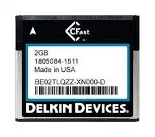
BE02TLQZZ-XN000-D
Flash Memory Card, SLC, CFast F200 Series
⚠️ Reference pricing provided. In case of supply shortages, we will connect you with our trusted procurement partners to ensure your project's continuity.
- Manufacturer: DELKIN DEVICES
- Product type: Flash Memory Cards
- Product Range: CFast F200 Series
| Delivery and price | |
|---|---|
| Units per pack | 50 |
| Price | 63.49 € |
| Current stock | 10+ |
| Lead time | 30 days |
Datasheet

CFast Embedded Flash Module – Gen II

401-0047-00 Rev A.

# **CFast™ Embedded Flash Module Gen II**

## **Engineering Specification**

**Document Number: 401-0047-00**

**Revision: A**

**32GB 1014765 – 1530 Made in USA BE32MGGZZ-XN000-D** al

© 2015 | Delkin Devices Inc.

**1**

CFast Embedded Flash Module – Gen II

401-0047-00 Rev A.

## **Table of Contents**

**1 General Specifications .................................................................................. 4** 1.1 Interfaces .................................................................................................. 6 Electrical / Physical Interfaces................................................................... 6 Controller Features ................................................................................... 6 1.2 Part Number Availability & Performance ................................................... 6 **2 Endurance ...................................................................................................... 7 3 Electrical Specifications ............................................................................... 8** 3.1 Pin and Signal Assignments ..................................................................... 8 3.2 Host Write Protection Schematic............................................................... 9 3.3 Supply Voltage ........................................................................................ 10 3.4 Power Consumption ................................................................................ 10 **4 Command Descriptions .............................................................................. 11** 4.1 Supported ATA Commands .................................................................... 11 4.2 Identify Device Data ................................................................................ 13 **5 SMART Functionality .................................................................................. 16** 5.1 SMART Data Structure ........................................................................... 17 5.1.1 Spare Block Count Attribute ........................................................... 18 5.1.2 Spare Block Count Worst Chip Attribute Threshold ....................... 18 5.1.3 Erase Count Attribute ..................................................................... 19 5.1.4 Total ECC Errors Attribute.............................................................. 19 5.1.5 Correctable ECC Errors Attribute ................................................... 20 5.1.6 SATA CRC Errors Attribute ............................................................ 20 5.1.7 Total Number of Reads Attribute .................................................... 21 5.1.8 Power On Count Attribute .............................................................. 21 5.1.9 Total LBA’s Written Attribute .......................................................... 22 5.1.10 Total LBA’s Read Attribute ........................................................... 22 5.1.11 Anchor Block Status Attribute ....................................................... 23 5.1.12 Trim Status Attribute .................................................................... 23 5.2 SMART Read Attribute Thresholds ......................................................... 24 5.2.1 Spare Block Count Attribute Threshold .......................................... 25 5.2.2 Spare Block Count Worst Chip Attribute Threshold ....................... 25 5.2.3 Erase Count Attribute Threshold .................................................... 26 5.2.4 Total ECC Errors Attribute Threshold ............................................. 26 5.2.5 Correctable ECC Errors Attribute ................................................... 26 5.2.6 UDMA CRC Errors Attribute ........................................................... 26 5.2.7 Total Number of Reads Attribute .................................................... 26 5.2.8 Power On Count Attribute .............................................................. 27 5.2.9 Total LBAs Written Attribute ........................................................... 27 5.2.10 Total LBAs Read Attribute ............................................................ 27 5.2.11 Anchor Block Status Attribute ....................................................... 27 5.2.12 Trim Status Attribute .................................................................... 27 5.3 SMART Return Status ............................................................................. 28 5.4 SMART Read Log ................................................................................... 29

© 2015 | Delkin Devices Inc.

**2**

CFast Embedded Flash Module – Gen II

401-0047-00 Rev A.

5.5 SMART Write Log ................................................................................... 30 5.6 SMART Read Remap Data ..................................................................... 31 5.7 SMART Read Wear Level Data .............................................................. 32 **6 Mechanical Form Factor ............................................................................. 34** 6.1 Physical Dimensions ............................................................................... 35

## **List of Figures**

Figure 2. Schematic for Implementation of Write Protect on Enabled Devices ..... 9 Figure 3. CFast Embedded Module Mechanical Description .............................. 35 Figure 4. CFast Embedded Module Mechanical Dimensions ............................. 36

## **List of Tables**

Table 1. Specification Summary ........................................................................... 4 Table 2. Delkin CFast Embedded Module Capacities and Part Numbers ............. 6 Table 3. Endurance Estimates by Part Number .................................................... 7 Table 4. Power and Signal Pin-out........................................................................ 8 Table 5. Supply Voltage  ..................................................................................... 10 Table 6. Power Consumption .............................................................................. 10 Table 7. Supported ATA Commands .................................................................. 11 Table 8. Device Sector Data ............................................................................... 13 Table 9. Smart Feature Register Values ............................................................. 13 Table 10. Smart Data Structure............................................................................17 Table 11. CFast Embedded Module Physical Dimensions ................................. 36

© 2015 | Delkin Devices Inc.

**3**

CFast Embedded Flash Module – Gen II

401-0047-00 Rev A.

## **1 General Specifications**

Delkin’s Gen II Industrial CFast embedded drive combines solid state reliability in a compact form factor, with SATA connectivity for significant performance advantages over traditional hard disk drives. Manufactured to CFast 1.1 specifications established by the CompactFlash Association, the CFast embedded module is suited to embedded industrial applications where space is restricted. The utilization of a rugged, industrial controller delivers reliability and robustness in applications where unstable power and unique usage models will tax commercial grade cards.  The shock, vibration, and temperature ratings allow usage in extreme environments. The drives can achieve sustained read & write rates of up to 120 MB/s and feature storage capacities from 2GB to 128GB. Delkin’s CFast cards also support the ability to be placed in a write protected state.

**Table 1. Specification Summary**

|Specification|Value|
|---|---|
|Model number|See Table 2|
|Capacity|SLC: 2GB–64GB|
|Interface|SATA revision 2.6, compatible with SATA 1.5Gb/s<br>and 3.0Gb/sinterfacerates.|
|Form Factor|CFAST Type I<br>Conforms to CFast1.1Standard|
|Hot swappable|Yes|
|Environmental certifications|RoHS, ESD, and CE/FCC|
|Performance||
|Interface burst speed|1.5 or3.0 Gb/s|
|Sustained read & write speed<br>(configurationdependent)|Up to 120 MB/s|
|Reliability/Data Integrity||
|MTBF|>2,000,000 power on hours at 0 - 25°C<br>>300,000 poweron hours @ 60°C|
|Endurance|See table in Section 2|
|Power||
|Supplyvoltage (allowable)|3.3V±10%|
|Typical current<br>(configurationdependent– values arefor32GB):||
|Idle|80mA|
|Read|200 mA|
|Write|250 mA|


© 2015 | Delkin Devices Inc.

**4**

CFast Embedded Flash Module – Gen II

401-0047-00 Rev A.

|Environmental||
|---|---|
|Storage temperature (°C)|-50~100°C|
|Operating temperature (°C)|-40~85°C|
|Relativehumidity (non-condensing)|95% under55°C|
|Vibration (operating/non-operating)|7.7GRMS<br>20Hz – 1000Hz @ 0.04 G2/Hz,<br>1000Hz–2000Hz @ 0.01 G2/Hz|
|Shock (operating/non-operating)|1,500G/0.5 ms|
|Acousticnoise|0 dB|
|Altitude|80,000feetmax.|
|Physical Dimensions||
|Height|3.6 mm|
|Width|42.8mm|
|Length|36.4 mm|


© 2015 | Delkin Devices Inc.

**5**

CFast Embedded Flash Module – Gen II

401-0047-00 Rev A.

## **1.1 Interfaces**

## **Electrical / Physical Interfaces**

- SATA Interface—supports SATA 1.5Gbps and 3Gbps interface

- Flash IO—Asynchronous Flash (3.3V)

## **Controller Features**

- **SATA II**

   - SATA Revision 2.6 compliant

   - Compatible with SATA 1.5Gbps and 3Gbps interface

## **1.2 Part Number Availability & Performance**

Delkin CFast embedded Solid State Drives are available in the capacities shown in the table below. Drives are also available with optional conformal coating for greater protection in extreme environments.

**Table 2. Delkin CFast Embedded Module Part Numbers & Performance**

|Capacity|Product Type|Standard Part<br>Number|Seq. Read Speed<br>Seq. Write Speed|
|---|---|---|---|
|2GB|SLC Industrial (-40 to 85°C)|BE02TLQZZ-XN000-D|30 MB/s<br>21 MB/s|
|4GB|SLC Industrial (-40 to 85°C)|BE04TGPZZ-XN000-D|40 MB/s<br>30 MB/s|
|8GB|SLC Industrial (-40 to 85°C)|BE08TGPZZ-XN000-D|61 MB/s<br>46 MB/s|
|16GB|SLC Industrial (-40 to 85°C)|BE16TGPZZ-XN000-D|95 MB/s<br>88 MB/s|
|32GB|SLC Industrial (-40 to 85°C)|BE32MGGZZ-XN000-D|105 MB/s<br>114 MB/s|
|64GB|SLC Industrial (-40 to 85°C)|BE64MGMZZ-XN000-D|120 MB/s<br>120 MB/s|


*Note: Usable capacities are within 10% of the gross capacity figures shown above, which is typical with all  NAND flash devices, as a small portion of the total is needed for controller firmware and spare block reserves.

© 2015 | Delkin Devices Inc.

**6**

CFast Embedded Flash Module – Gen II

401-0047-00 Rev A.

## **2 Endurance**

## **Endurance**

The table below provides estimates of drive endurance (expressed as Terabytes Written or TBW) based on specific workload scenarios, using a theoretical model that takes into account the specific flash specifications in each drive configuration. Contact Delkin for endurance estimates for other specific workload scenarios.

**Table 3. Endurance Estimates by Part Number**

|||Sequential Write,<br>24/7 Operation|
|---|---|---|
|Part Number(s)|Description|8KBytes/Sec|
|BE02TLQZZ-XN000-D|2GB SLC, Industrial Grade|117 TBW|
|BE04TGPZZ-XN000-D|4GB SLC, Industrial Grade|234 TBW|
|BE08TGPZZ-XN000-D|8GB SLC, Industrial Grade|468 TBW|
|BE16TGPZZ-XN000-D|16GB SLC, Industrial Grade|937 TBW|
|BE32MGGZZ-XN000-D|32GB SLC, Industrial Grade|1875 TBW|
|BE64MGMZZ-XN000-D|64GB SLC, Industrial Grade|3750 TBW|


The figures provided are estimates and not guarantees of endurance.  Actual results may vary depending on usage, operating temperature and other conditions.

© 2015 | Delkin Devices Inc.

**7**

CFast Embedded Flash Module – Gen II

401-0047-00 Rev A.

## **3 Electrical Specifications**

## **3.1 Pin and Signal Assignments**

**Table 4. Power and Signal Pin-out**

|Pin #|CFAST|<br>Description|
|---|---|---|
|S1|SGND|Signal Ground|
|S2|A+|SATA PAIR A|
|S3|A-||
|S4|SGND|Digital GND|
|S5|B-|SATA PAIR B|
|S6|B+||
|S7|SGND|Signal Ground|
|Key|||
|Key|||
|PC1|CDI|Card Detect In|
|PC2|GND|Ground|
|PC3|NC|No Connect|
|PC4|NC|No Connect|
|PC5|NC|No Connect|
|PC6|NC|No Connect|
|PC7|GND|Ground|
|PC8|LED1|LED Output|
|PC9|LED2|LED Output|
|PC10|IO1|Reserved(Write Protect,if enabled)|
|PC11|IO2|Reserved|
|PC12|IO3|Reserved|
|PC13|3.3V|Power|
|PC14|3.3V|Power|
|PC15|GND|Ground|
|PC16|GND|Ground|
|PC17|CDO|Card Detect Out|


© 2015 | Delkin Devices Inc.

**8**

CFast Embedded Flash Module – Gen II

401-0047-00 Rev A.

## **3.2 Host Write Protection Schematic**

**Figure 1. Schematic for Implementation of Write Protection on Enabled Devices**

© 2015 | Delkin Devices Inc.

**9**

CFast Embedded Flash Module – Gen II

401-0047-00 Rev A.

## **3.3 Supply Voltage**

## **Table 5. Supply Voltage**

|Parameter|Rating|
|---|---|
|Operating Voltage|3.3V|


## **3.4 Power Consumption**

**Table 6. Power Consumption Max Figures**

|Part Number|Capacity|Idle (mA)|Read (mA)|Write (mA)|
|---|---|---|---|---|
|BE02TLQZZ-XN000-D|2GB|80|110|120|
|BE04TGPZZ-XN000-D|4GB|80|130|150|
|BE08TGPZZ-XN000-D|8GB|80|140|170|
|BE16TGPZZ-XN000-D|16GB|80|170|240|
|BE32MGGZZ-XN000-D|32GB|80|150|200|
|BE64MGMZZ-XN000-D|64GB|80|200|250|


© 2015 | Delkin Devices Inc.

**10**

CFast Embedded Flash Module – Gen II

401-0047-00 Rev A.

## **4 Command Descriptions**

## **4.1 Supported ATA Commands**

The commands listed in the following table are supported by the CFast embedded MODULE.

## **Table 7. Supported ATA Commands**

|Command Name|Command<br>Code Hex)|FR|SC|SN|CY|DR|FR|LBA|
|---|---|---|---|---|---|---|---|---|
|Check Power Mode|E5hor98h|-|-|-|-|Y|-|-|
|Data SetManagement|06h|-|Y|-|-|Y|-|-|
|DownloadMicrocode|92h|Y|Y|Y|-|Y|-|-|
|ExecuteDriveDiagnostic|90h|-|-|-|-|-|-|-|
|FlushCache|E7h|-|-|-|-|Y|-|-|
|FlushCacheExt|Eah|-|-|-|-|Y|-|-|
|format track|50h|-|Y|-|Y|Y|Y|Y|
|IdentifyDevice|ECh|-|-|-|-|Y|-|-|
|Idle|E3hor97h|-|-|Y|-|Y|-|-|
|IdleImmediate|E1hor95h|-|-|-|-|Y|-|-|
|InitializeDriveParameters|91h|-|Y|-|-|Y|Y|-|
|MediaLock|DEh|-|-|-|-|Y|-|-|
|Media Unlock|DFh|-|-|-|-|Y|-|-|
|NOP|00h|-|-|-|-|Y|-|-|
|ReadBuffer|E4h|-|-|-|-|Y|-|-|
|ReadDMA|C8horC9h|-|Y|Y|Y|Y|Y|Y|
|ReadDMA Ext|25h|-|Y|Y|Y|Y|-|Y|
|ReadFPDMAQueued|60h|Y|Y|Y|Y|Y|-|Y|
|ReadLogExt|2Fh|-|Y|Y|Y|Y|-|Y|
|ReadMultiple|C4h|-|Y|Y|Y|Y|Y|Y|
|ReadMultipleExt|29h|-|Y|Y|Y|Y|-|Y|
|ReadNativeMax Address|F8h|-|-|-|-|Y|-|-|
|ReadNativeMax AddressExt|27h|-|-|-|-|Y|-|-|
|Read Sector(s)|20hor 21h|-|Y|Y|Y|Y|Y|Y|
|Read Sector(s)Ext|24h|-|Y|Y|Y|Y|-|Y|
|ReadVerify Sector(s)|40h|-|Y|Y|Y|Y|Y|Y|
|ReadVerify Sector(s)Ext|42h|-|Y|Y|Y|Y|-|Y|
|Recalibrate|1Xh|-|-|-|-|Y|-|-|
|SanitizeDevice|B4h|-|-|-|-|Y|-|-|
|SecurityDisablePassword|F6h|-|-|-|-|Y|-|-|
|SecurityErasePrepare|F3h|-|-|-|-|Y|-|-|
|SecurityErase Unit|F4h|-|-|-|-|Y|-|-|
|SecurityFreezeLock|F5h|-|-|-|-|Y|-|-|
|Security SetPassword|F1h|-|-|-|-|Y|-|-|
|Security Unlock|F2h|-|-|-|-|Y|Y|-|
|Seek|7Xh|-|-|Y|Y|Y|Y|Y|
|SetFeature|EFh|Y|-|-|-|Y|-|-|
|SetMax Address|F9h|-|Y|Y|Y|Y|Y|Y|
|SetMax AddressExt|37h|-|Y|Y|Y|Y|-|Y|
|SetMultipleMode|C6h|-|Y|-|-|Y|-|-|
|Set SleepMode|E6hor99h|-|-|-|-|Y|-|-|


© 2015 | Delkin Devices Inc.

**11**

CFast Embedded Flash Module – Gen II

401-0047-00 Rev A.

|SMART Disable Operations|B0h|Y|Y|-|Y|Y|-|-|
|---|---|---|---|---|---|---|---|---|
|SMART Enable Operations|B0h|Y|Y|-|Y|Y|-|-|
|SMART Enable/DisableAutosave|B0h|Y|Y|-|Y|Y|-|-|
|SMART Execute Off-LineImmediate|B0h|Y|Y|-|Y|Y|-|-|
|SMART ReadData|B0h|Y|Y|-|Y|Y|-|-|
|SMART ReturnStatus|B0h|Y|Y|-|Y|Y|-|-|
|Standby|E2hor96h|-|Y|-|-|Y|-|-|
|StandbyImmediate|E0hor94h|-|-|-|-|Y|-|-|
|WriteBuffer|E8h|-|-|-|-|Y|-|-|
|WriteDMA|CAhorCBh|-|Y|Y|Y|Y|Y|Y|
|WriteDMA Ext|35h|-|Y|Y|Y|Y|-|Y|
|WriteFPDMAQueued|61h|Y|Y|Y|Y|Y|-|Y|
|WriteLogExt|3Fh|-|Y|Y|Y|Y|-|Y|
|WriteMultiple|C5h|-|Y|Y|Y|Y|Y|Y|
|WriteMultipleExt|39h|-|Y|Y|Y|Y|-|Y|
|Write Sector(s)|30hor31h|-|Y|Y|Y|Y|Y|Y|
|Write Sector(s)Ext|34h|-|Y|Y|Y|Y|-|Y|
|WriteVerify|3Ch|-|Y|Y|Y|Y|Y|Y|


## Notes:

FR: Feature Register SC: Sector Count Register SN:  Sector Number Register CY: Cylinder Low/High Register DR: Drive bit of Drive/Head Register HD: Head No. (0 to 15) of Drive/Head Register LBA: LBA bit of Drive/Head Register Y: Used for the command

- -: Not used for the command

© 2015 | Delkin Devices Inc.

**12**

CFast Embedded Flash Module – Gen II

401-0047-00 Rev A.

## **4.2 Identify Device Data**

The following table details the information returned by the `IDENTIFY DEVICE` ATA command.

## **Table 8. Device Sector Data**

|**Word**|**Default Value**|**Bytes**|**Description**|
|---|---|---|---|
|0|045Ah|2|General configuration bit-significant information(-id)|
|1|XXXXh|2|Default number of cylinders|
|2|0000h|2|Reserved|
|3|00XXh|2|Default number of heads|
|4|0000h|2|Number of unformatted bytesper track|
|5|0200h|2|Number of unformatted bytesper sector|
|6|XXXXh|2|Default number of sectorsper track|
|7-8|XXXXh|4|Number of sectorsper card|
|9|0000h|2|Reserved|
|10-19|XXXXh|20|Serial number(20 ASCII characters)|
|20|0002h|2|Buffer type(dual-ported multi-sector)|
|21|0001h|2|Buffer size in 512 byte increments|
|22|0004h|2|# ECC bytespassed on Read/Write LongCommands|
|23-26|XXXXh|8|Firmware revision(8 ASCII characters)|
|27-46|XXXXh|40|Model number(40 ASCII characters)|
|47|8001h|2|Maximum 1 sector on Read/Write Multiple command|
|48|0000h|2|Double Word Not Supported|
|49|0F00h|2|Capabilities: DMA, LBA, IORDY supported|
|50|4001h|2|Capabilities: device specific standbytimer minimum|
|51|0200h|2|PIO data transfer cycle timingmode 2|
|52|0000h|2|DMA data transfer cycle timingmode not supported|
|53|0007h|2|Data fields 54 to 58, 64 to 70 and 88 are valid|
|54|XXXXh|2|Number of current logical cylinders|
|55|XXXXh|2|Number of current logical heads|
|56|XXXXh|2|Number of current logical sectorsper track|
|57-58|XXXXh|4|Current capacityin sectors|
|59|D10Xh|2|Multiple sector setting is valid, Sanitize Device feature set, Block<br>Erase Ext,Overwrite Ext supported|
|60-61|XXXXh|4|Total number of addressable sectors in LBA mode|
|62|0000h|2|Single word DMA transfer not implemented|
|63|0X07h|2|Multi-word DMA transfer mode, modes 0, 1, 2 supported|
|64|0003h|2|Advanced PIO modes, modes 3 and 4 supported|
|65|0078h|2|Minimum Multiword DMA cycle time, 0 if no MDMA|
|66|0078h|2|Recommended Multiword DMA cycle time, 0 if no MDMA|
|67|0078h|2|Minimum PIO cycle time without flow control|


© 2015 | Delkin Devices Inc.

**13**

CFast Embedded Flash Module – Gen II

401-0047-00 Rev A.

|**Word**|**Default Value**|**Bytes**|**Description**|
|---|---|---|---|
|68|0078h|2|Minimum PIO cycle time with flow control|
|69|8000h|2|CFast specification not supported|
|70-74|0000h|10|Reserved|
|75|001Fh|2|Queue depth 32 for NCQ|
|76|0306h|2|SATA capabilities: SATA Gen 1 & Gen II, NCQ, host initiated power<br>management requests supported|
|77-79|0000h|6|Reserved|
|80|01E0h|2|Major Version Number, ATA-5 to ATA-8 support|
|81|FFFFh|2|Minor Version Number, not reported|
|82|742Bh|2|Command set: NOP, READ BUFFER, WRITE BUFFER, HPA,<br>volatile write cache, power management feature set, Security Mode<br>feature set, SMART feature set|
|83|7501h|2|Command set: FLUSH CACHE, FLUSH CACHE EXT, LBA48,<br>HPA SecurityExtensions,DOWNLOAD MICROCODE|
|84|4120H|2|Command set/feature supported extension:  World Wide Name,<br>General Purpose Logging|
|85|74XXh|2|Command set enabled: NOP, READ BUFFER, WRITE BUFFER,<br>HPA, volatile write cache enabled/disabled, power management<br>feature set, Security Mode feature set enabled/disabled, SMART<br>feature set enabled/disabled|
|86|BX01h|2|Command set enabled: FLUSH CACHE, FLUSH CACHE EXT,<br>LBA48,DOWNLOAD MICROCODE,words 119…120 valid|
|87|4120h|2|Command set/feature default|
|88|XX7Fh|2|Ultra DMA Mode, modes 0 - 6 supported|
|89|0000h|2|Time required for securityerase unit not specified|
|90|0000h|2|Time required for Enhanced securityerase unit not specified|
|91|0000h|2|Reserved|
|92|XXXXh|2|Master Password Revision Code|
|93-99|0000h|14|Reserved|
|100-103|XXXXh|8|Total number of sectors addressable in LBA48 mode|
|104|0000h|2|Reserved|
|105|0001h|2|Number of sectorsper Data Set Management command|
|106-107|0000h|4|Reserved|
|108-111|XXXXh|8|World Wide Name|
|112-118|0000h|14|Reserved|
|119|4000h|2|Command set/Feature set Supported extension|
|120|4000h|2|Command set/Feature Enabled extension|
|121-127|0000h|14|Reserved|
|128|0XXXh|2|Securitystatus|


© 2015 | Delkin Devices Inc.

**14**

CFast Embedded Flash Module – Gen II

401-0047-00 Rev A.

|**Word**|**Default Value**|**Bytes**|**Description**|
|---|---|---|---|
|129|XX00h|2|Write Protect status<br>Bit 15 = permanent write protect, out of spare blocks<br>Bit 14 = permanent write protect, due to table corruption<br>Bit 13 = read protection due to table corruption<br>Bit 9  =  permanent write protect from vendor command<br>Bit 8=temporarywrite protectfrom vendorcommand|
|130-133|XXXXh|8|Firmware date string|
|134-135|XXXXh|4|Firmware minor revision number|
|136-141|XXXXh|12|Firmware file name|
|142-147|XXXXh|12|Preformat file name|
|148-153|XXXXh|12|Anchorprogram file name|
|154-158|0000h|10|Reserved|
|159|A2XXh|2|Controller major and minor revision number|
|160|0000h|2|CF feature set and CFApower modes not supported|
|161|8001h|2|CFast specific support: PHYSLP mode supported|
|162|0000h|2|KeyManagement schemes: CPRM not supported|
|163|0000h|2|CFA advanced modes: not relevant for CFast|
|164|0000h|2|CFA advanced modes: not relevant for CFast|
|165-168|0000h|8|Reserved|
|169|0001h|2|Trim bit in Data Set Management supported|
|170-216|0000h|94|Reserved|
|217|0001h|2|Solid State Device(non-rotatingmedia)|
|218-221|0000h|8|Reserved|
|222|101Fh|2|Transport major version: Serial transport, SATA rev 2.6|
|223|FFFFh|2|Transport minor version: not reported|
|224-254|0000h|62|Reserved|
|255|XXA5h|2|Integrityword(Checksum and Signature)|


© 2015 | Delkin Devices Inc.

**15**

CFast Embedded Flash Module – Gen II

401-0047-00 Rev A.

## **5 SMART Functionality**

Delkin Devices Industrial CFast cards support the following SMART commands, determined by the Feature Register value.

## **Table 9: SMART Feature Register Values**

|Value|Command|
|---|---|
|D0h|SMART Read Data|
|D1h|SMART Read Attribute Thresholds|
|D2h|SMART Enable / Disable Attribute Autosave|
|D5h|SMART Read Log|
|D6h|SMART Write Log|
|D8h|SMART Enable Operations|
|D9h|SMART Disable Operations|
|DAh|Return Status|
|E0h|SMART Read Remap Data|
|E1h|SMART Read Wear Level Data|


SMART commands with Feature Register values not mentioned in the above table are not supported and will be aborted.

© 2015 | Delkin Devices Inc.

**16**

CFast Embedded Flash Module – Gen II

401-0047-00 Rev A.

## **5.1 SMART Data Structure**

The following 512 bytes make up the device SMART data structure. Users can obtain the data using the “Read Data” command (D0h.)

**Table 10. Smart Data Structure**

|Byte|Value|Description|
|---|---|---|
|0 – 1|0010h|SMART structure version|
|2 – 361||Attribute entries 1 to 30 (12 bytes each)|
|362|00h|Off-line data collection status  (no off-line data collection)|
|363|00h|Self-test execution status byte (self-test completed)|
|364 – 365|0000h|Total time in seconds to complete off-line data collection activity|
|366|00h|Vendor specific|
|367|00h|Off-line data collection capability (no off-line data collection)|
|368 – 369|0003h|SMART capability|
|370|00h|Error logging capability (no error logging)|
|371|00h|Vendor specific|
|372|00h|Short self-test routine recommended polling time (in minutes)|
|373|00h|Extended self-test routine recommended polling time (in minutes)|
|374 – 385|00h|Reserved|
|386 – 387|0004h|SMART Structure Version|
|388 – 391||Firmware “Commit” Counter|
|392 - 395||Firmware Wear Level Threshold|
|396||Global Wear Leveling Active|
|397||Global Bad Block Management active (returns 0 if bad block management is<br>still at local chip level, and returns 1 if global bad block management has<br>begun.)|
|398 – 401||Average Flash Block Erase Count|
|402 – 405||Number of Flash Blocks involved in the Wear Leveling|
|406 – 409||Number of total ECC errors during firmware initialization|
|410 – 413||Number of correctable ECC errors during firmware initialization|
|414 – 510|00h|Vendor specific|
|511||Data structure checksum|


© 2015 | Delkin Devices Inc.

**17**

CFast Embedded Flash Module – Gen II

401-0047-00 Rev A.

## **5.1.1 Spare Block Count Attribute**

This attribute gives information about the amount of available spare blocks.

|Offset|Value|Description|
|---|---|---|
|0|196|Attribute ID – Reallocation Count|
|1 – 2|0003h|Flags – Pre-fail type, attribute value is updated during normal<br>operation|
|3||Attribute value.  The value returned here is the percentage of<br>remaining spare blocks summed over all flash chips, i.e.<br>(100 x current spare blocks / initial spare blocks)|
|4||Attribute value (worst value)|
|5 – 7||Sum of the initial number of spare blocks for all flash chips|
|8 – 10||Sum of the current number of spare blocks for all flash chips|
|11|00h|Reserved|


This attribute is used for the SMART Return Status command.  If the attribute value field is less than the spare block threshold (set with the –tsbc preformat option), the SMART Return Status command will indicate a threshold exceeded condition.

## **5.1.2 Spare Block Count Worst Chip Attribute Threshold**

This attribute gives information about the amount of available spare blocks on the flash chip that has the lowest current number of spare blocks.

|Offset|Value|Description|
|---|---|---|
|0|213|Attribute ID – Spare Block Count Worst Chip (vendor specific)|
|1 – 2|0002h|Flags – Advisory type, attribute value is updated during normal<br>operation|
|3|64h|Attribute value.  This value is fixed at 100.|
|4|64h|Attribute value (worst value)|
|5 – 7||Initial number of spare blocks for the flash chip with the lowest current<br>number of spare blocks.|
|8 – 10||Current number of spare blocks for the flash chip with the lowest<br>current number of spare blocks.|
|11|00h|Reserved|


© 2015 | Delkin Devices Inc. **18**

CFast Embedded Flash Module – Gen II

401-0047-00 Rev A.

## **5.1.3 Erase Count Attribute**

This attribute gives information about the amount of flash block erases that have been performed.

|Offset|Value|Description|
|---|---|---|
|0|229|Attribute ID – Erase Count Usage (vendor specific)|
|1 – 2|000Xh|Flags – Pre-fail or Advisory type, attribute value is updated during<br>normal operation|
|3||Attribute value.  The value returned here is an estimation of the<br>remaining card life, in percent, based on the number of flash block<br>erases compared to the target number of erase cycles per block.|
|4||Attribute value (worst value)|
|5 - 10||Estimated total number of block erases.|
|11|00h|Reserved|


This attribute is used for the SMART Return Status command.  If the attribute value field is less than the erase count threshold (set with the –tec preformat option), the SMART Return Status command will indicate a threshold exceeded condition.

The target number of erase cycles per flash block is taken from the –mbec preformat option, or if this option is absent, from the MaxBlockEraseCount column in the Device Description file. The attribute type (pre-fail or advisory) can be set with the –ecwl preformat option.

## **5.1.4 Total ECC Errors Attribute**

This attribute gives information about the total number of ECC errors that have occurred on flash read commands during firmware runtime.  This attribute is not used for the SMART Return Status command.

|Offset|Value|Description|
|---|---|---|
|0|203|Attribute ID – Number of ECC Errors|
|1 – 2|0002h|Flags – Advisory type, attribute value is updated during normal operation|
|3|64h|Attribute value.  This value is fixed at 100.|
|4|64h|Attribute value (worst value)|
|5 – 8||Total number of ECC errors (correctable and uncorrectable)|
|9 – 10||---|
|11|00h|Reserved|


© 2015 | Delkin Devices Inc.

**19**

CFast Embedded Flash Module – Gen II

401-0047-00 Rev A.

## **5.1.5 Correctable ECC Errors Attribute**

This attribute gives information about the total number of correctable ECC errors that have occurred on flash read commands during firmware runtime.  This attribute is not used for the SMART Return Status command.

|Offset|Value|Description|
|---|---|---|
|0|204|Attribute ID – Number of corrected ECC Errors|
|1 – 2|0002h|Flags – Advisory type, attribute value is updated during normal operation|
|3|64h|Attribute value.  This value is fixed at 100.|
|4|64h|Attribute value (worst value)|
|5 – 8||Total number of correctable ECC errors|
|9 - 10||---|
|11|00h|Reserved|


## **5.1.6 SATA CRC Errors Attribute**

This attribute gives information about the total number of SATA CRC errors that have occurred on flash read commands.  This attribute is not used for the SMART Return Status command.

|Offset|Value|Description|
|---|---|---|
|0|199|Attribute ID – SATA CRC error rate|
|1 – 2|0002h|Flags – Advisory type, attribute value is updated during normal operation|
|3|64h|Attribute value.  This value is fixed at 100.|
|4|64h|Attribute value (worst value)|
|5 – 8||Total number of SATA CRC errors|
|9 – 10||---|
|11|00h|Reserved|


© 2015 | Delkin Devices Inc.

**20**

CFast Embedded Flash Module – Gen II

401-0047-00 Rev A.

## **5.1.7 Total Number of Reads Attribute**

This attribute gives information about the total number of flash read commands. This can be useful for interpretation of the number of correctable or total ECC errors.  This attribute is not used for the SMART Return Status command.

|Offset|Value|Description|
|---|---|---|
|0|232|Attribute ID – Number of Reads (vendor specific)|
|1 – 2|0002h|Flags – Advisory type, attribute value is updated during normal operation|
|3|64h|Attribute value.  This value is fixed at 100.|
|4|64h|Attribute value (worst value)|
|5 – 10||Total number of flash read commands|
|11|00h|Reserved|


## **5.1.8 Power On Count Attribute**

|**5.1.8**|**Power On**|**Count Attribute**|
|---|---|---|
|Offset|Value|Description|
|0|12|Attribute ID – Power On Count|
|1 – 2|0002h|Flags – Advisory type, attribute value is updated during normal operation|
|3|64h|Attribute value.  This value is fixed at 100.|
|4|64h|Attribute value (worst value)|
|5 – 8||Number of Power On cycles|
|9 – 10||---|
|11|00h|Reserved|


© 2015 | Delkin Devices Inc.

**21**

CFast Embedded Flash Module – Gen II

401-0047-00 Rev A.

## **5.1.9 Total LBA’s Written Attribute**

This attribute gives the total amount of data written to the disk, in units of 32MB (65536 sectors.)  This number can be converted to Terabytes written (TBW) by dividing the raw attribute value by 2[31] .

|Offset|Value|Description|
|---|---|---|
|0|241|Attribute ID – Total LBA’s Written (vendor specific)|
|1 – 2|0002h|Flags – Advisory type, attribute value is updated during normal operation|
|3|64h|Attribute value.  This value is fixed at 100.|
|4|64h|Attribute value (worst value)|
|5 – 10||Total number of LBA’s written to the disk, divided by 65536|
|11|00h|Reserved|


## **5.1.10 Total LBA’s Read Attribute**

This attribute gives the total amount of data read from the disk, in units of 32MB (65536 sectors.)  This number can be converted to Terabytes read (TBW) by dividing the raw attribute value by 2[31] .

|Offset|Value|Description|
|---|---|---|
|0|242|Attribute ID – Total LBA’s Read (vendor specific)|
|1 – 2|0002h|Flags – Advisory type, attribute value is updated during normal operation|
|3|64h|Attribute value.  This value is fixed at 100.|
|4|64h|Attribute value (worst value)|
|5 – 10||Total number of LBA’s read from the disk, divided by 65536|
|11|00h|Reserved|


© 2015 | Delkin Devices Inc.

**22**

CFast Embedded Flash Module – Gen II

401-0047-00 Rev A.

## **5.1.11 Anchor Block Status Attribute**

This attribute reports how many times the Anchor Block of the card has been re-written, either by the Anchor Block repair routine or by a firmware update.

|Anchor Block|repair routine or|by a firmware update.|
|---|---|---|
|Offset|Value|Description|
|0|214|Attribute ID – Anchor Block Status (vendor specific)|
|1 – 2|0002h|Flags – Advisory type, attribute value is updated during normal operation|
|3|64h|Attribute value.  This value is fixed at 100.|
|4|64h|Attribute value (worst value)|
|5 – 8||Anchor Block Write Count|
|9 – 10||---|
|11|00h|Reserved|


## **5.1.12 Trim Status Attribute**

This attribute gives percent ratio for the disk space that is currently in the trimmed state, reported as the attribute value.  The range for the attribute value is 1 to 99, and does not reach 100 even for a fully trimmed card since the management blocks are also counted, which do not have trim status.

|Offset|Value|Description|
|---|---|---|
|0|215|Attribute ID – Trim Status (vendor specific)|
|1 – 2|0002h|Flags – Advisory type, attribute value is updated during normal operation|
|3|64h|Attribute value.|
|4|64h|Attribute value (worst value)|
|5 – 10||---|
|11|00h|Reserved|


© 2015 | Delkin Devices Inc.

**23**

CFast Embedded Flash Module – Gen II

401-0047-00 Rev A.

## **5.2 SMART Read Attribute Thresholds**

COMMAND CODE – B0h with a Feature Register value of D1h

PROTOCOL – PIO  data in

INPUTS -

|INPUTS -|||||||||
|---|---|---|---|---|---|---|---|---|
|Register|7|6|5|4|3|2|1|0|
|Features|D1h||||||||
|Sector Count|||||||||
|Sector Number|||||||||
|Cylinder Low|4Fh||||||||
|Cylinder High|C2h||||||||
|Device /Head|1|1|1|D|||||
|Command|B0h||||||||


## NORMAL OUTPUTS – None required

ERROR OUTPUTS – Aborted if either the signature in the Cylinder registers is invalid or if SMART is not enabled.

DESCRIPTION – This command returns one sector of SMART attribute thresholds.  The data structure returned is:

|Offset|Value|Description|
|---|---|---|
|0- 1|0010h|SMARTstructureversion|
|2 –361||Attribute threshold entries1to 30 (12bytes each)|
|362 –379|00h|Reserved|
|380–510|00h|----|
|511||Data structure checksum|


© 2015 | Delkin Devices Inc.

**24**

CFast Embedded Flash Module – Gen II

401-0047-00 Rev A.

## **5.2.1 Spare Block Count Attribute Threshold**

COMMAND CODE – B0h with a Feature Register value of D1h

PROTOCOL – PIO  data in

INPUTS -

|INPUTS -|||||||||
|---|---|---|---|---|---|---|---|---|
|Register|7|6|5|4|3|2|1|0|
|Features|D1h||||||||
|Sector Count|||||||||
|Sector Number|||||||||
|Cylinder Low|4Fh||||||||
|Cylinder High|C2h||||||||
|Device /Head|1|1|1|D|||||
|Command|B0h||||||||


## NORMAL OUTPUTS – None required

ERROR OUTPUTS – Aborted if either the signature in the Cylinder registers is invalid or if SMART is not enabled.

DESCRIPTION – This command returns one sector of SMART attribute thresholds.  The data structure returned is:

|Offset|Value|Description|
|---|---|---|
|0- 1|0010h|SMARTstructureversion|
|2 –361||Attribute threshold entries1to 30 (12bytes each)|
|362 –379|00h|Reserved|
|380–510|00h|----|
|511||Data structure checksum|


## **5.2.2 Spare Block Count Worst Chip Attribute Threshold**

|Offset|Value|Description|
|---|---|---|
|0|213|AttributeID –SpareBlockCountWorst Chip (vendorspecific)|
|1|00h|No thresholdforthe SpareBlockCountWorst ChipAttribute|
|2 – 11|00h|Reserved|


© 2015 | Delkin Devices Inc.

**25**

CFast Embedded Flash Module – Gen II

401-0047-00 Rev A.

## **5.2.3 Erase Count Attribute Threshold**

|Offset|Value|Description|
|---|---|---|
|0|229|AttributeID – Erase Count Usage (vendorspecific)|
|1||Erase CountThreshold as definedinperformat|
|2 – 11|00h|Reserved|


## **5.2.4 Total ECC Errors Attribute Threshold**

|Offset|Value|Description|
|---|---|---|
|0|203|AttributeID – Numberof ECC errors|
|1|00h|No thresholdfortheTotal ECCErrorsAttribute|
|2 – 11|00h|Reserved|


## **5.2.5 Correctable ECC Errors Attribute**

|Offset|Value|Description|
|---|---|---|
|0|204|AttributeID – NumberofcorrectedECC errors|
|1|00h|No thresholdforthe CorrectableECCErrorsAttribute|
|2 – 11|00h|Reserved|


## **5.2.6 UDMA CRC Errors Attribute**

|Offset|Value|Description|
|---|---|---|
|0|199|AttributeID –UDMACRC error rate|
|1|00h|No thresholdforthe UDMACRCErrorsAttribute|
|2 – 11|00h|Reserved|


## **5.2.7 Total Number of Reads Attribute**

|Offset|Value|Description|
|---|---|---|
|0|232|Attribute ID–Number of Reads (vendor specific)|
|1|00h|No threshold for the Total Number of Reads Attribute|
|2 – 11|00h|Reserved|


© 2015 | Delkin Devices Inc.

**26**

CFast Embedded Flash Module – Gen II

401-0047-00 Rev A.

## **5.2.8 Power On Count Attribute**

|Offset|Value|Description|
|---|---|---|
|0|12|AttributeID – PowerOnCount|
|1|00h|No thresholdforthePowerOnCountAttribute|
|2 – 11|00h|Reserved|


## **5.2.9 Total LBAs Written Attribute**

|Offset|Value|Description|
|---|---|---|
|0|241|AttributeID – Total LBAsWritten(vendorspecific)|
|1|00h|No thresholdfortheTotal LBAsWritten Attribute|
|2 – 11|00h|Reserved|


## **5.2.10 Total LBAs Read Attribute**

|Offset|Value|Description|
|---|---|---|
|0|242|AttributeID – Total LBAsRead (vendorspecific)|
|1|00h|No thresholdfortheTotal LBAsReadAttribute|
|2 – 11|00h|Reserved|


## **5.2.11 Anchor Block Status Attribute**

|Offset|Value|Description|
|---|---|---|
|0|214|AttributeID – Anchor BlockStatus (vendorspecific)|
|1|00h|No thresholdfortheAnchor BlockStatusAttribute|
|2 – 11|00h|Reserved|


## **5.2.12 Trim Status Attribute**

|Offset|Value|Description|
|---|---|---|
|0|215|Attribute ID–Trim Status (vendor specific)|
|1|00h|No threshold for the Trim Status Attribute|
|2 – 11|00h|Reserved|


© 2015 | Delkin Devices Inc.

**27**

CFast Embedded Flash Module – Gen II

401-0047-00 Rev A.

## **5.3 SMART Return Status**

COMMAND CODE – B0h with a Feature Register value of DAh

PROTOCOL –  non-data

INPUTS -

|INPUTS -|||||||||
|---|---|---|---|---|---|---|---|---|
|Register|7|6|5|4|3|2|1|0|
|Features|DAh||||||||
|Sector Count|||||||||
|Sector Number|||||||||
|Cylinder Low|4Fh||||||||
|Cylinder High|C2h||||||||
|Device /Head|1|1|1|D|||||
|Command|B0h||||||||


NORMAL OUTPUTS – Returns a status indication as described below.

ERROR OUTPUTS – Aborted if either the signature in the Cylinder registers is invalid or if SMART is not enabled.

DESCRIPTION – This command checks the device reliability status.  If a threshold exceeded condition exists for either the Spare Block Count attribute or the Erase Count attribute, the device will set the Cylinder Low register to F4h and the Cylinder High register to 2Ch.  If no threshold exceeded condition exists, the device will set the Cylinder Low register to F4h and the Cylinder High register to C2h.

© 2015 | Delkin Devices Inc.

**28**

CFast Embedded Flash Module – Gen II

401-0047-00 Rev A.

## **5.4 SMART Read Log**

COMMAND CODE – B0h with a Feature Register value of D5h

PROTOCOL – PIO data in.

INPUTS -

|INPUTS -|||||||||
|---|---|---|---|---|---|---|---|---|
|Register|7|6|5|4|3|2|1|0|
|Features|D5h||||||||
|Sector Count|Number of sectors to be read||||||||
|Sector Number|Log address||||||||
|Cylinder Low|4Fh||||||||
|Cylinder High|C2h||||||||
|Device / Head|1|1|1|D|||||
|Command|B0h||||||||


NORMAL OUTPUTS – None required.

ERROR OUTPUTS – Aborted if either the signature in the Cylinder registers, the Log address or the number of sectors is invalid, or if SMART is not enabled.

DESCRIPTION – This command will return data of the SMART log.  The following Log addresses are defined:

|Address|Description|
|---|---|
|0x00|LogDirectory|
|0x80–0x9F|HostVendorSpecificLogs|
|0xA0|SMART Wear Level Data|
|0xA1|SMART RemapData|
|0xA2|Reserved|


The Log Directory (at Log address 0) returns one sector that shows the number of sectors for Log addresses 1 to 255:

|Offset|Value|Description|
|---|---|---|
|0- 1|1|SMART LoggingVersion|
|256–319|16|Numberofsectorsinthelogs at addresses 0x80–0x9F|
|320–321|4|Numberofsectorsinthelogs at address 0xA0|
|322 –323|1|Numberofsectorsinthelogs at address 0xA1|
|324 –325|1|Numberofsectorsinthelogs at address 0xA2|


All other bytes in the Log Directory are zero.

The Host Vendor Specific Logs can be used by the host to store and retrieve arbitrary data.

© 2015 | Delkin Devices Inc.

**29**

CFast Embedded Flash Module – Gen II

401-0047-00 Rev A.

The SMART Wear Level Data and SMART Remap Data Logs return the same data that is also returned by the SMART Read Wear Level Data and SMART Read Remap Data commands.

## **5.5 SMART Write Log**

COMMAND CODE – B0h with a Feature Register value of D6h

PROTOCOL – PIO data out.

INPUTS -

|INPUTS -|||||||||
|---|---|---|---|---|---|---|---|---|
|Register|7|6|5|4|3|2|1|0|
|Features|D6h||||||||
|Sector Count|Number of sectors to be written||||||||
|Sector Number|Log address||||||||
|Cylinder Low|4Fh||||||||
|Cylinder High|C2h||||||||
|Device / Head|1|1|1|D|||||
|Command|B0h||||||||


## NORMAL OUTPUTS – None required.

ERROR OUTPUTS – Aborted if either the signature in the Cylinder registers, the Log address or the number of sectors is invalid, or if SMART is not enabled.

DESCRIPTION – This command can be used to write data into the SMART log (see section 6.4 for the definition of the log addresses.) Writes are allowed only to the Host Vendor Specific logs, all other log addresses can only be read.

© 2015 | Delkin Devices Inc.

**30**

CFast Embedded Flash Module – Gen II

401-0047-00 Rev A.

## **5.6 SMART Read Remap Data**

COMMAND CODE – B0h with a Feature Register value of E0h

PROTOCOL – PIO data in.

INPUTS -

|INPUTS -|||||||||
|---|---|---|---|---|---|---|---|---|
|Register|7|6|5|4|3|2|1|0|
|Features|E0h||||||||
|Sector Count|01h||||||||
|Sector Number|||||||||
|Cylinder Low|4Fh||||||||
|Cylinder High|C2h||||||||
|Device /Head|1|1|1|D|||||
|Command|B0h||||||||


## NORMAL OUTPUTS – None required.

ERROR OUTPUTS – Aborted if either the signature in the Cylinder registers is invalid, if the Sector Count is not 1, or if SMART is not enabled.

DESCRIPTION – This command returns one sector of spare block information.  The information is the initial number of blocks (directly after the preformat) per flash chip available for bad block remap, and the current number of blocks per flash chip available for bad block remap.  The layout of the returned sector is:

|sector is:||
|---|---|
|Offset|Description|
|0-31|Initial number of replacement blocks for chips 0–15, 2 bytes per entry|
|32–63|Current number of replacement blocks for chips 0–15, 2 bytes per entry|
|64 -511|----|


© 2015 | Delkin Devices Inc.

**31**

CFast Embedded Flash Module – Gen II

401-0047-00 Rev A.

## **5.7 SMART Read Wear Level Data**

COMMAND CODE – B0h with a Feature Register value of E1h

PROTOCOL – PIO data in.

INPUTS -

|INPUTS -|||||||||
|---|---|---|---|---|---|---|---|---|
|Register|7|6|5|4|3|2|1|0|
|Features|E1h||||||||
|Sector Count|04h||||||||
|Sector Number|||||||||
|Cylinder Low|4Fh||||||||
|Cylinder High|C2h||||||||
|Device /Head|1|1|1|D|||||
|Command|B0h||||||||


## NORMAL OUTPUTS – None required.

ERROR OUTPUTS – Aborted if either the signature in the Cylinder registers is invalid, if the Sector Count is not 4, or if SMART is not enabled.

DESCRIPTION – This command will return four sectors of information regarding the status of the wear leveling.  The information returned is the distribution of the blocks into the 1024 possible wear level classes.  The layout of the returned sector is:

|leveling.  The<br>classes.  The|information returned is the distribution of the blocks into the 1024 poss<br>layout of the returned sector is:|
|---|---|
|Offset|Description|
|0-3|Marker Bytes,fixedvalue 0xFFFFFFFF|
|4 –5|LowestWear LevelClass|
|6– 7|HighestWear LevelClass|
|8– 15|Wear LevelClass entry1|
|16– 23|Wear LevelClass entry2|
|24 –31|Wear LevelClass entry 3|
|….|….|
|2040- 2047|Wear LevelClass entry255|


Each Wear Level Class entry consists of this data:

|Offset|Description|
|---|---|
|0-3|Wear LevelClassIndex|
|4 – 7|NumberofblocksinthisWear LevelClass|


Unused Wear Level Class entries are zero.

A block moves from one wear level class into the next when it reaches the number of erases that is specified as the “Wear Level Threshold” in the preformat.  A common threshold number is 4095, this means that blocks in wear level class 0 have seen 0 to 4095 erases, blocks in wear level class 1 have

© 2015 | Delkin Devices Inc.

**32**

CFast Embedded Flash Module – Gen II

401-0047-00 Rev A.

seen 4096 to 8191 erases, and so on.  Using this information, statements about the wear of the card and of the estimated remaining life can be made.

© 2015 | Delkin Devices Inc.

**33**

CFast Embedded Flash Module – Gen II

401-0047-00 Rev A.

## **6 Mechanical Form Factor**

**Figure 2. CFast Embedded Module Mechanical Description**

© 2015 | Delkin Devices Inc.

**34**

CFast Embedded Flash Module – Gen II

401-0047-00 Rev A.

## **6.1 Physical Dimensions**

**Table 11. CFast Embedded Module Physical Dimensions**

|Dimension|Measurement|
|---|---|
|Height|3.6mm|
|Width|42.8mm|
|Length|36.4mm|


**Figure 3. CFast Embedded Module Mechanical Dimensions**

© 2015 | Delkin Devices Inc.

**35**
Updated at February 9, 2023
About Novapart
Novapart is a B2B electronic component broker specialising in stock shortages and cost reduction. We source hard-to-find parts and identify compliant alternatives across a catalogue of 410,000+ components from 500+ manufacturers.
Learn more →Stock Shortage Specialist
When a component is unavailable, discontinued or has an unacceptable lead time, we tap into our network of vetted European and Asian distributors to source what you need — without compromising on quality or traceability.
Request a quote →Compliant Alternatives
We identify pin-to-pin, electrically equivalent substitutes that meet the same certifications (RoHS, AEC-Q100, REACH) as your original specification — validated against datasheets, not just part numbers. Often at a lower cost.
BOM Analysis service →