
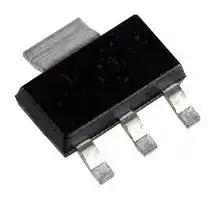


BCP56-10T3G
Bipolar (BJT) Single Transistor, NPN, 80 V, 1 A, 1.5 W, SOT-223, Surface Mount
- Manufacturer: ONSEMI
- Product type: Single Bipolar Junction Transistors - BJT
- SVHC: No SVHC (15-Jan-2018)
- No. of Pins: 4Pins
- Product Range: BCP56
- Qualification: -
- Power Dissipation: 1.5W
- Transistor Mounting: Surface Mount
- Transistor Polarity: NPN
- Transition Frequency: 130MHz
- Transistor Case Style: SOT-223
- DC Current Gain hFE Min: 63hFE
- Operating Temperature Max: 150°C
- Continuous Collector Current: 1A
- Collector Emitter Voltage Max: 80V
| Delivery and price | |
|---|---|
| Units per pack | 4000 |
| Price | 0.058 € |
| Current stock | 10+ |
| Lead time | 30 days |
**Share Feedback DATA SHEET** Your Opinion Matters **www.onsemi.com** ~~ee~~ ## NPN Silicon Epitaxial Transistor ## **MEDIUM POWER NPN SILICON HIGH CURRENT TRANSISTOR SURFACE MOUNT** ## BCP56 Series These NPN Silicon Epitaxial transistors are designed for use in audio amplifier applications. The device is housed in the SOT−223 package, which is designed for medium power surface mount applications. ## **Features** **==> picture [87 x 69] intentionally omitted <==** **----- Start of picture text -----**<br> COLLECTOR 2,4<br>BASE<br>1<br>EMITTER 3<br>**----- End of picture text -----**<br> - High Current: 1.0 A - The SOT−223 package can be soldered using wave or reflow. The formed leads absorb thermal stress during soldering, eliminating the possibility of damage to the die - Available in 12 mm Tape and Reel - Use BCP56T1G to Order the 7 inch/1000 Unit Reel - Use BCP56T3G to Order the 13 inch/4000 Unit Reel - PNP Complement is BCP53T1G - S and NSV Prefix for Automotive and Other Applications Requiring Unique Site and Control Change Requirements; AEC−Q101 Qualified and PPAP Capable - These Devices are Pb−Free, Halogen Free/BFR Free and are RoHS Compliant **MAXIMUM RATINGS** (TC = 25C unless otherwise noted) |**MAXIMUM RATINGS **(TC = 25C unless otherwise noted)C = 25C unless otherwise noted)= 25C unless otherwise noted)C unless otherwise noted)C unless otherwise noted)|(TC = 25C unless otherwise noted)C = 25C unless otherwise noted)= 25C unless otherwise noted)C unless otherwise noted)C unless otherwise noted)|(TC = 25C unless otherwise noted)C = 25C unless otherwise noted)= 25C unless otherwise noted)C unless otherwise noted)C unless otherwise noted)|| |---|---|---|---| |**Rating**|**Symbol**|**Value**|**Unit**| |Collector−Emitter Voltage|VCEO|80|Vdc| |Collector−Base Voltage|VCBO|100|Vdc| |Emitter−Base Voltage|VEBO|5|Vdc| |Collector Current|IC|1|Adc| |Collector Current − Peak (Note 1)|ICM|2|Adc| |Total Power Dissipation<br>@ TA= 25C (Note 2)<br>Derate above 25C|PD|1.5<br>12|W<br>mW/C| |Operating and Storage<br>Temperature Range|TJ, Tstg|−65 to 150|C| **==> picture [44 x 68] intentionally omitted <==** **----- Start of picture text -----**<br> % 4<br>1 2 3<br>SOT−223<br>CASE 318E<br>STYLE 1<br>**----- End of picture text -----**<br> ## **MARKING DIAGRAM** **==> picture [146 x 106] intentionally omitted <==** **----- Start of picture text -----**<br> AYW<br>XXXXX<br>1<br>XXXXX = Specific Device Code<br>A = Assembly Location<br>Y = Year<br>W = Work Week<br>= Pb−Free Package<br>(Note: Microdot may be in either location)<br>**----- End of picture text -----**<br> ## **ORDERING INFORMATION** See detailed ordering, marking and shipping information on page 5 of this data sheet. NOTE: Some of the devices on this data sheet have been **DISCONTINUED** . Please refer to the table on page 5. ## **THERMAL CHARACTERISTICS** |**THERMAL CHARACTERISTICS**|~~ee~~|~~es~~|| |---|---|---|---| |**Characteristic**<br>~~ee~~|**Symbol**<br>~~ee~~<br>~~ee~~|**Max**<br>~~ee~~<br>~~es~~|**Unit**<br>~~ee~~| |Thermal Resistance,<br>Junction−to−Ambient<br>(surface mounted)<br>~~PT~~|R JA<br>~~ee~~<br>~~PT~~|83.3<br>~~es~~<br>~~PT~~|C/W<br>~~PT~~| |Maximum Temperature for<br>Soldering Purposes<br>Time in Solder Bath<br>~~ee~~|TL<br>~~ee~~|260<br>10<br>~~ee~~|C<br>Sec<br>~~ee~~| Stresses exceeding those listed in the Maximum Ratings table may damage the device. If any of these limits are exceeded, device functionality should not be assumed, damage may occur and reliability may be affected. 1. Reference SOA curve. 2. Device mounted on a FR−4 glass epoxy printed circuit board 1.575 in x 1.575 in x 0.0625 in; mounting pad for the collector lead = 0.93 sq in. Publication Order Number: **1** Semiconductor Components Industries, LLC, 2016 **August, 2024 − Rev. 16** **BCP56T1/D** ## **BCP56 Series** **ELECTRICAL CHARACTERISTICS** (TA = 25C unless otherwise noted) |**ELECTRICAL CHARACTERISTICS **(TA = 25C unless otherwise noted)A = 25C unless otherwise noted)= 25C unless otherwise noted)C unless otherwise noted)C unless otherwise noted)|**ELECTRICAL CHARACTERISTICS **(TA = 25C unless otherwise noted)A = 25C unless otherwise noted)= 25C unless otherwise noted)C unless otherwise noted)C unless otherwise noted)|**ELECTRICAL CHARACTERISTICS **(TA = 25C unless otherwise noted)A = 25C unless otherwise noted)= 25C unless otherwise noted)C unless otherwise noted)C unless otherwise noted)|**ELECTRICAL CHARACTERISTICS **(TA = 25C unless otherwise noted)A = 25C unless otherwise noted)= 25C unless otherwise noted)C unless otherwise noted)C unless otherwise noted)|**ELECTRICAL CHARACTERISTICS **(TA = 25C unless otherwise noted)A = 25C unless otherwise noted)= 25C unless otherwise noted)C unless otherwise noted)C unless otherwise noted)|**ELECTRICAL CHARACTERISTICS **(TA = 25C unless otherwise noted)A = 25C unless otherwise noted)= 25C unless otherwise noted)C unless otherwise noted)C unless otherwise noted)|**ELECTRICAL CHARACTERISTICS **(TA = 25C unless otherwise noted)A = 25C unless otherwise noted)= 25C unless otherwise noted)C unless otherwise noted)C unless otherwise noted)| |---|---|---|---|---|---|---| |**Characteristics**<br>**Symbol**<br>**Min**<br>**Typ**<br>**Max**<br>**Unit**<br>**OFF CHARACTERISTICS**<br>~~ee~~||||||| |Collector−Base Breakdown Voltage<br>(IC= 100 Adc, IE= 0)<br>V(BR)CBO<br>100<br>−<br>−<br>Vdc<br>Collector−Emitter Breakdown Voltage<br>(IC= 1.0 mAdc, IB= 0)<br>V(BR)CEO<br>80<br>−<br>−<br>Vdc<br>Emitter−Base Breakdown Voltage<br>(IE= 10 Adc, IC= 0)<br>V(BR)EBO<br>5.0<br>−<br>−<br>Vdc<br>Collector−Base Cutoff Current<br>(VCB= 30 Vdc, IE= 0)<br>ICBO<br>−<br>−<br>100<br>nAdc<br>Emitter−Base Cutoff Current<br>(VEB= 5.0 Vdc, IC= 0)<br>IEBO<br>−<br>−<br>10<br>Adc<br>**ON CHARACTERISTICS**(Note 3)<br>~~ee~~<br>~~ee~~<br>~~ee~~<br>~~ee~~<br>~~ee~~<br>~~ee~~<br>~~ee~~<br>~~DR~~||||||| |DC Current Gain|hFE|||||−| |(IC= 5.0 mA, VCE= 2.0 V)<br>All Part Types|||25|−|−|| |(IC= 150 mA, VCE= 2.0 V)<br>BCP56|||40|−|250|| |BCP56−10|||63|−|160|| |BCP56−16|||100|−|250|| |(IC= 500 mA, VCE= 2.0 V)<br>All Types|||25|−|−|| |Collector−Emitter Saturation Voltage<br>(IC= 500 mAdc, IB= 50 mAdc)|VCE(sat)||−|−|0.5|Vdc| |Base−Emitter On Voltage<br>(IC= 500 mAdc, VCE= 2.0 Vdc)|VBE(on)||−|−|1.0|Vdc| |**SWITCHING CHARACTERISTICS**||||||| |Rise Time|tr||−|14|−|ns| |(VCC= 30 Vdc, IC= 150 mA, IB1= 15 mA)||||||| |Delay Time|td||−|9|−|ns| |(VCC= 30 Vdc, IC= 150 mA, IB1= 15 mA)||||||| |Storage Time|ts||−|714|−|ns| |(VCC= 30 Vdc, IC= 150 mA, IB1= 15 mA, IB2= 15 mA)||||||| |Fall Time|tf||−|58|−|ns| |(VCC= 30 Vdc, IC= 150 mA, IB1= 15 mA, IB2= 15 mA)||||||| |**DYNAMIC CHARACTERISTICS**||||||| |Current−Gain − Bandwidth Product<br>(IC= 10 mAdc, VCE= 5.0 Vdc, f = 35 MHz)<br>fT<br>−<br>130<br>−<br>MHz<br>~~ee~~||||||| |Product parametric performance is indicated in the Electrical Characteristics for the listed test conditions, unless otherwise noted. Product||Product parametric performance is indicated in the Electrical Characteristics for the listed test conditions, unless otherwise noted. Product||||| |performance may not be indicated by the Electrical Characteristics if operated under different conditions.||||||| |3. Pulse Test: Pulse Width300 s, Duty Cycle2.0%||||||| **www.onsemi.com** ~~—~~ **2** **Share Feedback** Your Opinion Matters **==> picture [491 x 655] intentionally omitted <==** **----- Start of picture text -----**<br> BCP56 Series<br>TYPICAL ELECTRICAL CHARACTERISTICS<br>1000<br>VCE = 2 V =o =aa=Ses:<br>==an i TA = 150 C Seti Setir=H<br>facet 125 C ——i Saeec t<br>100 25 C -55 C Sec|]<br> ——<br>e - 6 5 C s iSu<br>He—NS<br>— —- TT<br>10 —-| = FEE — | o AL| E e|a<br>0.1 1 10 100 1000<br>IC, COLLECTOR CURRENT (mA)<br>Figure 1. DC Current Gain<br>=<br>5= 1000 — _— a 8060 7<br>93 Seca=== Cy Ho=rC 40 —— HH aot TJ = 25 oa C<br>e aaaFH 1 nun C HE ibo<br>SHLSIEHE7 ee [K_|| rT] LHi<br>20 sini itoiN ||| ll<br>100 cee<br>: Beatsuas ig | | | all<br>10 aStnhi e<br>3g A ceuigteeHASH 8.0 ] C<br> oarn aoeil a=a oeSh Hina|<br>co: anile a e H l 6.0 eet| EHHi aeHHH Cobo<br>3: 10 CETTE a sitHHHeenaseeslimtIaH i ll FEErT] HHHAt 4.0 eSoHE= Hle= CoHT e ——<br>- 1.0 10 100 1000 0.1 0.2 0.5 1.0 2.0 5.0 10 20 50 100<br>IC, COLLECTOR CURRENT (mA) VR, REVERSE VOLTAGE (VOLTS)<br>Figure 2. Current−Gain − Bandwidth Product Figure 3. Capacitance<br>1 IC/IB = 10 on ==SS 150 =r C 1.21.1 IC/IB = 10 TTTITToaa|<br>= = = f 1.0 Baal UtLe<br>|__|itae Sieeee eHt ae 25C WYWY 0.9 || −55C Hl ae+r A<br>rT — ie TH<br>0.8<br>Hy<br>0.1 aan alll T| −55C 0.7 25C Ttaul coe sill<br>Ly<br>==. 0.6 _ eeeiz<br>= H Sa a ilECeae ~ | wali |<br>0.5<br><br>SSee yjo HA F 150 C<br>tt Leco il Zzail ll<br>—_=SH Sere |nll 0.4<br>a e CTT aan a l ff| nl<br>0.3<br>0.01 SS_LITEee e | | 0.2 pai l Lertoteim TT|ll PTHTT<br>|_|<br>0.001 0.01 0.1 1 0.001 0.01 0.1 1<br>IC, COLLECTOR CURRENT (A) IC, COLLECTOR CURRENT (A)<br>hFE, DC CURRENT GAIN<br>C, CAPACITANCE (pF)<br>, BASE−EMITTER<br>, COLLECTOR−EMITTER<br>BE(sat)<br>V<br>SATURATION VOLTAGE (V) SATURATION VOLTAGE (V)<br>CE(sat)<br>V<br>**----- End of picture text -----**<br> **Figure 4. Collector Emitter Saturation Voltage vs. Collector Current** **Figure 5. Base Emitter Saturation Voltage vs. Collector Current** **www.onsemi.com** **Share Feedback** Your Opinion Matters **3** **BCP56 Series** ## **TYPICAL ELECTRICAL CHARACTERISTICS** **==> picture [493 x 612] intentionally omitted <==** **----- Start of picture text -----**<br> 1.2 1.0<br>1.1 VCE = 2 V TJ = 25 C<br>1.0 PTWTa FAV 0.8 aLO Me WLR |<br>0.9 −55C<br>0.8 ee Sot 25C eeeeee a 0.6 a IC mA50 aASinta a |<br>0.7<br>0.6 po ETT 0.4 a |<br>0.5 150C<br>0.4 e ee eee 0.2 OA<br>a tt lll HE AI TN ETIK<br>0.3<br>Peat CI ee<br>0.2 Rll 0 UTER<br>0.001 0.01 0.1 1 0.05 0.1 0.2 0.5 1.0 2.0 5.0 10 20 50<br>IB, BASE CURRENT (mA)<br>IC, COLLECTOR CURRENT (A)<br>Figure 6. Base Emitter Voltage vs. Collector Figure 7. Collector Saturation Region<br>Current<br>1 1.6<br>pe 1 S 1 mS 1.4 eee<br>SHES ANd aN<br>a 100 mS CNN 1.2 Pot XK] fff<br>meine c@NCUHI IN ~<br>0.1 eneEM Ei 10 mS MATW = 0.81.0 fF-EETNNff NOT ey<br>pt || NA<br>PoP pete fe NE<br>Pt HH EN 0.6 ee Ne<br>arTero eeeeeecemil C 0.40.2 siNeeOR:<br>0.01 PY EINE [TENE] EEE | 0.0 EESNX<br>0.1 1 10 100 0 20 40 60 80 100 120 140 160<br>VCE, COLLECTOR EMITTER VOLTAGE (V) TA, AMBIENT TEMPERATURE ( C)<br>Figure 8. Safe Operating Area Figure 9. Power Derating Curve<br>100<br>50% Duty Cycle<br>|] 20% nnSea<br>10<br>10%<br>5%<br>2%<br>Peer TI CTT Err rn ECT TTT<br>1%<br>1 eter | UII |IPE<br>Single Pulse T TTT fT TTT TT TTT TTT TTT TT TTT TTT TT TTT]<br>0.1 PT [THAME] TPE LTT TT ETE E TI EE T PET<br>0.000001 0.00001 0.0001 0.001 0.01 0.1 1 10 100 1000<br>PULSE TIME (sec)<br>, BASE−EMITTER VOLTAGE (V)<br>BE(on)<br>V<br>VCE, COLLECTOR‐EMITTER VOLTAGE (VOLTS)<br>, POWER DISSIPATION (W)<br>D<br>P<br>, COLLECTOR CURRENT (A)<br>IC<br>C/W)<br><br> (<br>T<br>R<br>**----- End of picture text -----**<br> **Figure 10. Thermal Response** **www.onsemi.com** **Share Feedback** Your Opinion Matters **4** **BCP56 Series** ## **ORDERING INFORMATION** |**ORDERING INFORMATION**|||| |---|---|---|---| |**Device**|**Marking**|**Package**|**Shipping**†| |BCP56T1G|BH|SOT−223<br>(Pb−Free)|1000 / Tape & Reel| |SBCP56T1G*|||| |BCP56T3G|BH|SOT−223<br>(Pb−Free)|4000 / Tape & Reel| |SBCP56T3G*|||| |BCP56−10T1G|BH−10|SOT−223<br>(Pb−Free)|1000 / Tape & Reel| |SBCP56−10T1G*|||| |NSVBCP56−10T3G*|BH−10|SOT−223<br>(Pb−Free)|4000 / Tape & Reel| |BCP56−16T1G|BH−16|SOT−223<br>(Pb−Free)|1000 / Tape & Reel| |SBCP56−16T1G*|||| |BCP56−16T3G|BH−16|SOT−223<br>(Pb−Free)|4000 / Tape & Reel| |SBCP56−16T3G*|||| - †For information on tape and reel specifications, including part orientation and tape sizes, please refer to our Tape and Reel Packaging Specifications Brochure, BRD8011/D. - *S and NSV Prefix for Automotive and Other Applications Requiring Unique Site and Control Change Requirements; AEC−Q101 Qualified and PPAP Capable. 4. **DISCONTINUED:** This device is not recommended for new design. Please contact your **onsemi** representative for information. The most current information on this device may be available on www.onsemi.com. **www.onsemi.com** **Share Feedback** Your Opinion Matters **5** **onsemi** , , and other names, marks, and brands are registered and/or common law trademarks of Semiconductor Components Industries, LLC dba “ **onsemi** ” or its affiliates and/or subsidiaries in the United States and/or other countries. **onsemi** owns the rights to a number of patents, trademarks, copyrights, trade secrets, and other intellectual property. A listing of **onsemi** ’s product/patent coverage may be accessed at www.onsemi.com/site/pdf/Patent−Marking.pdf. **onsemi** reserves the right to make changes at any time to any products or information herein, without notice. The information herein is provided “as−is” and **onsemi** makes no warranty, representation or guarantee regarding the accuracy of the information, product features, availability, functionality, or suitability of its products for any particular purpose, nor does **onsemi** assume any liability arising out of the application or use of any product or circuit, and specifically disclaims any and all liability, including without limitation special, consequential or incidental damages. Buyer is responsible for its products and applications using **onsemi** products, including compliance with all laws, regulations and safety requirements or standards, regardless of any support or applications information provided by **onsemi** . “Typical” parameters which may be provided in **onsemi** data sheets and/or specifications can and do vary in different applications and actual performance may vary over time. All operating parameters, including “Typicals” must be validated for each customer application by customer’s technical experts. **onsemi** does not convey any license under any of its intellectual property rights nor the rights of others. **onsemi** products are not designed, intended, or authorized for use as a critical component in life support systems or any FDA Class 3 medical devices or medical devices with a same or similar classification in a foreign jurisdiction or any devices intended for implantation in the human body. Should Buyer purchase or use **onsemi** products for any such unintended or unauthorized application, Buyer shall indemnify and hold **onsemi** and its officers, employees, subsidiaries, affiliates, and distributors harmless against all claims, costs, damages, and expenses, and reasonable attorney fees arising out of, directly or indirectly, any claim of personal injury or death associated with such unintended or unauthorized use, even if such claim alleges that **onsemi** was negligent regarding the design or manufacture of the part. **onsemi** is an Equal Opportunity/Affirmative Action Employer. This literature is subject to all applicable copyright laws and is not for resale in any manner. ## **ADDITIONAL INFORMATION** **TECHNICAL PUBLICATIONS** : **ONLINE SUPPORT** : www.onsemi.com/support **Technical Library:** www.onsemi.com/design/resources/technical−documentation **For additional information, please contact your local Sales Representative at onsemi Website:** www.onsemi.com www.onsemi.com/support/sales **==> picture [232 x 43] intentionally omitted <==**
Updated at March 22, 2026
onsemi is a premier global supplier of intelligent power and sensing technologies, driving disruptive innovations across the automotive, industrial, and cloud infrastructure markets. Recognized for their commitment to sustainability and reliable supply chains, the company accelerates advancements in vehicle electrification, industrial automation, and 5G networks by solving the industry's most complex design challenges. At the core of their portfolio is an industry-leading selection of discrete semiconductors. This extensive range features thousands of high-performance bipolar transistors, single and dual MOSFETs, and a comprehensive array of diodes, including Zener, Schottky, and fast-recovery rectifiers. Engineered for superior thermal performance and energy efficiency, these foundational components are critical for demanding power conversion, switching, and signal conditioning applications. Beyond essential discretes, onsemi provides a robust suite of advanced power management and circuit protection solutions. Their lineup includes intelligent power modules, single IGBTs, and transient voltage suppression (TVS) diodes designed to safeguard sensitive circuitry. Complimented by integrated passive filters, AC/DC LED driver ICs, and specialized sub-2.4GHz RF transceivers, onsemi equips engineers with the scalable, high-quality technologies needed to build a cleaner, smarter, and more connected world.
About Novapart
Novapart is a B2B electronic component broker specialising in stock shortages and cost reduction. We source hard-to-find parts and identify compliant alternatives across a catalogue of 410,000+ components from 500+ manufacturers.
Learn more →Stock Shortage Specialist
When a component is unavailable, discontinued or has an unacceptable lead time, we tap into our network of vetted European and Asian distributors to source what you need — without compromising on quality or traceability.
Request a quote →Compliant Alternatives
We identify pin-to-pin, electrically equivalent substitutes that meet the same certifications (RoHS, AEC-Q100, REACH) as your original specification — validated against datasheets, not just part numbers. Often at a lower cost.
BOM Analysis service →