


BCP54
Bipolar (BJT) Single Transistor, NPN, 45 V, 1.5 A, 1.5 W, SOT-223, Surface Mount
- Manufacturer: ONSEMI
- Product type: Single Bipolar Junction Transistors - BJT
- Transistor Polarity:NPN; Collector Emitter Voltage V(br)ceo:45V; Transition Frequency ft:-; Power Dissipation Pd:1.5W; DC Collector Current:1.5A; DC Current Gain hFE:25hFE; Transis
- MSL: MSL 1 - Unlimited
- SVHC: No SVHC (25-Jun-2025)
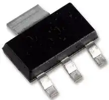
- No. of Pins: 4Pins
- Product Range: -
- Qualification: -
- Power Dissipation: 1.5W
- Transistor Mounting: Surface Mount
- Transistor Polarity: NPN
- Transition Frequency: -
- Transistor Case Style: SOT-223
- DC Current Gain hFE Min: 25hFE
- Operating Temperature Max: 150°C
- Continuous Collector Current: 1.5A
- Collector Emitter Voltage Max: 45V
| Delivery and price | |
|---|---|
| Units per pack | 2000 |
| Price | 0.174 € |
| Current stock | 1000+ |
| Lead time | 7 days |
## **Is Now Part of** ## **To learn more about ON Semiconductor, please visit our website at www.onsemi.com** Please note: As part of the Fairchild Semiconductor integration, some of the Fairchild orderable part numbers will need to change in order to meet ON Semiconductor’s system requirements. Since the ON Semiconductor product management systems do not have the ability to manage part nomenclature that utilizes an underscore (_), the underscore (_) in the Fairchild part numbers will be changed to a dash (-). This document may contain device numbers with an underscore (_). Please check the ON Semiconductor website to verify the updated device numbers. The most current and up-to-date ordering information can be found at www.onsemi.com. Please email any questions regarding the system integration to Fairchild_questions@onsemi.com. ON Semiconductor and the ON Semiconductor logo are trademarks of Semiconductor Components Industries, LLC dba ON Semiconductor or its subsidiaries in the United States and/or other countries. ON Semiconductor owns the rights to a number of patents, trademarks, copyrights, trade secrets, and other intellectual property. A listing of ON Semiconductor’s product/patent coverage may be accessed at www.onsemi.com/site/pdf/Patent-Marking.pdf. ON Semiconductor reserves the right to make changes without further notice to any products herein. ON Semiconductor makes no warranty, representation or guarantee regarding the suitability of its products for any particular purpose, nor does ON Semiconductor assume any liability arising out of the application or use of any product or circuit, and specifically disclaims any and all liability, including without limitation special, consequential or incidental damages. Buyer is responsible for its products and applications using ON Semiconductor products, including compliance with all laws, regulations and safety requirements or standards, regardless of any support or applications information provided by ON Semiconductor. “Typical” parameters which may be provided in ON Semiconductor data sheets and/or specifications can and do vary in different applications and actual performance may vary over time. All operating parameters, including “Typicals” must be validated for each customer application by customer’s technical experts. ON Semiconductor does not convey any license under its patent rights nor the rights of others. ON Semiconductor products are not designed, intended, or authorized for use as a critical component in life support systems or any FDA Class 3 medical devices or medical devices with a same or similar classification in a foreign jurisdiction or any devices intended for implantation in the human body. Should Buyer purchase or use ON Semiconductor products for any such unintended or unauthorized application, Buyer shall indemnify and hold ON Semiconductor and its officers, employees, subsidiaries, affiliates, and distributors harmless against all claims, costs, damages, and expenses, and reasonable attorney fees arising out of, directly or indirectly, any claim of personal injury or death associated with such unintended or unauthorized use, even if such claim alleges that ON Semiconductor was negligent regarding the design or manufacture of the part. ON Semiconductor is an Equal Opportunity/Affirmative Action Employer. This literature is subject to all applicable copyright laws and is not for resale in any manner. ## **BCP54** **==> picture [94 x 68] intentionally omitted <==** **----- Start of picture text -----**<br> C<br>E<br>C<br>B<br>SOT-223<br>**----- End of picture text -----**<br> ## **NPN General Purpose Amplifier** This device is designed for general purpose medium power amplifiers and switching circuits requiring collector currents to 1.2 A. Sourced from Process 38. **Absolute Maximum Ratings*** TA = 25°C unless otherwise noted |**Absolute Maximum Ratings*gs*s***TA = 25°C unless otherwise noted|| |---|---| |**Symbol**<br>**Parameter**|**Value**| |Collector-Emitter Voltage|45| |Collector-Base Voltage|45| |Emitter-Base Voltage|5.0| |Collector Current - Continuous|1.5| |Operating and Storage Junction Temperature Range|-55 to +150| *These ratings are limiting values above which the serviceability of any semiconductor device may be impaired. ## **NOTES** : **1)** These ratings are based on a maximum junction temperature of 150 degrees C. **2)** These are steady state limits. The factory should be consulted on applications involving pulsed or low duty cycle operations. ## **Thermal Characteristics** ## TA = 25°C unless otherwise noted |**Symbol**<br>**Characteristic**|**Max**| |---|---| ||**BCP54**| |Total Device Dissipation<br>Derate above 25°C|1.5<br>12| |Thermal Resistance, Junction to Ambient|83.3| 1997 Fairchild Semiconductor Corporation ## **NPN General Purpose Amplifier** (continued) ## **Electrical Characteristics** TA = 25°C unless otherwise noted |**Electri**|**cal Characteristics**TA|= 25°C unless otherwise noted|||| |---|---|---|---|---|---| |**Symbol**|**Parameter**|**Test Conditions**|**Min**|**Max**|**Units**| |OFF CHARACTERISTICS|||||| |V(BR)CEO|Collector-Emitter Breakdown Voltag|e<br>IC= 10 mA, IB= 0|45||V| |V(BR)CBO|Collector-Base Breakdown Voltage|IC= 100µA, IE= 0|45||V| |V(BR)EBO|Emitter-Base Breakdown Voltage|IE= 10µA, IC= 0|5.0||V| |ICBO|Collector-Cutoff Current|VCB= 30 V, IE= 0<br>VCB= 30 V,IE= 0,TA= 125°C||100<br>10|nA<br>µA| |IEBO|Emitter-Cutoff Current|VEB= 5.0 V, IC= 0||10|µA| |ON CHARACTERISTICS|||||| |hFE|DC Current Gain|IC= 5.0 mA, VCE= 2.0 V<br>IC= 150 mA, VCE= 2.0 V<br>IC= 500 mA,VCE= 2.0 V|25<br>40<br>25|250|| |VCE(sat)|Collector-Emitter Saturation Voltage|IC= 500 mA, IB= 50 mA||0.5|V| |VBE(on)|Base-Emitter On Voltage|IC= 500 mA, VCE= 2.0 V||1.0|V| ## **Typical Characteristics** **==> picture [405 x 153] intentionally omitted <==** **----- Start of picture text -----**<br> Typical Pulsed Current Gain Collector-Emitter Saturation<br>vs Collector Current Voltage vs Collector Current<br>500 0.6<br>β = 10<br>400 V = 5VCE 0.5<br>125 °C 0.4 125 °C<br>300<br>25 °C 0.3 25°C<br>200<br>0.2<br>- 40 °C<br>100 0.1 - 40 °C<br>0 0<br>0.001 0.01 0.1 1 2 0.01 0.1 1 3<br>I - COLLECTOR CURRENT (A)C I - COLLECTOR CURRENT (A)C<br>FE CESAT<br>h - TYPICAL PULSED CURRENT GAIN<br>V - COLLECTOR-EMITTER VOLTAGE (V)<br>**----- End of picture text -----**<br> **==> picture [450 x 667] intentionally omitted <==** **----- Start of picture text -----**<br> NPN General Purpose Amplifier<br>(continued)<br>Typical Characteristics (continued)<br>Base-Emitter Saturation Base-Emitter ON Voltage vs<br>Voltage vs Collector Current Collector Current<br>1<br>1.2 β = 10<br>1 0.8 - 40 °C<br>- 40 °C 25°C<br>0.8<br>0.6<br>25°C 125 °C<br>0.6<br>125 °C<br>0.4 0.4 V = 5VCE<br>0.2 0.2<br>1 10 100 1000 0.001 0.01 0.1 1<br>I - COLLECTOR CURRENT (mA)C I - COLLECTOR CURRENT (A)C<br>Collector-Cutoff Current Collector-Base Capacitance<br>vs Ambient Temperature vs Collector-Base Voltage<br>100 40<br>V = 40VCB<br>10 30<br>1 20<br>0.1 10<br>0<br>25 50 75 100 125 150 0 4 8 12 16 20 24 28<br>T - AMBIENT TEMPERATURE ( C)A ° V - COLLECTOR-BASE VOLTAGE (V)CB<br>Gain Bandwidth Product Power Dissipation vs<br>vs Collector Current Ambient Temperature<br>500 1.5<br>V = 10VCE<br>1.25<br>400<br>SOT-223<br>1<br>300<br>0.75<br>200<br>0.5<br>100<br>0.25<br>0 1 10 100 1000 0 0 25 50 75 100 125 150<br>I - COLLECTOR CURRENT (mA)C TEMPERATURE ( C)o<br>BE(ON)<br>BESAT<br>OBO<br>D<br>FE<br>V - BASE-EMITTER VOLTAGE (V)<br>V - BASE-EMITTER ON VOLTAGE (V)<br>I - COLLECTOR CURRENT (nA)CBO<br> - COLLECTOR-BASE CAPACITANCE (pF)<br>P - POWER DISSIPATION (W)<br>h - GAIN BANDWIDTH PRODUCT (MHz)<br>**----- End of picture text -----**<br> ## **SOT-223 Tape and Reel Data** **==> picture [441 x 579] intentionally omitted <==** **----- Start of picture text -----**<br> SOT-223 Packaging<br>Configuration: Figure 1.0<br>Customized Label<br>Packaging Description:<br>SOT-223 parts are shipped in tape. The carrier tape is<br>made from a dissipative (carbon filled) polycarbonate<br>F63TNR Label resin. The cover tape is a multilayer film (Heat Activated<br>Adhesive in nature) primarily composed of polyester film,<br>Antistatic Cover T ape adhesive layer, sealant, and anti-static sprayed agent.These reeled parts in standard option are shipped with<br>2,500 units per 13" or 330cm diameter reel. The reels are<br>dark blue in color and is made of polystyrene plastic (anti-<br>static coated). Other option comes in 500 units per 7" or<br>177cm diameter reel. This and some other options are<br>further described in the Packaging Information table.<br>These full reels are individually barcode labeled and<br>placed inside a standard intermediate box (illustrated in<br>figure 1.0) made of recyclable corrugated brown paper.<br>One box contains two reels maximum. And these boxes<br>are placed inside a barcode labeled shipping box which<br>Static Dissipative comes in different sizes depending on the number of parts<br> Embossed Carrier Tape shipped.<br>F852 F852 F852 F852<br>014 014 014 014<br>SOT-223 Packaging Information<br>Packaging OptionPackaging type (no flow code)StandardTNR D84ZTNR SOT-223 Unit Orientation<br>Qty per Reel/Tube/Bag 2,500 500<br>Reel Size 13" Dia 7" Dia<br>Box Dimension (mm) 343x64x343 184x187x47<br>Max qty per Box 5,000 1,000 343mm x 342mm x 64mm<br>Weight per unit (gm) 0.1246 0.1246<br>Weight per Reel (kg) 0.7250 0.1532 Intermediate box for Standard F63TNR Label<br>Note/Comments<br>F63TNR Label<br>F63TNR Label sample<br>184mm x 184mm x 47mm<br>Pizza Box for D84Z Option LOT: CBVK741B019 QTY: 3000<br>FSID: PN2222A SPEC:<br>SOT-223 Tape Leader and Trailer<br>D/C1: D9842 QTY1: SPEC REV:<br>Configuration: Figure 2.0 D/C2: QTY2: CPN:<br>N/F: F (F63TNR)3<br>Carrier Tape<br>Cover Tape Trailer Tape Components Leader Tape<br>300mm minimum or 500mm minimum or<br>38 empty pockets 62 empty pockets<br>**----- End of picture text -----**<br> September 1999, Rev. B ©2000 Fairchild Semiconductor International ## **SOT-223 Tape and Reel Data, continued** **==> picture [413 x 592] intentionally omitted <==** **----- Start of picture text -----**<br> SOT-223 Embossed Carrier Tape<br>Configuration: Figure 3.0 P0 D0<br>T<br>E1<br>F<br>K0 E2 W<br>Wc B0<br>Tc<br>A0 P1 D1<br>User Direction of Feed<br>Dimensions are in millimeter<br>Pkg type A0 B0 W D0 D1 E1 E2 F P1 P0 K0 T Wc Tc<br>SOT-223 (12mm) 6.83+/-0.10 7.42+/-0.10 12.0+/-0.3 1.55+/-0.05 1.50+/-0.10 1.75+/-0.10 10.25min 5.50+/-0.05 8.0+/-0.1 4.0+/-0.1 1.88+/-0.10 0.292+/-0.0130 9.5+/-0.025 0.06+/-0.02<br>Notes: A0, B0, and K0 dimensions are determined with respect to the EIA/Jedec RS-481<br>rotational and lateral movement requirements (see sketches A, B, and C). 0.5mm<br>20 deg maximum maximum<br>Typical<br>component<br>cavity 0.5mm<br>B0 center line maximum<br>20 deg maximum component rotation<br>Typical<br>Sketch A (Side or Front Sectional View) Component Rotation A0 componentcenter line Sketch C (Top View) Component lateral movement<br>Sketch B (Top View)<br>SOT-223 Reel Configuration: Figure 4.0 Component Rotation<br>W1 Measured at Hub<br>Dim A<br>Max<br>Dim A See detail AA<br>max Dim N<br>7" Diameter Option<br>B Min<br>Dim C<br>See detail AA Dim D<br>W3 min<br>13" Diameter Option W2 max Measured at Hub<br>DETAIL AA<br>Dimensions are in inches and millimeters<br>Reel<br>Tape Size Dim A Dim B Dim C Dim D Dim N Dim W1 Dim W2 Dim W3 (LSL-USL)<br>Option<br>12mm 7" Dia 7.00177.8 0.0591.5 512 +0.020/-0.00813 +0.5/-0.2 0.79520.2 5.906150 0.488 +0.078/-0.00012.4 +2/0 0.72418.4 0.469 – 0.60611.9 – 15.4<br>12mm 13" Dia 13.00330 0.0591.5 512 +0.020/-0.00813 +0.5/-0.2 0.79520.2 7.00178 0.488 +0.078/-0.00012.4 +2/0 0.72418.4 0.469 – 0.60611.9 – 15.4<br>**----- End of picture text -----**<br> July 1999, Rev. B ## **SOT-223 Package Dimensions** **==> picture [231 x 18] intentionally omitted <==** **----- Start of picture text -----**<br> SOT-223 (FS PKG Code 47)<br>**----- End of picture text -----**<br> **==> picture [148 x 71] intentionally omitted <==** **----- Start of picture text -----**<br> 1 : 1<br>Scale 1:1 on letter size paper<br>Part Weight per unit (gram): 0.1246<br>**----- End of picture text -----**<br> September 1999, Rev. C ©2000 Fairchild Semiconductor International ## **TRADEMARKS** The following are registered and unregistered trademarks Fairchild Semiconductor owns or is authorized to use and is not intended to be an exhaustive list of all such trademarks. |ACEx™|FASTr™|PowerTrench<br>||SyncFET™| |---|---|---|---|---| |Bottomless™|GlobalOptoisolator™|QFET™||TinyLogic™| |CoolFET™|GTO™|QS™||UHC™| |_CROSSVOLT_™|HiSeC™|QT Optoelectronics™||VCX™| |DOME™|ISOPLANAR™|Quiet Series™||| |E2CMOSTM|MICROWIRE™|SILENT SWITCHER||| |EnSignaTM|OPTOLOGIC™|SMART START™||| |FACT™|OPTOPLANAR™|SuperSOT™-3||| |FACT Quiet Series™|PACMAN™|SuperSOT™-6||| |<br>FAST|POP™|SuperSOT™-8||| ## **DISCLAIMER** FAIRCHILD SEMICONDUCTOR RESERVES THE RIGHT TO MAKE CHANGES WITHOUT FURTHER NOTICE TO ANY PRODUCTS HEREIN TO IMPROVE RELIABILITY, FUNCTION OR DESIGN. FAIRCHILD DOES NOT ASSUME ANY LIABILITY ARISING OUT OF THE APPLICATION OR USE OF ANY PRODUCT OR CIRCUIT DESCRIBED HEREIN; NEITHER DOES IT CONVEY ANY LICENSE UNDER ITS PATENT RIGHTS, NOR THE RIGHTS OF OTHERS. ## **LIFE SUPPORT POLICY** FAIRCHILD’S PRODUCTS ARE NOT AUTHORIZED FOR USE AS CRITICAL COMPONENTS IN LIFE SUPPORT DEVICES OR SYSTEMS WITHOUT THE EXPRESS WRITTEN APPROVAL OF FAIRCHILD SEMICONDUCTOR CORPORATION. As used herein: 1. Life support devices or systems are devices or 2. A critical component is any component of a life systems which, (a) are intended for surgical implant into support device or system whose failure to perform can the body, or (b) support or sustain life, or (c) whose be reasonably expected to cause the failure of the life failure to perform when properly used in accordance support device or system, or to affect its safety or with instructions for use provided in the labeling, can be effectiveness. reasonably expected to result in significant injury to the user. ## **PRODUCT STATUS DEFINITIONS** ## **Definition of Terms** |**Datasheet Identification**|**Product Status**|**Definition**| |---|---|---| |Advance Information|Formative or<br>In Design|This datasheet contains the design specifications for<br>product development. Specifications may change in<br>any manner without notice.| |Preliminary|First Production|This datasheet contains preliminary data, and<br>supplementary data will be published at a later date.<br>Fairchild Semiconductor reserves the right to make<br>changes at any time without notice in order to improve<br>design.| |No Identification Needed|Full Production|This datasheet contains final specifications. Fairchild<br>Semiconductor reserves the right to make changes at<br>any time without notice in order to improve design.| |Obsolete|Not In Production|This datasheet contains specifications on a product<br>that has been discontinued by Fairchild semiconductor.<br>The datasheet is printed for reference information only.| Rev. G ON Semiconductor and are trademarks of Semiconductor Components Industries, LLC dba ON Semiconductor or its subsidiaries in the United States and/or other countries. ON Semiconductor owns the rights to a number of patents, trademarks, copyrights, trade secrets, and other intellectual property. A listing of ON Semiconductor’s product/patent coverage may be accessed at www.onsemi.com/site/pdf/Patent−Marking.pdf. ON Semiconductor reserves the right to make changes without further notice to any products herein. ON Semiconductor makes no warranty, representation or guarantee regarding the suitability of its products for any particular purpose, nor does ON Semiconductor assume any liability arising out of the application or use of any product or circuit, and specifically disclaims any and all liability, including without limitation special, consequential or incidental damages. Buyer is responsible for its products and applications using ON Semiconductor products, including compliance with all laws, regulations and safety requirements or standards, regardless of any support or applications information provided by ON Semiconductor. “Typical” parameters which may be provided in ON Semiconductor data sheets and/or specifications can and do vary in different applications and actual performance may vary over time. All operating parameters, including “Typicals” must be validated for each customer application by customer’s technical experts. ON Semiconductor does not convey any license under its patent rights nor the rights of others. ON Semiconductor products are not designed, intended, or authorized for use as a critical component in life support systems or any FDA Class 3 medical devices or medical devices with a same or similar classification in a foreign jurisdiction or any devices intended for implantation in the human body. Should Buyer purchase or use ON Semiconductor products for any such unintended or unauthorized application, Buyer shall indemnify and hold ON Semiconductor and its officers, employees, subsidiaries, affiliates, and distributors harmless against all claims, costs, damages, and expenses, and reasonable attorney fees arising out of, directly or indirectly, any claim of personal injury or death associated with such unintended or unauthorized use, even if such claim alleges that ON Semiconductor was negligent regarding the design or manufacture of the part. ON Semiconductor is an Equal Opportunity/Affirmative Action Employer. This literature is subject to all applicable copyright laws and is not for resale in any manner. ## **PUBLICATION ORDERING INFORMATION** **N. American Technical Support** : 800−282−9855 Toll Free **ON Semiconductor Website** : **www.onsemi.com** USA/Canada ## **LITERATURE FULFILLMENT** : Literature Distribution Center for ON Semiconductor **Order Literature** : http://www.onsemi.com/orderlit For additional information, please contact your local Sales Representative 19521 E. 32nd Pkwy, Aurora, Colorado 80011 USA **Europe, Middle East and Africa Technical Support: Phone** : 303−675−2175 or 800−344−3860 Toll Free USA/Canada Phone: 421 33 790 2910 **Fax** : 303−675−2176 or 800−344−3867 Toll Free USA/Canada **Japan Customer Focus Center Email** : orderlit@onsemi.com Phone: 81−3−5817−1050 © Semiconductor Components Industries, LLC www.onsemi.com **www.onsemi.com** **1**
Updated at March 24, 2026
onsemi is a premier global supplier of intelligent power and sensing technologies, driving disruptive innovations across the automotive, industrial, and cloud infrastructure markets. Recognized for their commitment to sustainability and reliable supply chains, the company accelerates advancements in vehicle electrification, industrial automation, and 5G networks by solving the industry's most complex design challenges. At the core of their portfolio is an industry-leading selection of discrete semiconductors. This extensive range features thousands of high-performance bipolar transistors, single and dual MOSFETs, and a comprehensive array of diodes, including Zener, Schottky, and fast-recovery rectifiers. Engineered for superior thermal performance and energy efficiency, these foundational components are critical for demanding power conversion, switching, and signal conditioning applications. Beyond essential discretes, onsemi provides a robust suite of advanced power management and circuit protection solutions. Their lineup includes intelligent power modules, single IGBTs, and transient voltage suppression (TVS) diodes designed to safeguard sensitive circuitry. Complimented by integrated passive filters, AC/DC LED driver ICs, and specialized sub-2.4GHz RF transceivers, onsemi equips engineers with the scalable, high-quality technologies needed to build a cleaner, smarter, and more connected world.
About Novapart
Novapart is a B2B electronic component broker specialising in stock shortages and cost reduction. We source hard-to-find parts and identify compliant alternatives across a catalogue of 410,000+ components from 500+ manufacturers.
Learn more →Stock Shortage Specialist
When a component is unavailable, discontinued or has an unacceptable lead time, we tap into our network of vetted European and Asian distributors to source what you need — without compromising on quality or traceability.
Request a quote →Compliant Alternatives
We identify pin-to-pin, electrically equivalent substitutes that meet the same certifications (RoHS, AEC-Q100, REACH) as your original specification — validated against datasheets, not just part numbers. Often at a lower cost.
BOM Analysis service →