


BC847BE6327HTSA1
Bipolar (BJT) Single Transistor, NPN, 45 V, 100 mA, 330 mW, SOT-23, Surface Mount
- Manufacturer: INFINEON
- Product type: Single Bipolar Junction Transistors - BJT
- Transistor Polarity:NPN; Collector Emitter Voltage V(br)ceo:45V; Transition Frequency ft:250MHz; Power Dissipation Pd:330mW; DC Collector Current:100mA; DC Current Gain hFE:200hFE;
- MSL: MSL 1 - Unlimited
- SVHC: No SVHC (25-Jun-2025)
- No. of Pins: 3Pins
- Product Range: -
- Qualification: AEC-Q101
- Power Dissipation: 330mW
- Transistor Mounting: Surface Mount
- Transistor Polarity: NPN
- Transition Frequency: 250MHz
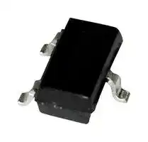
- Transistor Case Style: SOT-23
- DC Current Gain hFE Min: 200hFE
- Operating Temperature Max: 150°C
- Continuous Collector Current: 100mA
- Collector Emitter Voltage Max: 45V
| Delivery and price | |
|---|---|
| Units per pack | 24000 |
| Price | 0.032 € |
| Current stock | 1000+ |
| Lead time | 7 days |
**BC846...-BC850...**

## **NPN Silicon AF Transistors**

- For AF input stages and driver applications

- High current gain

- Low collector-emitter saturation voltage

- Low noise between 30 Hz and 15 kHz

- Complementary types:

BC856...-BC860...(PNP)

- Pb-free (RoHS compliant) package[1)]

- Qualified according AEC Q101

- 1Pb-containing package may be available upon special request

2008-04-29

1

**BC846...-BC850...**

|**Type**|**Marking**|**Pin Configuration**|**Pin Configuration**|**Pin Configuration**|**Pin Configuration**|**Pin Configuration**|**Pin Configuration**|**Package**|
|---|---|---|---|---|---|---|---|---|
|BC846A<br>BC846B<br>BC846BW<br>BC847A<br>BC847B<br>BC847BF*<br>BC847BL3<br>BC847BW<br>BC847C<br>BC847CW<br>BC848A<br>BC848B<br>BC848BL3<br>BC848BW<br>BC848CW<br>BC849B<br>BC849C<br>BC849CW<br>BC850B<br>BC850BW<br>BC850C<br>BC850CW|1As<br>1Bs<br>1Bs<br>1Es<br>1Fs<br>1Fs<br>1F<br>1Fs<br>1Gs<br>1Gs<br>1Js<br>1Ks<br>1K<br>1Ks<br>1Ls<br>2Bs<br>2Cs<br>2Cs<br>2Fs<br>2Fs<br>2Gs<br>2Gs|1=B<br>1=B<br>1=B<br>1=B<br>1=B<br>1=B<br>1=B<br>1=B<br>1=B<br>1=B<br>1=B<br>1=B<br>1=B<br>1=B<br>1=B<br>1=B<br>1=B<br>1=B<br>1=B<br>1=B<br>1=B<br>1=B|2=E<br>2=E<br>2=E<br>2=E<br>2=E<br>2=E<br>2=E<br>2=E<br>2=E<br>2=E<br>2=E<br>2=E<br>2=E<br>2=E<br>2=E<br>2=E<br>2=E<br>2=E<br>2=E<br>2=E<br>2=E<br>2=E|3=C<br>3=C<br>3=C<br>3=C<br>3=C<br>3=C<br>3=C<br>3=C<br>3=C<br>3=C<br>3=C<br>3=C<br>3=C<br>3=C<br>3=C<br>3=C<br>3=C<br>3=C<br>3=C<br>3=C<br>3=C<br>3=C|-<br>-<br>-<br>-<br>-<br>-<br>-<br>-<br>-<br>-<br>-<br>-<br>-<br>-<br>-<br>-<br>-<br>-<br>-<br>-<br>-<br>-|-<br>-<br>-<br>-<br>-<br>-<br>-<br>-<br>-<br>-<br>-<br>-<br>-<br>-<br>-<br>-<br>-<br>-<br>-<br>-<br>-<br>-|-<br>-<br>-<br>-<br>-<br>-<br>-<br>-<br>-<br>-<br>-<br>-<br>-<br>-<br>-<br>-<br>-<br>-<br>-<br>-<br>-<br>-|SOT23<br>SOT23<br>SOT323<br>SOT23<br>SOT23<br>TSFP-3<br>TSLP-3-1<br>SOT323<br>SOT23<br>SOT323<br>SOT23<br>SOT23<br>TSLP-3-1<br>SOT323<br>SOT323<br>SOT23<br>SOT23<br>SOT323<br>SOT23<br>SOT323<br>SOT23<br>SOT323|


* Not for new design

2008-04-29

2

**BC846...-BC850...**

|**Maximum Ratings**|**Maximum Ratings**|**Maximum Ratings**|**Maximum Ratings**|
|---|---|---|---|
|**Parameter**|**Symbol**|**Value**|**Unit**|
|Collector-emitter voltage<br>BC846...<br>BC847..., BC850...<br>BC848..., BC849...|_V_CEO|65<br>45<br>30|V|
|Collector-emitter voltage<br>BC846...<br>BC847..., BC850...<br>BC848..., BC849...|_V_CES|80<br>50<br>30||
|Collector-base voltage<br>BC846...<br>BC847..., BC850...<br>BC848..., BC849...|_V_CBO|80<br>50<br>30||
|Emitter-base voltage<br>BC846...<br>BC847..., BC850...<br>BC848..., BC849...|_V_EBO|6<br>6<br>6||
|Collector current|_I_C|100|mA|
|Peak collector current, _t_p ≤10 ms|_I_CM|200||
|Total power dissipation-<br>_T_S≤71 °C, BC846-BC850<br>_T_S≤128 °C, BC847F<br>_T_S≤135 °C, BC847L3-BC848L3<br>_T_S≤124 °C, BC846W-BC850W|_P_tot|330<br>250<br>250<br>250|mW|
|Junction temperature|_T_j|150|°C|
|Storage temperature|_T_stg|-65 ... 150||
|**Thermal Resistance**||||
|**Parameter**|**Symbol**|**Value**|**Unit**|
|Junction - soldering point1)<br>BC846-BC850<br>BC847F<br>BC847L3-BC848L3<br>BC846W-BC850W|_R_thJS|≤240<br>≤90<br>≤60<br>≤105|K/W|


> 1For calculation of _R_ thJA please refer to Application Note Thermal Resistance

2008-04-29

3

**BC846...-BC850...**

|**Electrical Characteristics**at_T_A= 25°C, unless otherwise specified|**Electrical Characteristics**at_T_A= 25°C, unless otherwise specified|**Electrical Characteristics**at_T_A= 25°C, unless otherwise specified|**Electrical Characteristics**at_T_A= 25°C, unless otherwise specified|**Electrical Characteristics**at_T_A= 25°C, unless otherwise specified|**Electrical Characteristics**at_T_A= 25°C, unless otherwise specified|
|---|---|---|---|---|---|
|**Parameter**|**Symbol**|**Values**|||**Unit**|
|||**min.**|**typ.**|**max.**||
|**DC Characteristics**||||||
|Collector-emitter breakdown voltage<br>_I_C= 10 mA,_I_B= 0 , BC846...<br>_I_C= 10 mA,_I_B= 0 , BC847..., BC850...<br>_I_C= 10 mA,_I_B= 0 , BC848..., BC849...|_V_(BR)CEO|65<br>45<br>30|-<br>-<br>-|-<br>-<br>-|V|
|Collector-base breakdown voltage<br>_I_C= 10 µA,_I_E= 0 , BC846...<br>_I_C= 10 µA,_I_E= 0 , BC847..., BC850...<br>_I_C= 10 µA,_I_E= 0 , BC848..., BC849...|_V_(BR)CBO|80<br>50<br>30|-<br>-<br>-|-<br>-<br>-||
|Emitter-base breakdown voltage<br>_I_E= 0 ,_I_C= 10 µA|_V_(BR)EBO|-|6|-||
|Collector-base cutoff current<br>_V_CB= 45 V,_I_E= 0<br>_V_CB= 30 V,_I_E= 0 ,_T_A= 150 °C|_I_CBO|-<br>-|0.015<br>5|-<br>-|µA|
|DC current gain1)<br>_I_C= 10 µA,_V_CE= 5 V,_h_FE-grp.A<br>_I_C= 10 µA,_V_CE= 5 V,_h_FE-grp.B<br>_I_C= 10 µA,_V_CE= 5 V,_h_FE-grp.C<br>_I_C= 2 mA,_V_CE= 5 V,_h_FE-grp.A<br>_I_C= 2 mA,_V_CE= 5 V,_h_FE-grp.B<br>_I_C= 2 mA,_V_CE= 5 V,_h_FE-grp.C|_h_FE|-<br>-<br>-<br>110<br>200<br>420|140<br>250<br>480<br>180<br>290<br>520|-<br>-<br>-<br>220<br>450<br>800|-|
|Collector-emitter saturation voltage1)<br>_I_C= 10 mA,_I_B= 0.5 mA<br>_I_C= 100 mA,_I_B= 5 mA|_V_CEsat|-<br>-|90<br>200|250<br>600|mV|
|Base emitter saturation voltage1)<br>_I_C= 10 mA,_I_B= 0.5 mA<br>_I_C= 100 mA,_I_B= 5 mA|_V_BEsat|-<br>-|700<br>900|-<br>-||
|Base-emitter voltage1)<br>_I_C= 2 mA,_V_CE= 5 V<br>_I_C= 10 mA,_V_CE= 5 V|_V_BE(ON)|580<br>-|660<br>-|700<br>770||


1Pulse test: t < 300µs; D < 2%

2008-04-29

4

**BC846...-BC850...**

## **Electrical Characteristics** at _T_ A = 25°C, unless otherwise specified

|**Electrical Characteristics**at_T_A= 25°C,unless o|therwise s|pecified|pecified|pecified||
|---|---|---|---|---|---|
|**Parameter**|**Symbol**|**Values**|||**Unit**|
|||**min.**|**typ.**|**max.**||
|**AC Characteristics**||||||
|Transition frequency<br>_I_C= 10 mA,_V_CE= 5 V,_f_= 100 MHz|_f_T|-|250|-|MHz|
|Collector-base capacitance<br>_V_CB= 10 V,_f_= 1 MHz|_C_cb|-|0.95|-|pF|
|Emitter-base capacitance<br>_V_EB= 0.5 V,_f_= 1 MHz|_C_eb|-|9|-||
|Short-circuit input impedance<br>_I_C= 2 mA,_V_CE= 5 V,_f_= 1 kHz,_h_FE-grp.A<br>_I_C= 2 mA,_V_CE= 5 V,_f_= 1 kHz,_h_FE-grp.B<br>_I_C= 2 mA,_V_CE= 5 V,_f_= 1 kHz,_h_FE-grp.C|_h_11e|-<br>-<br>-|2.7<br>4.5<br>8.7|-<br>-<br>-|kΩ|
|Open-circuit reverse voltage transf. ratio<br>_I_C= 2 mA,_V_CE= 5 V,_f_= 1 kHz,_h_FE-grp.A<br>_I_C= 2 mA,_V_CE= 5 V,_f_= 1 kHz,_h_FE-grp.B<br>_I_C= 2 mA,_V_CE= 5 V,_f_= 1 kHz,_h_FE-grp.C|_h_12e|-<br>-<br>-|1.5<br>2<br>3|-<br>-<br>-|10-4|
|Short-circuit forward current transf. ratio<br>_I_C= 2 mA,_V_CE= 5 V,_f_= 1 kHz,_h_FE-grp.A<br>_I_C= 2 mA,_V_CE= 5 V,_f_= 1 kHz,_h_FE-grp.B<br>_I_C= 2 mA,_V_CE= 5 V,_f_= 1 kHz,_h_FE-grp.C|_h_21e|-<br>-<br>-|200<br>330<br>600|-<br>-<br>-||
|Open-circuit output admittance<br>_I_C= 2 mA,_V_CE= 5 V,_f_= 1 kHz,_h_FE-grp.A<br>_I_C= 2 mA,_V_CE= 5 V,_f_= 1 kHz,_h_FE-grp.B<br>_I_C= 2 mA,_V_CE= 5 V,_f_= 1 kHz,_h_FE-grp.C|_h_22e|-<br>-<br>-|18<br>30<br>60|-<br>-<br>-|µS|
|Noise figure<br>_I_C= 200 µA,_V_CE= 5 V,_f_= 1 kHz,<br>∆ _f_= 200Hz,_R_S= 2kΩ, BC849..., BC850...|_F_|-|1.2|4|dB|
|Equivalent noise voltage<br>_I_C= 200 µA,_V_CE= 5 V,_R_S= 2kΩ,<br>_f_= 10 ... 50 Hz , BC850...|_V_n|-|-|0.135|µV|


2008-04-29

5

**BC846...-BC850...**

**DC current gain** _h_ FE =  ƒ( _I_ C) _V_ CE = 5 V

**==> picture [234 x 268] intentionally omitted <==**

**----- Start of picture text -----**<br>
10 3 EHP00365<br>h FE 5 100 C<br>25 C<br>-50 C<br>10 [2]<br>5<br>10 [1]<br>5<br>10 0<br>10 -2 5 10 -1 5 10 0 5 10 1 mA 10 2<br>Ι<br> C<br>**----- End of picture text -----**<br>


## **Base-emitter saturation voltage**

_I_ C =  ƒ( _V_ BEsat), _h_ FE = 20

**==> picture [236 x 265] intentionally omitted <==**

**----- Start of picture text -----**<br>
10 2 EHP00364<br>Ι C mA<br>100 C<br>25 C<br>-50 C<br>10 [1]<br>5<br>10 [0]<br>5<br>10 -1<br>0 0.2 0.4 0.6 0.8 V 1.2<br>V BEsat<br>**----- End of picture text -----**<br>


**Collector-emitter saturation voltage** _I_ C = ƒ( _V_ CEsat), _h_ FE = 20

**==> picture [232 x 267] intentionally omitted <==**

**----- Start of picture text -----**<br>
10 2 EHP00367<br>mA<br>Ι<br>C<br>100 C<br>25 C<br>-50 C<br>10 1<br>5<br>0<br>10<br>5<br>10 -1<br>0 0.1 0.2 0.3 0.4 V 0.5<br>V<br>CEsat<br>**----- End of picture text -----**<br>


**Collector cutoff current** _I_ CBO =  ƒ( _T_ A) _V_ CB = 30 V

**==> picture [232 x 264] intentionally omitted <==**

**----- Start of picture text -----**<br>
10 4 EHP00415<br>nA<br>ΙCB0<br>max<br>10 3<br>5<br>typ<br>10 2<br>5<br>1<br>10<br>5<br>10 0<br>0 50 100 ˚C 150<br>T A<br>**----- End of picture text -----**<br>


2008-04-29

6

**BC846...-BC850...**

**Transition frequency** _f_ T =  ƒ( _I_ C) _V_ CE = 5 V

**Collector-base capacitance** _C_ cb = ƒ( _V_ CB) **Emitter-base capacitance** _C_ eb = ƒ( _V_ EB)

**==> picture [233 x 267] intentionally omitted <==**

**----- Start of picture text -----**<br>
10 3 EHP00363<br>MHz<br>f T 5<br>10 [2]<br>5<br>10 1<br>10 -1 5 10 0 5 10 1 mA 10 2<br>Ι C<br>**----- End of picture text -----**<br>


**Total power dissipation** _P_ tot = ƒ( _T_ S) BC846-BC850

**==> picture [238 x 267] intentionally omitted <==**

**----- Start of picture text -----**<br>
13<br>pF<br>11<br>10<br>9<br>8<br>7<br>6<br>CEB<br>5<br>4<br>3<br>2<br>1<br>CCB<br>0<br>0 4 8 12 16 V 22<br>V CB/ V EB<br>EB<br>C<br>CB/<br>C<br>**----- End of picture text -----**<br>


**Total power dissipation** _P_ tot = ƒ( _T_ S) BC847BF

**==> picture [485 x 267] intentionally omitted <==**

**----- Start of picture text -----**<br>
360  300<br>mW mW<br>300  250<br>270  225<br>240  200<br>210  175<br>180  150<br>150  125<br>120  100<br>90  75<br>60  50<br>30  25<br>0 0<br>0 15 30 45 60 75 90 105 120 °C 150 0 15 30 45 60 75 90 105 120 °C 150<br>T S T S<br>tot tot<br>P P<br>**----- End of picture text -----**<br>


2008-04-29

7

**BC846...-BC850...**

## **Total power dissipation** _P_ tot = ƒ( _T_ S) BC847BL3/BC848BL3

**Total power dissipation** _P_ tot = ƒ( _T_ S) BC846W-BC850W

**==> picture [485 x 267] intentionally omitted <==**

**----- Start of picture text -----**<br>
300  300<br>mW mW<br>250  250<br>225  225<br>200  200<br>175  175<br>150  150<br>125  125<br>100  100<br>75  75<br>50  50<br>25  25<br>0 0<br>0 15 30 45 60 75 90 105 120 °C 150 0 15 30 45 60 75 90 105 120 °C 150<br>T S T S<br>tot tot<br>P P<br>**----- End of picture text -----**<br>


## **Permissible Pulse Load**

_P_ totmax/ _P_ totDC =  ƒ( _t_ p) BC846/W-BC850/W

**==> picture [230 x 266] intentionally omitted <==**

**----- Start of picture text -----**<br>
10 3 EHP00362<br>P totmax t<br>t  p<br>P tot DC D = p<br>T<br>T<br>10 [2] D =<br>0<br>0.005<br>5<br>0.01<br>0.02<br>0.05<br>0.1<br>0.2<br>0.5<br>10 [1]<br>5<br>10 0<br>-6<br>10 10 [-5] 10 [-4] 10 [-3] 10 [-2] s 10 [0]<br>t<br>p<br>**----- End of picture text -----**<br>


**Permissible Puls Load** _R_ thJS = ƒ ( _t_ p) BC847BF

**==> picture [235 x 272] intentionally omitted <==**

**----- Start of picture text -----**<br>
10 2<br>K/W<br>10 1  D=0.5<br>0.2<br>0.1<br>0.05<br>0.02<br>0.01<br>0.005<br>0<br>10 0<br>10 -1<br>10  [-6 ] 10  [-5 ] 10  [-4 ] 10  [-3 ] 10  [-2 ] s 10  [0 ]<br>t<br>p<br>thJS<br>R<br>**----- End of picture text -----**<br>


2008-04-29

8

**BC846...-BC850...**

## **Permissible Pulse Load**

_P_ totmax/ _P_ totDC =  ƒ( _t_ p) BC847BF

**==> picture [234 x 272] intentionally omitted <==**

**----- Start of picture text -----**<br>
10 3<br>10 2  D=0<br>0.005<br>0.01<br>0.02<br>0.05<br>0.1<br>0.2<br>10 1  0.5<br>10 0<br>10  [-6 ] 10  [-5 ] 10  [-4 ] 10  [-3 ] 10  [-2 ] s 10  [0 ]<br>t<br>p<br>totDC<br>/ P totmax<br>P<br>**----- End of picture text -----**<br>


## **Permissible Pulse Load**

_P_ totmax/ _P_ totDC =  ƒ( _t_ p) BC847BL3, BC848BL3

**==> picture [233 x 272] intentionally omitted <==**

**----- Start of picture text -----**<br>
10 3<br>D = 0<br>10 2  0.005<br>0.01<br>0.02<br>0.05<br>0.1<br>0.2<br>0.5<br>10 1<br>10 0<br>10  [-7 ] 10  [-6 ] 10  [-5 ] 10  [-4 ] 10  [-3 ] 10  [-2 ] s 10  [0 ]<br>t<br>p<br>totDC<br>P<br>/<br>totmax<br>P<br>**----- End of picture text -----**<br>


**Permissible Puls Load** _R_ thJS = ƒ ( _t_ p) BC847BL3, BC848BL3

**==> picture [233 x 272] intentionally omitted <==**

**----- Start of picture text -----**<br>
10 2<br>10 1<br>0.5<br>0.2<br>0.1<br>0.05<br>10 0  0.02<br>0.01<br>0.005<br>D = 0<br>10 -1<br>10  [-7 ] 10  [-6 ] 10  [-5 ] 10  [-4 ] 10  [-3 ] 10  [-2 ] s 10  [0 ]<br>t<br>p<br>thJS<br>R<br>**----- End of picture text -----**<br>


**Noise figure** _F_ =  ƒ( _V_ CE) _I_ C = 0.2mA, _R_ S = 2kΩ , _f_ = 1kHz

**==> picture [233 x 266] intentionally omitted <==**

**----- Start of picture text -----**<br>
BC 846...850 EHP00370<br>20<br>dB<br>F<br>15<br>10<br>5<br>0<br>10 -1 5 10 0 10 1 V 10 2<br>V<br>CE<br>**----- End of picture text -----**<br>


2008-04-29

9

**BC846...-BC850...**

**Noise figure** _F_ =  ƒ( _f_ ) _I_ C = 0.2 mA, _V_ CE = 5V, _R_ S = 2 kΩ

**==> picture [230 x 263] intentionally omitted <==**

**----- Start of picture text -----**<br>
BC 846...850 EHP00371<br>20<br>dB<br>F<br>15<br>10<br>5<br>0<br>10 -2 10 -1 10 0 10 1 kHz 10 2<br>f<br>**----- End of picture text -----**<br>


**Noise figure** _F_ =  ƒ( _I_ C) _V_ CE = 5V, _f_ = 1kHz

**==> picture [228 x 263] intentionally omitted <==**

**----- Start of picture text -----**<br>
BC 846...850 EHP00373<br>20<br>dB<br>F<br>15<br>R S = 1 MΩ 100 kΩ 10 kΩ<br>10<br>1 k Ω<br>5<br>500 Ω<br>0<br>10 -3 10 -2 10 -1 10 0 mA 10 1<br>ΙC<br>**----- End of picture text -----**<br>


**Noise figure** _F_ =  ƒ( _I_ C) _V_ CE = 5V, _f_ = 120Hz

**==> picture [227 x 264] intentionally omitted <==**

**----- Start of picture text -----**<br>
BC 846...850 EHP00372<br>20<br>dB<br>F<br>15<br>R S = 1 MΩ 100 kΩ 10 kΩ<br>10<br>500 Ω<br>5<br>1 k Ω<br>0<br>10 -3 10 -2 10 -1 10 0 mA 10 1<br>ΙC<br>**----- End of picture text -----**<br>


**Noise figure** _F_ =  ƒ( _I_ C) _V_ CE = 5V, _f_ = 10kHz

**==> picture [231 x 265] intentionally omitted <==**

**----- Start of picture text -----**<br>
BC 846...850 EHP00374<br>20<br>dB<br>F<br>15<br>R S = 1 MΩ<br>100 kΩ<br>10<br>500 Ω 10 kΩ<br>5<br>1 kΩ<br>0<br>10 -3 10 -2 10 -1 10 0 mA 101<br>ΙC<br>**----- End of picture text -----**<br>


2008-04-29

10

**Package SOT23**

**BC846...-BC850...**

## Package Outline

**==> picture [244 x 457] intentionally omitted <==**

**----- Start of picture text -----**<br>
1±0.1<br>2.9 ±0.1 0.1 MAX.<br>B<br>3<br>1 2<br>+0.1 1)<br>0.4 -0.05 A<br>C<br>0.95<br>1.9<br>0.25 M B C 0.2 M A<br>1) Lead width can be 0.6 max. in dambar area<br>0.8<br>0.8 1.2<br>Manufacturer<br>2005, June<br>EH s Date code (YM)<br>Pin 1 BCW66<br>Type code<br>0...8˚<br>0.08...0.15<br>0.15 MIN.<br> ±0.15 ±0.1<br>2.4 1.3<br>10˚ MAX. 10˚ MAX.<br>0.9<br>1.3<br>0.9<br>**----- End of picture text -----**<br>


## Foot Print

## Marking Layout (Example)

## Standard Packing

Reel ø180 mm = 3.000 Pieces/Reel Reel ø330 mm = 10.000 Pieces/Reel

**==> picture [174 x 91] intentionally omitted <==**

**----- Start of picture text -----**<br>
4<br>0.9 0.2<br>Pin 1 3.15 1.15<br>2.13 2.65<br>8<br>**----- End of picture text -----**<br>


2008-04-29

11

**Package SOT323**

**BC846...-BC850...**

## Package Outline

**==> picture [199 x 124] intentionally omitted <==**

**----- Start of picture text -----**<br>
2 ±0.2 0.9 ±0.1<br>0.1 MAX.<br>0.3 [+0.1] -0.05 3x<br>0.1 M 0.1<br>A<br>3<br>1 2<br>0.65 0.65 0.15 [+0.1] -0.05<br>0.2 M A<br>±0.1  ±0.1<br>2.1 0.1 MIN. 1.25<br>**----- End of picture text -----**<br>


## Foot Print

**==> picture [75 x 95] intentionally omitted <==**

**----- Start of picture text -----**<br>
0.6<br>0.65<br>0.65<br>1.6<br>0.8<br>**----- End of picture text -----**<br>


## Marking Layout (Example)

**==> picture [152 x 96] intentionally omitted <==**

**----- Start of picture text -----**<br>
Manufacturer<br>2005, June<br>Date code (YM)<br>Pin 1 BCR108W<br>Type code<br>**----- End of picture text -----**<br>


## Standard Packing

Reel ø180 mm = 3.000 Pieces/Reel Reel ø330 mm = 10.000 Pieces/Reel

**==> picture [155 x 80] intentionally omitted <==**

**----- Start of picture text -----**<br>
4 0.2<br>Pin 1 2.15 1.1<br>8<br>2.3<br>**----- End of picture text -----**<br>


2008-04-29

12

**Package TSFP-3**

**BC846...-BC850...**

**==> picture [494 x 693] intentionally omitted <==**

**----- Start of picture text -----**<br>
Package Outline<br>1.2 ±0.05<br>0.2 ±0.05 0.55 ±0.04<br>3<br>1 2<br>0.2 ±0.05 0.15 ±0.05<br>0.4 [±0.05]<br>0.4 [±0.05]<br>Foot Print<br>0.4<br>0.4 0.4<br>Marking Layout (Example)<br>Manufacturer<br>BCR847BF<br>Pin 1<br>Type code<br>Standard Packing<br>Reel ø180 mm = 3.000 Pieces/Reel<br>Reel ø330 mm = 10.000 Pieces/Reel<br>4<br>0.3 0.2<br>Pin 1 1.35 0.7<br>±0.05<br>0.8<br>±0.05 ±0.05<br>10˚ MAX.<br>1.2 0.2<br>0.45<br>1.05<br>1.2 1.5<br>8<br>**----- End of picture text -----**<br>


2008-04-29

13

**Package TSLP-3-1**

**BC846...-BC850...**

## Package Outline

**==> picture [295 x 454] intentionally omitted <==**

**----- Start of picture text -----**<br>
Top view Bottom view<br>0.4 [+0.1] 0.6 ±0.05<br>0.05 MAX. 0.5 ±0.0351)<br>3<br>3<br>1 2<br>2 1<br>0.35 ±0.05<br>Pin 1<br>marking 2x0.15 ±0.0351)<br>1) Dimension applies to plated terminal<br>For board assembly information please refer to Infineon website "Packages"<br>0.6<br>0.45<br>0.2 R0.1<br>0.225<br>0.2<br>0.225<br>0.17<br>0.15<br>Copper Solder mask Stencil apertures<br>BFR193L3<br>Type code<br>Pin 1 marking<br>Laser marking<br>1)<br>±0.035<br>0.25<br>±0.05<br>±0.05<br>1<br>0.65<br>1)<br>±0.035<br>0.25<br>2x<br>0.275<br>0.35 0.355<br>1 0.3<br>0.945<br>0.35<br>0.315<br>**----- End of picture text -----**<br>


## Foot Print

For board assembly information please refer to Infineon website "Packages"

Marking Layout (Example)

## Standard Packing

Reel ø180 mm = 15.000 Pieces/Reel

**==> picture [152 x 85] intentionally omitted <==**

**----- Start of picture text -----**<br>
4 0.5<br>Pin 1 0.76<br>marking<br>1.16 8<br>**----- End of picture text -----**<br>


2008-04-29

14

**BC846...-BC850...**

Edition 2006-02-01 Published by Infineon Technologies AG 81726 München, Germany © Infineon Technologies AG 2007. All Rights Reserved.

## **Attention please!**

The information given in this dokument shall in no event be regarded as a guarantee of conditions or characteristics (“Beschaffenheitsgarantie”). With respect to any examples or hints given herein, any typical values stated herein and/or any information regarding the application of the device, Infineon Technologies hereby disclaims any and all warranties and liabilities of any kind, including without limitation warranties of non-infringement of intellectual property rights of any third party.

## **Information**

For further information on technology, delivery terms and conditions and prices please contact your nearest Infineon Technologies Office ( **www.infineon.com** ).

## **Warnings**

Due to technical requirements components may contain dangerous substances. For information on the types in question please contact your nearest Infineon Technologies Office.

Infineon Technologies Components may only be used in life-support devices or systems with the express written approval of Infineon Technologies, if a failure of such components can reasonably be expected to cause the failure of that life-support device or system, or to affect the safety or effectiveness of that device or system.

Life support devices or systems are intended to be implanted in the human body, or to support and/or maintain and sustain and/or protect human life. If they fail, it is reasonable to assume that the health of the user or other persons may be endangered.

2008-04-29

15
Updated at March 24, 2026
Infineon Technologies is a globally recognized leader in semiconductor solutions, renowned for driving innovation in power management, energy efficiency, and modern mobility. With a strong legacy of engineering excellence, the company provides highly reliable components designed to meet the rigorous demands of industrial, automotive, and advanced commercial applications. The core of our Infineon portfolio is centered on their industry-leading discrete semiconductors. We offer an extensive selection of single and dual MOSFETs, alongside a robust range of single IGBTs and advanced IGBT modules. These flagship power transistors are essential for high-efficiency power conversion and motor control, providing engineers with superior thermal performance and minimized switching losses. Beyond advanced field-effect transistors, the selection includes a comprehensive array of diodes and rectifiers, heavily featuring Schottky diodes, as well as fast-recovery and RF/PIN diodes. This power foundation is further supported by bipolar transistors, intelligent power modules, and thyristor SCR modules, delivering the critical building blocks required for complex power system designs. To support broader system integration, the portfolio also encompasses specialized solutions such as solid-state relays, AC/DC LED driver ICs, and Bluetooth communications modules. From high-power industrial rectifiers to wireless connectivity adapters, Infineon equips designers with the precision components needed to build efficient, scalable, and fully connected electronic systems.
About Novapart
Novapart is a B2B electronic component broker specialising in stock shortages and cost reduction. We source hard-to-find parts and identify compliant alternatives across a catalogue of 410,000+ components from 500+ manufacturers.
Learn more →Stock Shortage Specialist
When a component is unavailable, discontinued or has an unacceptable lead time, we tap into our network of vetted European and Asian distributors to source what you need — without compromising on quality or traceability.
Request a quote →Compliant Alternatives
We identify pin-to-pin, electrically equivalent substitutes that meet the same certifications (RoHS, AEC-Q100, REACH) as your original specification — validated against datasheets, not just part numbers. Often at a lower cost.
BOM Analysis service →