


BAS716,115
Small Signal Diode, Single, 85 V, 200 mA, 1.25 V, 3 µs, 4 A
- Manufacturer: NEXPERIA
- Product type: Small Signal Diodes
- Diode Configuration:Single; Repetitive Reverse Voltage Vrrm Max:85V; Forward Current If(AV):200mA; Forward Voltage VF Max:1.25V; Reverse Recovery Time trr Max:3µs; Forward Surge Current Ifsm Ma
- SVHC: No SVHC (25-Jun-2025)
- No. of Pins: 2Pins
- Product Range: -
- Qualification: -
- Diode Mounting: Surface Mount
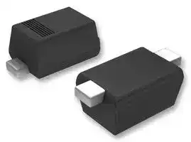
- Diode Case Style: SOD-523
- Diode Configuration: Single
- Forward Voltage Max: 1.25V
- Forward Surge Current: 4A
- Reverse Recovery Time: 3µs
- Average Forward Current: 200mA
- Operating Temperature Max: 150°C
- Repetitive Peak Reverse Voltage: 85V
| Delivery and price | |
|---|---|
| Units per pack | 1500 |
| Price | 0.077 € |
| Current stock | 10+ |
| Lead time | 30 days |
## _**DISCRETE SEMICONDUCTORS**_

**==> picture [359 x 51] intentionally omitted <==**

**----- Start of picture text -----**<br>
DATA SHEET<br>**----- End of picture text -----**<br>


**==> picture [207 x 206] intentionally omitted <==**

**----- Start of picture text -----**<br>
M3D319<br>**----- End of picture text -----**<br>


**BAS716** Low-leakage diode

Product data sheet

**==> picture [249 x 119] intentionally omitted <==**

2003 Nov 07

**NXP Semiconductors**

**Product data sheet**

**BAS716**

## **Low-leakage diode**

## **FEATURES**

- Plastic SMD package

- Low leakage current: typ. 0.2 nA

- Switching time: typ. 0.6 µs

- Continuous reverse voltage: max. 75 V

- Repetitive peak reverse voltage: max. 85 V

- Repetitive peak forward current: max. 500 mA.

## **APPLICATION**

- Low leakage current applications in surface mounted circuits.

## **DESCRIPTION**

Epitaxial medium-speed switching diode with a low leakage current in an ultra small SOD523 (SC-79) SMD plastic package.

## **PINNING**

|**PINNING**|**PINNING**|**PINNING**|**PINNING**|**PINNING**|||
|---|---|---|---|---|---|---|
|**PIN**|||||**DESCRIPTION**||
|1|||||cathode||
|2|||||anode||
||||||||
||||||||
|_handbook, halfpage_**1**<br>||||**2**|||
||||||||
|Top view<br>_MAM408_|||||||
|Fig.1<br>Simplified outline (SOD523; SC-79) and<br>symbol.<br>**Marking code:**S1.<br>The marking bar indicates the cathode.|||||||


## **ORDERING INFORMATION**

|**TYPE NUMBER**|**PACKAGE**|**PACKAGE**|**PACKAGE**|
|---|---|---|---|
||**NAME**|**DESCRIPTION**|**VERSION**|
|BAS716|−|plastic surface mountedpackage; 2 leads|SOD523|


## **LIMITING VALUES**

In accordance with the Absolute Maximum Rating System (IEC 60134).

|**SYMBOL**|**PARAMETER**|**CONDITIONS**|**MIN.**|**MAX.**|**UNIT**|
|---|---|---|---|---|---|
|VRRM|repetitivepeak reverse voltage||−|85|V|
|VR|continuous reverse voltage||−|75|V|
|IF|continuous forward current|see Fig.2; note 1|−|200|mA|
|IFRM|repetitivepeak forward current||−|500|mA|
|IFSM|non-repetitive peak forward current|square wave; Tj= 25°C prior to surge;<br>see Fig.4<br>tp= 1µs<br>tp= 1 ms<br>tp= 1 s|−<br>−<br>−|4<br>1<br>0.5|A<br>A<br>A|
|Ptot|totalpower dissipation|Tamb= 25°C; note 1|−|250|mW|
|Tstg|storage temperature||−65|+150|°C|
|Tj|junction temperature||−|150|°C|


## **Note**

1. Device mounted on a FR4 printed-circuit board.

2003 Nov 07

2

NXP Semiconductors

Product data sheet

## Low-leakage diode

## BAS716

## **ELECTRICAL CHARACTERISTICS**

Tj =  25 °C unless otherwise specified.

|**SYMBOL**|**PARAMETER**|**CONDITIONS**|**TYP.**|**MAX.**|**UNIT**|
|---|---|---|---|---|---|
|VF|forward voltage|IF= 1 mA|0.77|0.9|V|
|||IF= 10 mA|0.85|1|V|
|||IF= 50 mA|0.92|1.1|V|
|||IF= 150 mA|1.02|1 .25|V|
|IR|reverse current|VR= 75 V|0.2|5|nA|
|||VR= 75 V; Tj= 150°C|3|80|nA|
|||VR= 100 V|0.3|−|nA|
|Cd|diode capacitance|VR= 0 V; f = 1 MHz; see Fig.6|2|−|pF|
|trr|reverse recovery time|when switched from IF= 10 mA to<br>IR= 10 mA; RL= 100Ω; measured at<br>IR= 1 mA|0.6|3|µs|


## **THERMAL CHARACTERISTICS**

|**SYMBOL**|**PARAMETER**|**CONDITIONS**|**VALUE**|**UNIT**|
|---|---|---|---|---|
|Rthj-a|thermal resistance fromjunction to ambient|note 1|450|K/W|
|Rthj-s|thermal resistance fromjunction to soldering point|note 2|120|K/W|


## **Notes**

1. Device mounted on a FR4 printed-circuit board. Refer to SOD523 (SC-79) standard mounting conditions.

2. Soldering point of the cathode tab.

2003 Nov 07

3

NXP Semiconductors

Product data sheet

## Low-leakage diode

## BAS716

## **GRAPHICAL DATA**

**==> picture [497 x 608] intentionally omitted <==**

**----- Start of picture text -----**<br>
MHC323 MLB752 - 1<br>300 300<br>handbook, halfpage handbook, halfpage<br>IF IF<br>(mA) (mA)<br>200 200<br>(1) (2) (3)<br>100 100<br>0 0<br>0 100 200 0 0.4 0.8 1.2 1.6<br>Tamb ( ° C) V    (V)F<br>(1) Tj = 150 °C; typical values.<br>Device mounted on a FR4 printed-circuit board.  (2) Tj = 25 °C; typical values.<br>(3) Tj = 25 °C; maximum values.<br>Fig.2 Maximum permissible continuous forward<br>current as a function of ambient  Fig.3 Forward current as a function of forward<br>temperature. voltage.<br>MBG704<br>10 [2]<br>handbook, full pagewidth<br>IFSM<br>(A)<br>10<br>1<br>10 [−] [1]<br>1 10 10 [2] 10 [3] 10 [4]<br>tp ( µ s)<br>Based on square wave currents; Tj = 25 °C prior to surge.<br>Fig.4  Maximum permissible non-repetitive peak forward current as a function of pulse duration.<br>**----- End of picture text -----**<br>


2003 Nov 07

4

NXP Semiconductors

Product data sheet

## Low-leakage diode

## BAS716

**==> picture [242 x 306] intentionally omitted <==**

**----- Start of picture text -----**<br>
MDB826<br>10 [2]<br>handbook, halfpage<br>IR<br>(nA) (1)<br>10<br>(2)<br>1<br>10 [−] [1]<br>0 50 100 150 Tj ( ° C) 200<br>VR = 75 V.<br>(1) Maximum values.<br>(2) Typical values.<br>Fig.5 Reverse current as a function of junction<br>temperature.<br>**----- End of picture text -----**<br>


**==> picture [242 x 306] intentionally omitted <==**

**----- Start of picture text -----**<br>
MDB827<br>2.0<br>handbook, halfpage<br>Cd<br>(pF)<br>1.5<br>1.0<br>0.5<br>0<br>0 5 10 15 20<br>VR (V)<br>f = 1 MHz; Tj = 25 °C.<br>Fig.6 Diode capacitance as a function of reverse<br>voltage; typical values.<br>**----- End of picture text -----**<br>


**==> picture [497 x 305] intentionally omitted <==**

**----- Start of picture text -----**<br>
handbook, full pagewidth<br>tr t p<br>t<br>D.U.T. 10%<br>R   = 50SS Ω IF SAMPLING IF t rr t<br>OSCILLOSCOPE<br>V = V      I   x RRR F S R  = 50ii Ω<br>90% (1)<br>VR<br>MGA881<br>input signal output signal<br>(1) IR = 1 mA.R = 1 mA. = 1 mA.<br>Input signal: reverse pulse rise time tr = 0.6 ns; reverse voltage pulse duration tp = 100 ns; duty factor δ = 0.05;r = 0.6 ns; reverse voltage pulse duration tp = 100 ns; duty factor δ = 0.05; = 0.6 ns; reverse voltage pulse duration tp = 100 ns; duty factor δ = 0.05;p = 100 ns; duty factor δ = 0.05; = 100 ns; duty factor δ = 0.05;δ = 0.05; = 0.05;<br>Oscilloscope: rise time tr = 0.35 ns.r = 0.35 ns. = 0.35 ns.<br>Fig.7  Reverse recovery voltage test circuit and waveforms.<br>**----- End of picture text -----**<br>


2003 Nov 07

5

NXP Semiconductors

Product data sheet

BAS716

## Low-leakage diode

## **PACKAGE OUTLINE**

**==> picture [495 x 293] intentionally omitted <==**

**----- Start of picture text -----**<br>
Plastic surface mounted package; 2 leads SOD523<br>A<br>c<br>HE v M A<br>D A<br>0 0.5 1 mm<br>scale<br>1 2<br>DIMENSIONS (mm are the original dimensions)<br>E bp<br>UNIT A bp c D E HE v<br>0.65 0.34 0.17 1.25 0.85 1.65<br>mm 0.1<br>(1) 0.58 0.26 0.11 1.15 0.75 1.55<br>Note<br>1. The marking bar indicates the cathode.<br>OUTLINE  REFERENCES EUROPEAN<br>ISSUE DATE<br>VERSION  IEC  JEDEC  JEITA PROJECTION<br>98-11-25<br> SOD523 SC-79<br>02-12-13<br>**----- End of picture text -----**<br>


2003 Nov 07

6

NXP Semiconductors

Product data sheet

## Low-leakage diode

## BAS716

## **DATA SHEET STATUS**

|**DATA SHEET STATUS**|||
|---|---|---|
|**DOCUMENT**<br>**STATUS**(1)|**PRODUCT**<br>**STATUS**(2)|**DEFINITION**|
|Objective data sheet|Development|This document contains data from the objective specification for product<br>development.|
|Preliminarydata sheet|Qualification|This document contains data from thepreliminaryspecification.|
|Product data sheet|Production|This document contains theproduct specification.|


## **Notes**

1. Please consult the most recently issued document before initiating or completing a design.

2. The product status of device(s) described in this document may have changed since this document was published and may differ in case of multiple devices. The latest product status information is available on the Internet at URL http://www.nxp.com.

## **DISCLAIMERS**

**General** ⎯ Information in this document is believed to be accurate and reliable. However, NXP Semiconductors does not give any representations or warranties, expressed or implied, as to the accuracy or completeness of such information and shall have no liability for the consequences of use of such information.

**Right to make changes** ⎯ NXP Semiconductors reserves the right to make changes to information published in this document, including without limitation specifications and product descriptions, at any time and without notice. This document supersedes and replaces all information supplied prior to the publication hereof.

**Suitability for use** ⎯ NXP Semiconductors products are not designed, authorized or warranted to be suitable for use in medical, military, aircraft, space or life support equipment, nor in applications where failure or malfunction of an NXP Semiconductors product can reasonably be expected to result in personal injury, death or severe property or environmental damage. NXP Semiconductors accepts no liability for inclusion and/or use of NXP Semiconductors products in such equipment or applications and therefore such inclusion and/or use is at the customer’s own risk.

⎯ **Applications** Applications that are described herein for any of these products are for illustrative purposes only. NXP Semiconductors makes no representation or warranty that such applications will be suitable for the specified use without further testing or modification.

⎯ **Limiting values** Stress above one or more limiting values (as defined in the Absolute Maximum Ratings System of IEC 60134) may cause permanent damage to the device. Limiting values are stress ratings only and operation of the device at these or any other conditions above those given in the Characteristics sections of this document is not implied. Exposure to limiting values for extended periods may affect device reliability.

**Terms and conditions of sale** ⎯ NXP Semiconductors products are sold subject to the general terms and conditions of commercial sale, as published at http://www.nxp.com/profile/terms, including those pertaining to warranty, intellectual property rights infringement and limitation of liability, unless explicitly otherwise agreed to in writing by NXP Semiconductors. In case of any inconsistency or conflict between information in this document and such terms and conditions, the latter will prevail.

**No offer to sell or license** ⎯ Nothing in this document may be interpreted or construed as an offer to sell products that is open for acceptance or the grant, conveyance or implication of any license under any copyrights, patents or other industrial or intellectual property rights.

⎯ **Export control** This document as well as the item(s) described herein may be subject to export control regulations. Export might require a prior authorization from national authorities.

**Quick reference data** ⎯ The Quick reference data is an extract of the product data given in the Limiting values and Characteristics sections of this document, and as such is not complete, exhaustive or legally binding.

2003 Nov 07

7

## _**NXP Semiconductors**_

## **Customer notification**

This data sheet was changed to reflect the new company name NXP Semiconductors. No changes were made to the content, except for the legal definitions and disclaimers.

## **Contact information**

For additional information please visit: **http://www.nxp.com** For sales offices addresses send e-mail to: **salesaddresses@nxp.com**

## © NXP B.V. 2009

All rights are reserved. Reproduction in whole or in part is prohibited without the prior written consent of the copyright owner.

The information presented in this document does not form part of any quotation or contract, is believed to be accurate and reliable and may be changed without notice. No liability will be accepted by the publisher for any consequence of its use. Publication thereof does not convey nor imply any license under patent- or other industrial or intellectual property rights.

Printed in The Netherlands

**==> picture [178 x 143] intentionally omitted <==**

Date of release: 2003 Nov 07

R76/01/pp8

Document order number: 9397 750 11999
Updated at April 28, 2026
Nexperia is a dedicated global leader in discretes, logic, and MOSFET devices. Built on over half a century of semiconductor expertise and operating independently since 2017, the company produces consistently reliable components at an exceptional volume of 85 billion units annually. With its own manufacturing facilities, Nexperia delivers industry-leading small packages that combine power and thermal efficiency with best-in-class quality, meeting the rigorous standards of the automotive sector. Our extensive Nexperia portfolio is heavily focused on discrete semiconductors, providing engineers with a robust selection of core building blocks. This includes a comprehensive range of diodes and rectifiers, featuring a vast selection of Zener single diodes and Schottky diodes designed for precise voltage regulation and efficient power routing. Additionally, we offer an expansive array of bipolar transistors and single MOSFETs tailored for reliable switching and amplification in demanding applications. Beyond these primary offerings, the lineup extends into specialized circuit protection and passive components. This includes transient voltage suppressor (TVS) diodes, Zener array diodes, and small signal diodes, alongside dual MOSFETs and fast recovery rectifiers. For comprehensive design needs, the selection also encompasses integrated passive filters, common mode chokes, and precision timers and oscillators, ensuring a complete solution for high-performance electronic systems.
About Novapart
Novapart is a B2B electronic component broker specialising in stock shortages and cost reduction. We source hard-to-find parts and identify compliant alternatives across a catalogue of 410,000+ components from 500+ manufacturers.
Learn more →Stock Shortage Specialist
When a component is unavailable, discontinued or has an unacceptable lead time, we tap into our network of vetted European and Asian distributors to source what you need — without compromising on quality or traceability.
Request a quote →Compliant Alternatives
We identify pin-to-pin, electrically equivalent substitutes that meet the same certifications (RoHS, AEC-Q100, REACH) as your original specification — validated against datasheets, not just part numbers. Often at a lower cost.
BOM Analysis service →