


BAP65-03,115
RF / Pin Diode, Single, 0.35 ohm, 30 V, SOD-323, 2 Pin, 0.375 pF
- Manufacturer: NXP
- Product type: RF / Pin Diodes
- Diode Configuration:Single; Resistance @ If:0.35ohm; Breakdown Voltage Vbr:30V; Diode Case Style:SOD-323; No. of Pins:2 Pin; Total Capacitance Ct:0.375pF; Forward Current If(AV):100mA; Ope
- MSL: MSL 1 - Unlimited
- SVHC: No SVHC (27-Jun-2024)
- No. of Pins: 2 Pin
- Product Range: BAP65
- Diode Mounting: Surface Mount
- Forward Current: 100mA
- Forward Voltage: 1.1V
- Resistance @ If: 0.35ohm
- Reverse Voltage: 30V
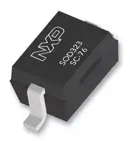
- Diode Case Style: SOD-323
- Diode Capacitance: 0.375pF
- Power Dissipation: 500mW
- Diode Configuration: Single
- Operating Temperature Max: 150°C
| Delivery and price | |
|---|---|
| Units per pack | 5000 |
| Price | 0.105 € |
| Current stock | 1000+ |
| Lead time | 7 days |
## _**DISCRETE SEMICONDUCTORS**_ **==> picture [359 x 51] intentionally omitted <==** **----- Start of picture text -----**<br> DATA SHEET<br>**----- End of picture text -----**<br> **==> picture [206 x 201] intentionally omitted <==** ## **BAP65-03** Silicon PIN diode Product specification Supersedes data of 2001 May 11 2004 Feb 11 **==> picture [203 x 119] intentionally omitted <==** **NXP Semiconductors** **Product specification** ## **Silicon PIN diode** # **BAP65-03** ## **FEATURES** - High voltage, current controlled - RF resistor for RF switches - Low diode capacitance - Low diode forward resistance (low loss) - Very low series inductance. ## **APPLICATIONS** - RF attenuators and switches - Bandswitch for TV tuners - Series diode for mobile communication transmit/receive switch. ## **DESCRIPTION** Planar PIN diode in a SOD323 small SMD plastic package. ## **PINNING** **==> picture [242 x 220] intentionally omitted <==** **----- Start of picture text -----**<br> PIN DESCRIPTION<br>1 cathode<br>2 anode<br>1 2<br>sym006<br>Marking code: D3.<br>The marking bar indicates the cathode.<br>Fig.1 Simplified outline (SOD323) and symbol.<br>**----- End of picture text -----**<br> ## **ORDERING INFORMATION** |**TYPE**<br>**NUMBER**|**PACKAGE**|**PACKAGE**|**PACKAGE**| |---|---|---|---| ||**NAME**|**DESCRIPTION**|**VERSION**| |BAP65-03||plastic surface mountedpackage; 2 leads|SOD323| ## **LIMITING VALUES** In accordance with the Absolute Maximum Rating System (IEC 60134). |**SYMBOL**|**PARAMETER**|**CONDITIONS**|**MIN.**|**MAX.**|**UNIT**| |---|---|---|---|---|---| |VR|continuous reverse voltage|||30|V| |IF|continuous forward current|||100|mA| |Ptot|totalpower dissipation|Ts90C||500|mW| |Tstg|storage temperature||65|+150|C| |Tj|junction temperature||65|+150|C| 2004 Feb 11 2 NXP Semiconductors Product specification ## Silicon PIN diode ## BAP65-03 ## **ELECTRICAL CHARACTERISTICS** Tj = 25 C unless otherwise specified. |**SYMBOL**|**PARAMETER**|**CONDITIONS**|**TYP.**|**MAX.**|**UNIT**| |---|---|---|---|---|---| |VF|forward voltage|IF= 50 mA|0.9|1.1|V| |IR|reverse leakage current|VR= 20 V||20|nA| |Cd|diode capacitance|VR= 0 V; f = 1 MHz|0.65||pF| |||VR= 1 V; f = 1 MHz|0.55|0.9|pF| |||VR= 3 V; f = 1 MHz|0.5|0.8|pF| |||VR= 20 V; f = 1 MHz|0.375||pF| |rD|diode forward resistance|IF= 1 mA; f = 100 MHz|1||| |||IF= 5 mA; f = 100 MHz; note 1|0.65|0.95|| |||IF= 10 mA; f = 100 MHz; note 1|0.56|0.9|| |||IF= 100 mA; f = 100 MHz|0.35||| |s212|isolation|VR= 0; f = 900 MHz|10.2||dB| |||VR= 0; f = 1800 MHz|5.8||dB| |||VR= 0; f = 2450 MHz|4.1||dB| |s212|insertion loss|IF= 1 mA; f = 900 MHz|0.1||dB| |||IF= 1 mA; f = 1800 MHz|0.14||dB| |||IF= 1 mA; f = 2450 MHz|0.18||dB| |s212|insertion loss|IF= 5 mA; f = 900 MHz|0.06||dB| |||IF= 5 mA; f = 1800 MHz|0.1||dB| |||IF= 5 mA; f = 2450 MHz|0.14||dB| |s212|insertion loss|IF= 10 mA; f = 900 MHz|0.06||dB| |||IF= 10 mA; f = 1800 MHz|0.1||dB| |||IF= 10 mA; f = 2450 MHz|0.13||dB| |s212|insertion loss|IF= 100 mA; f = 900 MHz|0.05||dB| |||IF= 100 mA; f = 1800 MHz|0.1||dB| |||IF= 100 mA; f = 2450 MHz|0.14||dB| |L|charge carrier life time|when switched from IF= 10 mA to<br>IR= 6 mA; RL= 100;<br>measured at IR= 3 mA|0.17||s| |LS|series inductance|IF= 100 mA; f = 100 MHz|1.5||nH| ## **Note** 1. Guaranteed on AQL basis: inspection level S4, AQL 1.0. ## **THERMAL CHARACTERISTICS** |**SYMBOL**|**PARAMETER**|**VALUE**|**UNIT**| |---|---|---|---| |Rth(j-s)|thermal resistance fromjunction to soldering point|120|K/W| 2004 Feb 11 3 NXP Semiconductors Product specification ## Silicon PIN diode ## BAP65-03 ## **GRAPHICAL DATA** **==> picture [242 x 278] intentionally omitted <==** **----- Start of picture text -----**<br> MLD503<br>10<br>handbook, halfpage<br>rD<br>( Ω )<br>1<br>10 [−] [1]<br>10 [−] [1] 1 10 10 [2]<br>IF (mA)<br>Tj = 25 C; f = 100 MHz.<br>Fig.2 Forward resistance as a function of forward<br>current; typical values.<br>**----- End of picture text -----**<br> **==> picture [242 x 319] intentionally omitted <==** **----- Start of picture text -----**<br> MLD505<br>0<br>handbook, halfpage<br>s21 [[2]]<br>(dB)dB)) (5)<br>− 0.1<br>− 0.2 (1) (2) (3) (4)<br>− 0.3<br>− 0.4<br>− 0.5<br>0 1000 2000 3000<br>f (MHz)<br>(1) IF = 0.5 mA.F = 0.5 mA. = 0.5 mA. (4) IF = 10 mA.F = 10 mA. = 10 mA.<br>(2) IF = 1 mA.F = 1 mA. = 1 mA. (5) IF = 100 mA.F = 100 mA. = 100 mA.<br>(3) IF = 5 mA.F = 5 mA. = 5 mA.<br>Diode inserted in series with a 50 stripline circuit and biased stripline circuit and biased stripline circuit and biased<br>via the analyzer Tee network; Tamb = 25 C.amb = 25 C. = 25 C. C.C.<br>Fig.4 Insertion loss (s21s21s2121 [[2]] ) of the diode as a<br>function of frequency; typical values.<br>**----- End of picture text -----**<br> **==> picture [242 x 319] intentionally omitted <==** **----- Start of picture text -----**<br> MLD505<br>0<br>handbook, halfpage<br>s21 [[2]]<br>(dB)dB)) (5)<br>− 0.1<br>− 0.2 (1) (2) (3) (4)<br>− 0.3<br>− 0.4<br>− 0.5<br>0 1000 2000 3000<br>f (MHz)<br>(1) IF = 0.5 mA.F = 0.5 mA. = 0.5 mA. (4) IF = 10 mA.F = 10 mA. = 10 mA.<br>(2) IF = 1 mA.F = 1 mA. = 1 mA. (5) IF = 100 mA.F = 100 mA. = 100 mA.<br>(3) IF = 5 mA.F = 5 mA. = 5 mA.<br>Diode inserted in series with a 50 stripline circuit and biased stripline circuit and biased stripline circuit and biased<br>via the analyzer Tee network; Tamb = 25 C.amb = 25 C. = 25 C. C.C.<br>Fig.4 Insertion loss (s21s21s2121 [[2]] ) of the diode as a<br>function of frequency; typical values.<br>**----- End of picture text -----**<br> **==> picture [242 x 278] intentionally omitted <==** **----- Start of picture text -----**<br> MLD504<br>1000<br>handbook, halfpage<br>Cd<br>(fF)<br>800<br>600<br>400<br>200<br>0<br>0 4 8 12 16 20<br>VR (V)<br>Tj = 25 C; f = 1 MHz.<br>Fig.3 Diode capacitance as a function of reverse<br>voltage; typical values.<br>**----- End of picture text -----**<br> **==> picture [242 x 319] intentionally omitted <==** **----- Start of picture text -----**<br> MLD506<br>0<br>handbook, halfpage<br>s21 [[2]]<br>(dB)dB))<br>− 10<br>− 20<br>− 30<br>− 40<br>0 1000 2000 3000<br>f (MHz)<br>Diode zero biased and inserted in series with a 50 stripline circuit. stripline circuit. stripline circuit.<br>Tamb = 25 C.amb = 25 C. = 25 C. C.C.<br>Fig.5 Isolation (s21s21s2121 [[2]] ) of the diode as a function of<br>frequency; typical values.<br>**----- End of picture text -----**<br> **==> picture [242 x 319] intentionally omitted <==** **----- Start of picture text -----**<br> MLD506<br>0<br>handbook, halfpage<br>s21 [[2]]<br>(dB)dB))<br>− 10<br>− 20<br>− 30<br>− 40<br>0 1000 2000 3000<br>f (MHz)<br>Diode zero biased and inserted in series with a 50 stripline circuit. stripline circuit. stripline circuit.<br>Tamb = 25 C.amb = 25 C. = 25 C. C.C.<br>Fig.5 Isolation (s21s21s2121 [[2]] ) of the diode as a function of<br>frequency; typical values.<br>**----- End of picture text -----**<br> 2004 Feb 11 4 NXP Semiconductors Product specification ## Silicon PIN diode ## BAP65-03 ## **PACKAGE OUTLINE** **==> picture [485 x 584] intentionally omitted <==** **----- Start of picture text -----**<br> Plastic surface-mounted package; 2 leads SOD323<br>D A E<br>X<br>HD v M A<br>Q<br>1 2<br>bp<br>A<br>A1<br>(1) c<br>Lp<br>detail X<br>0 1 2 mm<br>scale<br>DIMENSIONS (mm are the original dimensions)<br>UNIT A maxA1 bp c D E HD Lp Q v<br>1.1 0.40 0.25 1.8 1.35 2.7 0.45 0.25<br>mm 0.05 0.2<br>0.8 0.25 0.10 1.6 1.15 2.3 0.15 0.15<br>Note<br>1. The marking bar indicates the cathode<br>OUTLINE REFERENCES EUROPEAN<br>ISSUE DATE<br>VERSION IEC JEDEC JEITA PROJECTION<br>03-12-17<br>SOD323 SC-76<br>06-03-16<br>**----- End of picture text -----**<br> 2004 Feb 11 5 NXP Semiconductors Product specification BAP65-03 ## Silicon PIN diode ## **DATA SHEET STATUS** |**DATA SHEET STATUS**||| |---|---|---| |**DOCUMENT**<br>**STATUS**(1)|**PRODUCT**<br>**STATUS**(2)|**DEFINITION**| |Objective data sheet|Development|This document contains data from the objective specification for product<br>development.| |Preliminarydata sheet|Qualification|This document contains data from thepreliminaryspecification.| |Product data sheet|Production|This document contains theproduct specification.| ## **Notes** 1. Please consult the most recently issued document before initiating or completing a design. 2. The product status of device(s) described in this document may have changed since this document was published and may differ in case of multiple devices. The latest product status information is available on the Internet at URL http://www.nxp.com. ## **DEFINITIONS** **Product specification** The information and data provided in a Product data sheet shall define the specification of the product as agreed between NXP Semiconductors and its customer, unless NXP Semiconductors and customer have explicitly agreed otherwise in writing. In no event however, shall an agreement be valid in which the NXP Semiconductors product is deemed to offer functions and qualities beyond those described in the Product data sheet. ## **DISCLAIMERS** **Limited warranty and liability** Information in this document is believed to be accurate and reliable. However, NXP Semiconductors does not give any representations or warranties, expressed or implied, as to the accuracy or completeness of such information and shall have no liability for the consequences of use of such information. In no event shall NXP Semiconductors be liable for any indirect, incidental, punitive, special or consequential damages (including - without limitation - lost profits, lost savings, business interruption, costs related to the removal or replacement of any products or rework charges) whether or not such damages are based on tort (including negligence), warranty, breach of contract or any other legal theory. Notwithstanding any damages that customer might incur for any reason whatsoever, NXP Semiconductors’ aggregate and cumulative liability towards customer for the products described herein shall be limited in accordance with the _Terms and conditions of commercial sale_ of NXP Semiconductors. **Right to make changes** NXP Semiconductors reserves the right to make changes to information published in this document, including without limitation specifications and product descriptions, at any time and without notice. This document supersedes and replaces all information supplied prior to the publication hereof. **Suitability for use** NXP Semiconductors products are not designed, authorized or warranted to be suitable for use in life support, life-critical or safety-critical systems or equipment, nor in applications where failure or malfunction of an NXP Semiconductors product can reasonably be expected to result in personal injury, death or severe property or environmental damage. NXP Semiconductors accepts no liability for inclusion and/or use of NXP Semiconductors products in such equipment or applications and therefore such inclusion and/or use is at the customer’s own risk. **Applications** Applications that are described herein for any of these products are for illustrative purposes only. NXP Semiconductors makes no representation or warranty that such applications will be suitable for the specified use without further testing or modification. Customers are responsible for the design and operation of their applications and products using NXP Semiconductors products, and NXP Semiconductors accepts no liability for any assistance with applications or customer product design. It is customer’s sole responsibility to determine whether the NXP Semiconductors product is suitable and fit for the customer’s applications and products planned, as well as for the planned application and use of customer’s third party customer(s). Customers should provide appropriate design and operating safeguards to minimize the risks associated with their applications and products. 2004 Feb 11 6 NXP Semiconductors Product specification BAP65-03 ## Silicon PIN diode NXP Semiconductors does not accept any liability related to any default, damage, costs or problem which is based on any weakness or default in the customer’s applications or products, or the application or use by customer’s third party customer(s). Customer is responsible for doing all necessary testing for the customer’s applications and products using NXP Semiconductors products in order to avoid a default of the applications and the products or of the application or use by customer’s third party customer(s). NXP does not accept any liability in this respect. **Limiting values** Stress above one or more limiting values (as defined in the Absolute Maximum Ratings System of IEC 60134) will cause permanent damage to the device. Limiting values are stress ratings only and (proper) operation of the device at these or any other conditions above those given in the Recommended operating conditions section (if present) or the Characteristics sections of this document is not warranted. Constant or repeated exposure to limiting values will permanently and irreversibly affect the quality and reliability of the device. **Terms and conditions of commercial sale** NXP Semiconductors products are sold subject to the general terms and conditions of commercial sale, as published at http://www.nxp.com/profile/terms, unless otherwise agreed in a valid written individual agreement. In case an individual agreement is concluded only the terms and conditions of the respective agreement shall apply. NXP Semiconductors hereby expressly objects to applying the customer’s general terms and conditions with regard to the purchase of NXP Semiconductors products by customer. **Export control** This document as well as the item(s) described herein may be subject to export control regulations. Export might require a prior authorization from national authorities. **Quick reference data** The Quick reference data is an extract of the product data given in the Limiting values and Characteristics sections of this document, and as such is not complete, exhaustive or legally binding. **Non-automotive qualified products** Unless this data sheet expressly states that this specific NXP Semiconductors product is automotive qualified, the product is not suitable for automotive use. It is neither qualified nor tested in accordance with automotive testing or application requirements. NXP Semiconductors accepts no liability for inclusion and/or use of non-automotive qualified products in automotive equipment or applications. In the event that customer uses the product for design-in and use in automotive applications to automotive specifications and standards, customer (a) shall use the product without NXP Semiconductors’ warranty of the product for such automotive applications, use and specifications, and (b) whenever customer uses the product for automotive applications beyond NXP Semiconductors’ specifications such use shall be solely at customer’s own risk, and (c) customer fully indemnifies NXP Semiconductors for any liability, damages or failed product claims resulting from customer design and use of the product for automotive applications beyond NXP Semiconductors’ standard warranty and NXP Semiconductors’ product specifications. **No offer to sell or license** Nothing in this document may be interpreted or construed as an offer to sell products that is open for acceptance or the grant, conveyance or implication of any license under any copyrights, patents or other industrial or intellectual property rights. 2004 Feb 11 7 ## _**NXP Semiconductors**_ ## _**provides High Performance Mixed Signal and Standard Product solutions that leverage its leading RF, Analog, Power Management, Interface, Security and Digital Processing expertise**_ ## **Customer notification** This data sheet was changed to reflect the new company name NXP Semiconductors, including new legal definitions and disclaimers. No changes were made to the technical content, except for package outline drawings which were updated to the latest version. ## **Contact information** For additional information please visit: **http://www.nxp.com** For sales offices addresses send e-mail to: **salesaddresses@nxp.com** ## © NXP B.V. 2010 All rights are reserved. Reproduction in whole or in part is prohibited without the prior written consent of the copyright owner. The information presented in this document does not form part of any quotation or contract, is believed to be accurate and reliable and may be changed without notice. No liability will be accepted by the publisher for any consequence of its use. Publication thereof does not convey nor imply any license under patent- or other industrial or intellectual property rights. Printed in The Netherlands 8 Date of release: 2004 Feb 112004 Feb 11 Date of release: 2004 Feb 112004 Feb 11 R77/04/pp8
Updated at March 24, 2026
NXP Semiconductors is a global leader in secure connectivity solutions, driving innovation across the automotive, industrial, IoT, mobile, and communications infrastructure markets. By developing advanced, purpose-built technologies, NXP enables devices to sense, think, connect, and act intelligently, delivering rigorously tested components that make the connected world safer and more efficient. Within the semiconductor space, NXP is highly regarded for its extensive range of high-performance integrated circuits and discrete devices. The brand's portfolio excels in drivers and interfaces, featuring a comprehensive selection of I/O expanders designed to streamline complex system architectures. For demanding high-frequency and wireless applications, NXP provides industry-leading RF FETs and RF/PIN diodes engineered to deliver exceptional signal integrity, efficiency, and reliability. The NXP product lineup further extends to essential discrete components, including versatile bipolar transistors, JFETs, and small signal diodes optimized for precision switching and amplification. Additionally, the portfolio supports advanced automation and smart applications with precision IC sensors, such as MEMS accelerometers, alongside specialized power management solutions like AC/DC LED driver ICs and single MOSFETs for cutting-edge electronics design.
About Novapart
Novapart is a B2B electronic component broker specialising in stock shortages and cost reduction. We source hard-to-find parts and identify compliant alternatives across a catalogue of 410,000+ components from 500+ manufacturers.
Learn more →Stock Shortage Specialist
When a component is unavailable, discontinued or has an unacceptable lead time, we tap into our network of vetted European and Asian distributors to source what you need — without compromising on quality or traceability.
Request a quote →Compliant Alternatives
We identify pin-to-pin, electrically equivalent substitutes that meet the same certifications (RoHS, AEC-Q100, REACH) as your original specification — validated against datasheets, not just part numbers. Often at a lower cost.
BOM Analysis service →