


BAP50-03,115
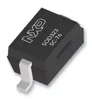
RF / Pin Diode, Single, 5 ohm, 50 V, SOD-323, 2 Pin, 0.35 pF
- Manufacturer: NXP
- Product type: RF / Pin Diodes
- Diode Configuration:Single; Resistance @ If:5ohm; Breakdown Voltage Vbr:50V; Diode Case Style:SOD-323; No. of Pins:2 Pin; Total Capacitance Ct:0.35pF; Forward Current If(AV):50mA; Operating Te
- MSL: MSL 1 - Unlimited
- SVHC: No SVHC (17-Dec-2015)
- No. of Pins: 2 Pin
- Product Range: BAP50
- Diode Mounting: Surface Mount
- Forward Current: 50mA
- Forward Voltage: 1.1V
- Resistance @ If: 5ohm
- Reverse Voltage: 50V
- Diode Case Style: SOD-323
- Diode Capacitance: 0.35pF
- Power Dissipation: 500mW
- Diode Configuration: Single
- Operating Temperature Max: 150°C
| Delivery and price | |
|---|---|
| Units per pack | 25000 |
| Price | 0.036 € |
| Current stock | 10+ |
| Lead time | 30 days |
**==> picture [62 x 50] intentionally omitted <==**

## **BAP50-03**

## **General purpose PIN diode**

**Rev. 04 — 11 September 2009**

## **Product data sheet**

## **1.**

## **1.1 General description**

General purpose PIN diode in a SOD323 small plastic SMD package.

## **1.2 Features**

I Low diode capacitance

I Low diode forward resistance

## **1.3 Applications**

I General RF application

## **2. Pinning information**

|**Table**|**1.**|**Discrete pinning**|||||||||||
|---|---|---|---|---|---|---|---|---|---|---|---|---|
|**Pin**||**Description**|**Simplifed outline**||||||||**Graphic symbol**||
|1||cathode|||||||||||
|2||anode||1|||||2||||
||||||||||||||
||||||||||||sym006||


## **3. Ordering information**

|**formation**|**formation**|**formation**|**formation**|
|---|---|---|---|
|**Table 2.**<br>**Ordering information**||||
|**Type number**|**Package**|||
||**Name**|**Description**|**Version**|
|BAP50-03|SC-76<br>plastic surface-mounted package; 2 leads<br>SOD323|||


**==> picture [211 x 101] intentionally omitted <==**

**BAP50-03**

**NXP Semiconductors**

**General purpose PIN diode**

## **4. Limiting values**

## **Table 3. Limiting values**

In accordance with the Absolute Maximum Rating System (IEC 60134).

|**Symbol**|**Parameter**|**Conditions**|**Min**|**Max**|**Unit**|
|---|---|---|---|---|---|
|**Per diode**||||||
|VR|reverse voltage||-|50|V|
|IF|forward current||-|50|mA|
|Ptot|total power dissipation|Tsp= 90°C|-|500|mW|
|Tstg|storage temperature||−65|+150|°C|
|Tj|junction temperature||−65|+150|°C|


## **5. Thermal characteristics**

## **Table 4. Thermal characteristics**

|**Symbol**|**Parameter**|**Conditions**|**Typ**|**Unit**|
|---|---|---|---|---|
|Rth(j-sp)|thermal resistance from junction||85|K/W|
||to soldering point||||


## **6. Characteristics**

**Table 5. Characteristics** Tj = 25 °C unless otherwise specified.

|**Symbol**<br>**Parameter**|**Conditions**<br>**Min**<br>**Typ**<br>**Max**<br>**Unit**|
|---|---|
|VF<br>forward voltage|IF= 50 mA<br>-<br>0.95<br>1.1<br>V|
|VR<br>reverse voltage|IR= 10µA<br>50<br>-<br>-<br>V|
|IR<br>reverse current|VR= 50 V<br>-<br>-<br>100<br>nA|
|Cd<br>diode capacitance|f = 1 MHz; see<br>Figure<br>1|
||VR= 0 V<br>-<br>0.4<br>-<br>pF|
||VR= 1 V<br>-<br>0.3<br>0.55<br>pF|
||VR= 5 V<br>-<br>0.2<br>0.35<br>pF|
|rD<br>diode forward resistance|f = 100 MHz; see<br>Figure<br>2|
||IF= 0.5 mA<br>[1]<br>-<br>25<br>40<br>Ω|
||IF= 1 mA<br>[1]<br>-<br>14<br>25<br>Ω|
||IF= 10 mA<br>[1]<br>-<br>3<br>5<br>Ω|


[1] Guaranteed on AQL basis: inspection level S4, AQL 1.0.

© NXP B.V. 2009. All rights reserved.

BAP50-03_4

**Rev. 04 — 11 September 2009**

**Product data sheet**

**2 of 7**

**BAP50-03**

**NXP Semiconductors**

## **General purpose PIN diode**

**==> picture [233 x 189] intentionally omitted <==**

**----- Start of picture text -----**<br>
mgs323<br>500<br>Cd<br>(fF)<br>400<br>300<br>200<br>100<br>0<br>0 4 8 12 16 20<br>VR (V)<br>**----- End of picture text -----**<br>


f = 1 MHz; Tj = 25 °C.

**Fig 1. Diode capacitance as a function of reverse voltage; typical values**

**==> picture [233 x 189] intentionally omitted <==**

**----- Start of picture text -----**<br>
mgs319<br>0<br>Lins (1)<br>(dB)<br>−1 (2)<br>(3)<br>−2<br>−3<br>−4<br>−5<br>0.5 1 1.5 2 2.5 3<br>f (GHz)<br>**----- End of picture text -----**<br>


- (1) IF = 10 mA

(2) IF = 1 mA (3) IF = 0.5 mA Tamb = 25 °C. Diode inserted in series with a 50 Ω stripline circuit and biased via the analyzer Tee network.

**Fig 3. Insertion loss of the diode as a function of frequency; typical values**

**==> picture [233 x 189] intentionally omitted <==**

**----- Start of picture text -----**<br>
mgs317<br>10 [3]<br>rD<br>(Ω)<br>10 [2]<br>10<br>1<br>10 [−][2] 10 [−][1] 1 10<br>IF (mA)<br>**----- End of picture text -----**<br>


f = 100 MHz; Tj = 25 °C.

**Fig 2. Diode forward resistance as a function of forward current; typical values**

**==> picture [233 x 189] intentionally omitted <==**

**----- Start of picture text -----**<br>
mgs316<br>0<br>ISL<br>(dB)<br>−5<br>−10<br>−15<br>−20<br>−25<br>0.5 1 1.5 2 2.5 3<br>f (GHz)<br>**----- End of picture text -----**<br>


Tamb = 25 °C. Diode zero biased and inserted in series with a 50 Ω stripline circuit.

**Fig 4. Isolation of the diode as a function of frequency; typical values**

© NXP B.V. 2009. All rights reserved.

BAP50-03_4 **Product data sheet**

**Rev. 04 — 11 September 2009**

**3 of 7**

**BAP50-03**

**NXP Semiconductors**

**General purpose PIN diode**

## **7. Package outline**

## **Plastic surface-mounted package; 2 leads**

## **SOD323**

**==> picture [196 x 126] intentionally omitted <==**

**----- Start of picture text -----**<br>
D A<br>X<br>HD v M A<br>**----- End of picture text -----**<br>


**==> picture [6 x 6] intentionally omitted <==**

**----- Start of picture text -----**<br>
E<br>**----- End of picture text -----**<br>


**==> picture [76 x 58] intentionally omitted <==**

**==> picture [372 x 133] intentionally omitted <==**

**----- Start of picture text -----**<br>
Q<br>1 2<br>bp<br>A<br>A1<br>(1) c<br>Lp<br>detail X<br>**----- End of picture text -----**<br>


|**Note**<br>1. The marking bar indicates the cathode<br>**UNIT**<br>**A**<br>mm<br>0.05<br>1.1<br>0.8<br>0.40<br>0.25<br>0.25<br>0.10<br>1.8<br>1.6<br>1.35<br>1.15<br>2.7<br>2.3<br>0.45<br>0.15<br>**A1**<br>**max**<br>**DIMENSIONS (mm are the original dimensions)**<br>0<br>1<br>2 mm<br>scale<br>**bp**<br>**c**<br>**D**<br>**E**<br>**HD**<br>**Q**<br>0.25<br>0.15<br>**Lp**<br>**v**<br>0.2|**Note**<br>1. The marking bar indicates the cathode<br>**UNIT**<br>**A**<br>mm<br>0.05<br>1.1<br>0.8<br>0.40<br>0.25<br>0.25<br>0.10<br>1.8<br>1.6<br>1.35<br>1.15<br>2.7<br>2.3<br>0.45<br>0.15<br>**A1**<br>**max**<br>**DIMENSIONS (mm are the original dimensions)**<br>0<br>1<br>2 mm<br>scale<br>**bp**<br>**c**<br>**D**<br>**E**<br>**HD**<br>**Q**<br>0.25<br>0.15<br>**Lp**<br>**v**<br>0.2|**Note**<br>1. The marking bar indicates the cathode<br>**UNIT**<br>**A**<br>mm<br>0.05<br>1.1<br>0.8<br>0.40<br>0.25<br>0.25<br>0.10<br>1.8<br>1.6<br>1.35<br>1.15<br>2.7<br>2.3<br>0.45<br>0.15<br>**A1**<br>**max**<br>**DIMENSIONS (mm are the original dimensions)**<br>0<br>1<br>2 mm<br>scale<br>**bp**<br>**c**<br>**D**<br>**E**<br>**HD**<br>**Q**<br>0.25<br>0.15<br>**Lp**<br>**v**<br>0.2|**Note**<br>1. The marking bar indicates the cathode<br>**UNIT**<br>**A**<br>mm<br>0.05<br>1.1<br>0.8<br>0.40<br>0.25<br>0.25<br>0.10<br>1.8<br>1.6<br>1.35<br>1.15<br>2.7<br>2.3<br>0.45<br>0.15<br>**A1**<br>**max**<br>**DIMENSIONS (mm are the original dimensions)**<br>0<br>1<br>2 mm<br>scale<br>**bp**<br>**c**<br>**D**<br>**E**<br>**HD**<br>**Q**<br>0.25<br>0.15<br>**Lp**<br>**v**<br>0.2|**Note**<br>1. The marking bar indicates the cathode<br>**UNIT**<br>**A**<br>mm<br>0.05<br>1.1<br>0.8<br>0.40<br>0.25<br>0.25<br>0.10<br>1.8<br>1.6<br>1.35<br>1.15<br>2.7<br>2.3<br>0.45<br>0.15<br>**A1**<br>**max**<br>**DIMENSIONS (mm are the original dimensions)**<br>0<br>1<br>2 mm<br>scale<br>**bp**<br>**c**<br>**D**<br>**E**<br>**HD**<br>**Q**<br>0.25<br>0.15<br>**Lp**<br>**v**<br>0.2|**Note**<br>1. The marking bar indicates the cathode<br>**UNIT**<br>**A**<br>mm<br>0.05<br>1.1<br>0.8<br>0.40<br>0.25<br>0.25<br>0.10<br>1.8<br>1.6<br>1.35<br>1.15<br>2.7<br>2.3<br>0.45<br>0.15<br>**A1**<br>**max**<br>**DIMENSIONS (mm are the original dimensions)**<br>0<br>1<br>2 mm<br>scale<br>**bp**<br>**c**<br>**D**<br>**E**<br>**HD**<br>**Q**<br>0.25<br>0.15<br>**Lp**<br>**v**<br>0.2|**Note**<br>1. The marking bar indicates the cathode<br>**UNIT**<br>**A**<br>mm<br>0.05<br>1.1<br>0.8<br>0.40<br>0.25<br>0.25<br>0.10<br>1.8<br>1.6<br>1.35<br>1.15<br>2.7<br>2.3<br>0.45<br>0.15<br>**A1**<br>**max**<br>**DIMENSIONS (mm are the original dimensions)**<br>0<br>1<br>2 mm<br>scale<br>**bp**<br>**c**<br>**D**<br>**E**<br>**HD**<br>**Q**<br>0.25<br>0.15<br>**Lp**<br>**v**<br>0.2|**Note**<br>1. The marking bar indicates the cathode<br>**UNIT**<br>**A**<br>mm<br>0.05<br>1.1<br>0.8<br>0.40<br>0.25<br>0.25<br>0.10<br>1.8<br>1.6<br>1.35<br>1.15<br>2.7<br>2.3<br>0.45<br>0.15<br>**A1**<br>**max**<br>**DIMENSIONS (mm are the original dimensions)**<br>0<br>1<br>2 mm<br>scale<br>**bp**<br>**c**<br>**D**<br>**E**<br>**HD**<br>**Q**<br>0.25<br>0.15<br>**Lp**<br>**v**<br>0.2|
|---|---|---|---|---|---|---|---|
|**OUTLINE**<br>**VERSION**|**REFERENCES**||||**EUROPEAN**<br>**PROJECTION**|**ISSUE DATE**||
||**IEC**|**JEDEC**|**JEITA**|||||
|SOD323|||SC-76||||~~03-12-17~~<br>06-03-16|


**Fig 5. Package outline SOD323**

© NXP B.V. 2009. All rights reserved.

BAP50-03_4

**Rev. 04 — 11 September 2009**

**Product data sheet**

**4 of 7**

**BAP50-03**

**NXP Semiconductors**

**General purpose PIN diode**

## **8. Abbreviations**

## **Table 6. Abbreviations**

|**Acronym**|**Description**|
|---|---|
|AQL|Acceptable Quality Level|
|PIN|P-type, Intrinsic, N-type|
|SMD|Surface Mounted Device|
|RF|Radio Frequency|
|S4|Special inspection level 4|


## **9. Revision history**

## **Table 7. Revision history**

|**Document ID**|**Release date**<br>**Data sheet status**|**Change notice**|**Supersedes**|
|---|---|---|---|
|BAP50-03_4|20090911<br>Product data sheet|-|BAP50-03_3|
|Modifcations:|**•** The format of this data sheet has been redesigned to comply with the new identity|||
||guidelines of NXP Semiconductors.|||
||**•** Legal texts have been adapted to the new company name where appropriate.|||
|BAP50-03_3|20040211<br>Product data sheet||BAP50-03_2|
|BAP50-03_2|19990510<br>Product data sheet||BAP50-03_N_1|
|BAP50-03_N_1|19990201<br>Preliminary data sheet||-|


© NXP B.V. 2009. All rights reserved.

BAP50-03_4 **Product data sheet**

**Rev. 04 — 11 September 2009**

**5 of 7**

**BAP50-03**

**NXP Semiconductors**

**General purpose PIN diode**

## **10. Legal information**

## **10.1 Data sheet status**

|**Document statu**|**s**<br>**[1]**<br>**[2]**<br>**Product status**<br>**[3]**<br>**Defnition**|
|---|---|
|Objective [short] data sheet<br>Development<br>This document contains data from the objective specifcation for product development.||
|Preliminary [short] data sheet<br>Qualifcation<br>This document contains data from the preliminary specifcation.||
|Product [short] data sheet<br>Production<br>This document contains the product specifcation.||


[1] Please consult the most recently issued document before initiating or completing a design.

[2]

[3] The product status of device(s) described in this document may have changed since this document was published and may differ in case of multiple devices. The latest product status information is available on the Internet at URL http://www.nxp.com.

## **10.2**

**Draft —** The document is a draft version only. The content is still under internal review and subject to formal approval, which may result in modifications or additions. NXP Semiconductors does not give any representations or warranties as to the accuracy or completeness of information included herein and shall have no liability for the consequences of use of such information.

**Short data sheet —** A short data sheet is an extract from a full data sheet with the same product type number(s) and title. A short data sheet is intended for quick reference only and should not be relied upon to contain detailed and full information. For detailed and full information see the relevant full data sheet, which is available on request via the local NXP Semiconductors sales office. In case of any inconsistency or conflict with the short data sheet, the full data sheet shall prevail.

## **10.3 Disclaimers**

**General —** Information in this document is believed to be accurate and reliable. However, NXP Semiconductors does not give any representations or warranties, expressed or implied, as to the accuracy or completeness of such information and shall have no liability for the consequences of use of such information.

**Right to make changes —** NXP Semiconductors reserves the right to make changes to information published in this document, including without limitation specifications and product descriptions, at any time and without notice. This document supersedes and replaces all information supplied prior to the publication hereof.

**Suitability for use —** NXP Semiconductors products are not designed, authorized or warranted to be suitable for use in medical, military, aircraft, space or life support equipment, nor in applications where failure or malfunction of an NXP Semiconductors product can reasonably be expected to result in personal injury, death or severe property or environmental

damage. NXP Semiconductors accepts no liability for inclusion and/or use of NXP Semiconductors products in such equipment or applications and therefore such inclusion and/or use is at the customer’s own risk.

**Applications —** Applications that are described herein for any of these products are for illustrative purposes only. NXP Semiconductors makes no representation or warranty that such applications will be suitable for the specified use without further testing or modification.

**Limiting values —** the Absolute Maximum Ratings System of IEC 60134) may cause permanent damage to the device. Limiting values are stress ratings only and operation of the device at these or any other conditions above those given in the Characteristics sections of this document is not implied. Exposure to limiting values for extended periods may affect device reliability.

**Terms and conditions of sale —** NXP Semiconductors products are sold subject to the general terms and conditions of commercial sale, as published at http://www.nxp.com/profile/terms, including those pertaining to warranty, intellectual property rights infringement and limitation of liability, unless explicitly otherwise agreed to in writing by NXP Semiconductors. In case of any inconsistency or conflict between information in this document and such terms and conditions, the latter will prevail.

**No offer to sell or license —** Nothing in this document may be interpreted or construed as an offer to sell products that is open for acceptance or the grant, conveyance or implication of any license under any copyrights, patents or other industrial or intellectual property rights.

**Export control —** This document as well as the item(s) described herein may be subject to export control regulations. Export might require a prior authorization from national authorities.

## **10.4 Trademarks**

Notice: All referenced brands, product names, service names and trademarks are the property of their respective owners.

## **11. Contact information**

For more information, please visit: **http://www.nxp.com**

**salesaddresses@nxp.com**

© NXP B.V. 2009. All rights reserved.

BAP50-03_4

**Rev. 04 — 11 September 2009**

**Product data sheet**

**6 of 7**

**BAP50-03**

**NXP Semiconductors**

**General purpose PIN diode**

## **12. Contents**

|**1**|**Product profle . . . . . . . . . . . . . . . . . . . . . . . . . .  1**|
|---|---|
|1.1|General description. . . . . . . . . . . . . . . . . . . . . . 1|
|1.2|Features . . . . . . . . . . . . . . . . . . . . . . . . . . . . . . 1|
|1.3|Applications  . . . . . . . . . . . . . . . . . . . . . . . . . . . 1|
|**2**|**Pinning information. . . . . . . . . . . . . . . . . . . . . .  1**|
|**3**|**Ordering information . . . . . . . . . . . . . . . . . . . . .  1**|
|**4**|**Limiting values. . . . . . . . . . . . . . . . . . . . . . . . . .  2**|
|**5**|**Thermal characteristics. . . . . . . . . . . . . . . . . . .  2**|
|**6**|**Characteristics. . . . . . . . . . . . . . . . . . . . . . . . . .  2**|
|**7**|**Package outline . . . . . . . . . . . . . . . . . . . . . . . . .  4**|
|**8**|**Abbreviations. . . . . . . . . . . . . . . . . . . . . . . . . . .  5**|
|**9**|**Revision history. . . . . . . . . . . . . . . . . . . . . . . . .  5**|
|**10**|**Legal information. . . . . . . . . . . . . . . . . . . . . . . .  6**|
|10.1|Data sheet status . . . . . . . . . . . . . . . . . . . . . . . 6|
|10.2|Defnitions. . . . . . . . . . . . . . . . . . . . . . . . . . . . . 6|
|10.3|Disclaimers . . . . . . . . . . . . . . . . . . . . . . . . . . . . 6|
|10.4|Trademarks. . . . . . . . . . . . . . . . . . . . . . . . . . . . 6|
|**11**|**Contact information. . . . . . . . . . . . . . . . . . . . . .  6**|
|**12**|**Contents . . . . . . . . . . . . . . . . . . . . . . . . . . . . . . .  7**|


**==> picture [151 x 121] intentionally omitted <==**

Please be aware that important notices concerning this document and the product(s) described herein, have been included in section ‘Legal information’.

**© NXP B.V. 2009.**

**All rights reserved.**

For more information, please visit: http://www.nxp.com For sales office addresses, please send an email to: salesaddresses@nxp.com **Date of release: 11 September 2009 Document identifier: BAP50-03_4**
Updated at March 24, 2026
NXP Semiconductors is a global leader in secure connectivity solutions, driving innovation across the automotive, industrial, IoT, mobile, and communications infrastructure markets. By developing advanced, purpose-built technologies, NXP enables devices to sense, think, connect, and act intelligently, delivering rigorously tested components that make the connected world safer and more efficient. Within the semiconductor space, NXP is highly regarded for its extensive range of high-performance integrated circuits and discrete devices. The brand's portfolio excels in drivers and interfaces, featuring a comprehensive selection of I/O expanders designed to streamline complex system architectures. For demanding high-frequency and wireless applications, NXP provides industry-leading RF FETs and RF/PIN diodes engineered to deliver exceptional signal integrity, efficiency, and reliability. The NXP product lineup further extends to essential discrete components, including versatile bipolar transistors, JFETs, and small signal diodes optimized for precision switching and amplification. Additionally, the portfolio supports advanced automation and smart applications with precision IC sensors, such as MEMS accelerometers, alongside specialized power management solutions like AC/DC LED driver ICs and single MOSFETs for cutting-edge electronics design.
About Novapart
Novapart is a B2B electronic component broker specialising in stock shortages and cost reduction. We source hard-to-find parts and identify compliant alternatives across a catalogue of 410,000+ components from 500+ manufacturers.
Learn more →Stock Shortage Specialist
When a component is unavailable, discontinued or has an unacceptable lead time, we tap into our network of vetted European and Asian distributors to source what you need — without compromising on quality or traceability.
Request a quote →Compliant Alternatives
We identify pin-to-pin, electrically equivalent substitutes that meet the same certifications (RoHS, AEC-Q100, REACH) as your original specification — validated against datasheets, not just part numbers. Often at a lower cost.
BOM Analysis service →