
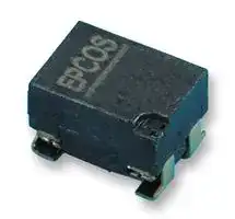


B82799S513N1
INDUCTOR, 51UH, 30%, 100MA,
- Manufacturer: TDK
- Product type: SMD Common Mode Chokes / Filters
- Rated Current:200mA; Inductance:51µH; Product Range:-; Impedance:-; Common Mode Filter Case:4.5mm x 3.2mm x 3mm; Automotive Qualification Standard:-; SVHC:No SVHC (07-Jul-2017); Climatic Cate
- SVHC: No SVHC (15-Jan-2018)
- Impedance: -
- Inductance: 51µH
- Product Range: B82799S0 Series
- Product Width: 3.2mm
- Qualification: -
- Product Height: 3mm
- Product Length: 4.5mm
- DC Current Rating: 200mA
- DC Resistance Max: 0.25ohm
- Operating Temperature Max: 150°C
- Operating Temperature Min: -55°C
| Delivery and price | |
|---|---|
| Units per pack | 25000 |
| Price | 1.53 € |
| Current stock | 10+ |
| Lead time | 30 days |
## **Data and signal line chokes**

Common-mode chokes, ring core, EIA 1812 0.011 … 0.47 mH, 200 … 300 mA, 60 °C

**Series/Type: B82799C0/S0** Date: October 2008

© EPCOS AG 2008. Reproduction, publication and dissemination of this publication, enclosures hereto and the information contained therein without EPCOS’ prior express consent is prohibited.

~~Ce~~ **Data and signal line chokes B82799C0/S0 Common-mode chokes, ring core, EIA 1812**

**Rated voltage 42 V AC/80 V DC Rated inductance 0.011 mH to 0.47 mH Rated current 200 mA to 300 mA**

## **Construction**

- Current-compensated ring core double choke

- Ferrite core

- LCP case (UL 94 V-0)

- Silicone potting

- Bifilar winding (B82799C0)

- Sector winding (B82799S0)

## **Features**

- 150 °C version

- Qualified to AEC-Q200

- Suitable for reflow soldering

- Suitable for conductive adhesion due gold-plated terminals

- RoHS-compatible

## **Function**

## ■ B82799C0:

Suppression of asymmetrical interference coupled in on lines,

whereas data signals up to some MHz can pass unaffectedly.

- B82799S0:

Suppression of asymmetrical and symmetrical interference (by Lstray) coupled in on lines. The high-frequency portions of the symmetrical data signal are decreased so far that EMC problems can be significantly reduced.

## **Applications**

■ Automotive applications, e.g. CAN bus

## **Terminals**

- Base material CuSn6

- Layer composition Ni, Ag, Au

- Electro-plated

## **Marking**

- Marking on component: Manufacturer, bifilar or sector

winding (coded), L value (nH, coded), date of manufacture (YWWD)

- Minimum data on reel: Manufacturer, ordering code,

   - L value and tolerance, quantity, date of packing

## **Delivery mode and packing unit**

- 12-mm blister tape, wound on 330-mm ∅ reel

- Packing unit: 2500 pcs./reel

Please read _Cautions and warnings_ and _Important notes_ at the end of this document.

**2** _

**2** 10/08

~~CT~~ **Data and signal line chokes B82799C0/S0 Common-mode chokes, ring core, EIA 1812**

## **Dimensional drawing and pin configuration**

**==> picture [222 x 282] intentionally omitted <==**

**----- Start of picture text -----**<br>
a<br>1 2<br>1 2<br>4 3<br>4 3<br>0.75±0.15 1)<br>Cy t<br>.<br>4.5±0.2<br>0.04<br>Marking<br>| —-t.—.4<br>p<br>e f |<br>0.8±0.1<br>at h<br>1) Soldering area IND0301-6-E<br>1) 1±0.1<br>1.1±0.1<br>1)<br>0.45 max.<br>3.2 max. 1 min.<br>0.8±0.1<br>3.2+0.2<br>**----- End of picture text -----**<br>


## **Layout recommendation**

**==> picture [86 x 96] intentionally omitted <==**

**----- Start of picture text -----**<br>
2.2<br>5.9<br>IND0302-8<br>0.6<br>4.0<br>**----- End of picture text -----**<br>


## Dimensions in mm

## **Taping and packing**

**==> picture [57 x 12] intentionally omitted <==**

**----- Start of picture text -----**<br>
Blister tape<br>**----- End of picture text -----**<br>


**==> picture [237 x 157] intentionally omitted <==**

**----- Start of picture text -----**<br>
4±0.1<br>1.5±0.1 2±0.05<br>i _ C '<br>= —— ——<br>fecos)CO -~--@--©eptos eeéos-- © 7) yt4<br>4.1 max. 8±0.1<br>Direction of unreeling<br>IND0416-9-E<br>12±0.3<br>1.75±0.1<br>5.9 max.<br>1.6±0.1 5.5±0.1<br>**----- End of picture text -----**<br>


## Reel

**==> picture [151 x 159] intentionally omitted <==**

**----- Start of picture text -----**<br>
18.4 max. 13±0.25<br>na |<br>LI<br>; BY|<br>_<br>12.4 [+2] _0 60 +2_0<br>IND0421-C<br>+0 2_<br>330<br>**----- End of picture text -----**<br>


Dimensions in mm

Please read _Cautions and warnings_ and _Important notes_ at the end of this document.

**3** 10/08

## ~~Ce~~ **Data and signal line chokes B82799C0/S0 Common-mode chokes, ring core, EIA 1812**

## **Technical data and measuring conditions**

|Rated voltage VR|42 V AC (50/60 Hz) / 80 V DC|
|---|---|
|Rated temperature TR|60 °C|
|Rated current IR|Referred to 50 Hz and rated temperature|
|Applicable current IR<br>for high temperature applications|0.5×IR,<br>referred to 50 Hz and 150 °C ambient temperature|
|Rated inductance LR|Measured with Agilent 4284A at 100 kHz, 0.1 mA, 20 °C<br>Inductance is specifiedper winding.|
|Inductance tolerance|±30% at 20 °C|
|Inductance decreaseΔL/L|<10% at DC magnetic bias with IR, 20 °C|
|Stray inductance Lstray,typ|Measured with Agilent 4284A, 5 mA, 20 °C, typical values<br>Measuring frequency: LR ≤11μH =     1 MHz<br>LR >11μH = 100 kHz|
|DC resistance Rtyp|Measured at 20°C, typical values, specifiedper winding|
|Solderability|SnPb:<br>(215±3) °C, (3±0.3) s<br>Sn96.5Ag3.0Cu0.5:<br>(245±5) °C, (3±0.3) s<br>Wetting of soldering area≥95%<br>(to IEC 60068-2-58)|
|Resistance to solderingheat|(260±5)°C,(10±1)s(to IEC 60068-2-58)|
|Climatic category|55/150/56(to IEC 60068-1)|
|Storage conditions (packaged)|–25 °C … +40 °C,≤75% RH|
|Weight|Approx. 0.09g|


## **Characteristics and ordering codes**

|LR<br>mH|Lstray,typ<br>nH|IR<br>mA|Rtyp<br>mΩ|Vtest<br>V DC, 2 s|Ordering code|
|---|---|---|---|---|---|
|0.011<br>0.022<br>0.022<br>0.033<br>0.033<br>0.051<br>0.051<br>0.10<br>0.22<br>0.33<br>0.47|40<br>60<br>1200<br>70<br>1500<br>90<br>2300<br>50<br>60<br>70<br>100|300<br>250<br>250<br>200<br>200<br>200<br>200<br>300<br>200<br>200<br>200|120<br>170<br>170<br>200<br>200<br>250<br>250<br>150<br>200<br>250<br>320|250<br>250<br>250<br>250<br>250<br>250<br>250<br>750<br>750<br>750<br>750|B82799C0113N001<br>B82799C0223N001<br>B82799S0223N001<br>B82799C0333N001<br>B82799S0333N001<br>B82799C0513N001<br>B82799S0513N001<br>B82799C0104N001<br>B82799C0224N001<br>B82799C0334N001<br>B82799C0474N001|


Sample kit available. Ordering code: B82799X001 For more information refer to chapter “Sample kits”.

Please read _Cautions and warnings_ and _Important notes_ at the end of this document.

**4** _

**4** 10/08

## li-ion **Data and signal line chokes B82799C0/S0 Common-mode chokes, ring core, EIA 1812**

## **Insertion loss** α (typical values at |Z| = 50 Ω , 20 °C)

asymmetrical, all branches in parallel (common mode)

symmetrical (differential mode)

## LR = 0.011 mH

## LR = 0.022 mH (low Lstray)

**==> picture [468 x 264] intentionally omitted <==**

**----- Start of picture text -----**<br>
IND0002-K IND0892-V<br>50 50<br>B82799C0113N001 B82799C0223N001<br>dB dB<br>Bprrmererre | 0 | epee<br>α α<br>FCC 40 SLAM UME ET Tl PET 40 CHIE LM LIE| 0HI TT<br>30 SUITE I UTNE TE 30 CUTIE UTNE<br>SHINEE ITE TE HE CUTIE LL IE HT<br>20 20<br>SUITESHIM LI UTC CALL AUN  ATTN<br>SUITE AIE HI Vent TTN a|<br>10 LIMA HAY 10 CUTIE AT AMT UTNE i<br>0 SAILTIME ST TUAhTi 0 CUTIESN ATT eT TI U TI Anyie<br>10 4 10 [5] 10 [6] 10 [7] 10 [8] Hz 10 [9] 10 4 10 [5] 10 [6] 10 [7] 10 [8] Hz 10 [9]<br>f f<br>**----- End of picture text -----**<br>


## LR = 0.022 mH (high Lstray)

## LR = 0.033 mH (low Lstray)

**==> picture [469 x 263] intentionally omitted <==**

**----- Start of picture text -----**<br>
IND0003-T IND0893-B<br>50 50<br>B82799S0223N001 B82799C0333N001<br>dB dB<br>Beeemeremrn | 0 ivrmererere<br>α α<br>SUITE UTE Sl CHIME | 0<br>40 40<br>(CIT TAM UT Tl<br>SALE fC TTT<br>30 30<br>CLEA TTIE ELM ie a A<br>SUT TIE Hr a A Pe<br>20 20<br>CUTIE LTA et CIE HL LIMA TIN il<br> HM LIMA TM TT CHIME HI VA UTE Ps<br>10 10<br>SLATESUI  ZAM CLA UT CUVEEATI UT HAN)<br>HI-LANT CUTIE ACL UT<br>AIM TOIT UIA TT<br>0 0<br>10 4 10 [5] 10 [6] 10 [7] 10 [8] Hz 10 [9] 10 4 10 [5] 10 [6] 10 [7] 10 [8] Hz 10 [9]<br>f f<br>**----- End of picture text -----**<br>


Please read _Cautions and warnings_ and _Important notes_ at the end of this document.

**5** 10/08 7

## li-ion **Data and signal line chokes B82799C0/S0 Common-mode chokes, ring core, EIA 1812**

## **Insertion loss** α (typical values at |Z| = 50 Ω , 20 °C)

asymmetrical, all branches in parallel (common mode)

symmetrical (differential mode)

## LR = 0.033 mH (high Lstray)

## LR = 0.051 mH (low Lstray)

**==> picture [470 x 263] intentionally omitted <==**

**----- Start of picture text -----**<br>
IND0004-2 IND0894-Q<br>50 50<br>B82799S0333N001 B82799C0513N001<br>dB dB<br>remeremry | 0 0 age a call LIM TI<br>α α<br>40 40<br>0 0<br>e e CELT UTE EL fel CUI LM UI HT TT<br>30 30<br>SUA A CHIME ENAMC<br>CALI LT UT arn CHIME HINATTN<br>20 20<br>SUA LITA Ni STAT TN<br>CUTIE EIT VAT UT TA CUI LT ZTE HITE N TT<br>10 10<br>SLIEMACELA TANT CUTALTA UT y<br>UM UETE ATI Tl CE BZA Nai<br>0 0<br>10 4 10 [5] 10 [6] 10 [7] 10 [8] Hz 10 [9] 10 4 10 [5] 10 [6] 10 [7] 10 [8] Hz 10 [9]<br>f f<br>**----- End of picture text -----**<br>


## LR = 0.051 mH (high Lstray)

## LR = 0.10 mH

**==> picture [469 x 263] intentionally omitted <==**

**----- Start of picture text -----**<br>
IND0005-5 IND0006-L<br>50 50<br>B82799S0513N001 B82799C0104N001<br>dB dB<br>erremerrremrm | 0 frremerrremre<br>α α<br>CHIME EIT LAUT al CUTIE EIMUTE | 0<br>tT 40 TT fC 40<br>30 30<br>Ge a<br>STAN ULIE TM? TTA I CTA LL AU<br>20 CII LMI VALET 20 CHINE IE tri<br>CUI LMIATI HAT Wi SHINE IATA<br>10 10<br>SUMMIT etn UN CII AA UIE HI<br>Se CUTAN<br>EN Lee TN UU<br>0 0<br>10 4 10 [5] 10 [6] 10 [7] 10 [8] Hz 10 [9] 10 4 10 [5] 10 [6] TI 10 [7] 10 [8] Hz 10 [9]<br>f f<br>**----- End of picture text -----**<br>


Please read _Cautions and warnings_ and _Important notes_ at the end of this document.

**6** 10/08 7

~~LT~~ **Data and signal line chokes B82799C0/S0 Common-mode chokes, ring core, EIA 1812**

**Insertion loss** α (typical values at |Z| = 50 Ω , 20 °C)

asymmetrical, all branches in parallel (common mode) symmetrical (differential mode)

LR = 0.22 mH

## LR = 0.33 mH

**==> picture [472 x 263] intentionally omitted <==**

**----- Start of picture text -----**<br>
IND0007-U IND0037-H<br>50 50<br>B82799C0224N001 B82799C0334N001<br>dB dB<br>α α<br>40 40<br>ae Man 600/00 A<br>30 30<br>Aa Qa<br>SAAC TT BL<br>20 20<br>BH NU zat BL 0 A<br>OA A CA ATA<br>CA AIING<br>10 10<br>ACT Na BIW<br>0 B40<br>Be NAMEN BeiNANA<br>0 0<br>4 4 ES<br>10 10 [5] 10 [6] 10 [7] 10 [8] Hz 10 [9] 10 10 [5] 10 [6] 10 [7] 10 [8] Hz 10 [9]<br>f f<br>**----- End of picture text -----**<br>


## LR = 0.47 mH

## **Current derating Iop/IR versus ambient temperature**

**==> picture [471 x 266] intentionally omitted <==**

**----- Start of picture text -----**<br>
IND0008-3 IND0001-C-E<br>50 1.2<br>B82799C0474N001<br>dB ee Iop B82799<br>α IR<br>1.0<br>40<br>0 itt T tid R = 60 C<br>eg 0.8 a<br>30<br>TACT A NT TPP NCP<br>0.6<br>BN a0 WN<br>20<br>B00 AN TTT<br>CCA 0.4 TT IS<br>BO TN<br>10<br>0.2<br>1) 400 yey] ty<br>010 Vl 4 10 ANNNU [5] 10 [6] Na 10 [7] 10 [8] Hz 10 [9] 020 soseeen 40 60 80 100 120 | C 160<br>f TA<br>**----- End of picture text -----**<br>


**7** =

**7** 10/08

~~|~~ **Data and signal line chokes B82799C0/S0 Common-mode chokes, ring core, EIA 1812**

## **Recommended reflow soldering curve**

Pb containing solder material (based on CECC 00802 edition 2)

**==> picture [403 x 253] intentionally omitted <==**

**----- Start of picture text -----**<br>
300 10 s<br>˚ [C]<br>260˚C<br>250 approx. 245˚C N<br>a N 215˚C 10 s<br>200 180˚C<br>ee fo,e—i [e] NS [a]<br>150 Y Y ˚ approx.<br>130 C 40 s<br>100<br>oe<br>y<br>Yo 2 K/s — Normal curve<br>50 a a“ --- Limit curves<br>0<br>0 50 100 150 200 s 250<br>Time<br>IND0813-D-E<br>Temperature<br>**----- End of picture text -----**<br>


## Pb-free solder material (based on JEDEC J-STD 020C)

||||||||||3t|3t|||||||||||||
|---|---|---|---|---|---|---|---|---|---|---|---|---|---|---|---|---|---|---|---|---|---|---|
|4<br>T|||||||||||||||||||||||
|T3|||||||||t<br>2||||||||||||||
|T2|||||||||||||||||||||||
|T1||||1t|||||||||||||||||||
||||||||||||||||||||||||
|||||||||||||||||IND0814-F|||||||
|T1|||T2||T3||T4||||t1||||t2|||t3|||||
|°C|||°C||°C||°C||||s||||s|||s|||||
|150|||200||217||250||||< 110||< 110||< 90|< 90||< 40 @ T|< 40 @ T|< 40 @ T4–5 °C|–5 °C|–5 °C|


Time from 25 °C to T4: max 300 s Maximal numbers of reflow cycles: 3

Please read _Cautions and warnings_ and _Important notes_ at the end of this document.

**8** 10/08 a

## ~~FT~~ **Cautions and warnings**

- Please note the recommendations in our Inductors data book (latest edition) and in the data sheets.

   - Particular attention should be paid to the derating curves given there.

   - The soldering conditions should also be observed. Temperatures quoted in relation to wave soldering refer to the pin, not the housing.

- If the components are to be washed varnished it is necessary to check whether the washing varnish agent that is used has a negative effect on the wire insulation, any plastics that are used, or on glued joints. In particular, it is possible for washing varnish agent residues to have a negative effect in the long-term on wire insulation.

- The following points must be observed if the components are potted in customer applications: – Many potting materials shrink as they harden. They therefore exert a pressure on the plastic housing or core. This pressure can have a deleterious effect on electrical properties, and in extreme cases can damage the core or plastic housing mechanically.

   - It is necessary to check whether the potting material used attacks or destroys the wire insulation, plastics or glue.

   - The effect of the potting material can change the high-frequency behaviour of the components.

- Ferrites are sensitive to direct impact. This can cause the core material to flake, or lead to breakage of the core.

- Even for customer-specific products, conclusive validation of the component in the circuit can only be carried out by the customer.

Please read _Cautions and warnings_ and _Important notes_ at the end of this document.

**9** 10/08 _

~~FT~~ **Important notes**

The following applies to all products named in this publication:

1. Some parts of this publication contain **statements about the suitability of our products for certain areas of application** . These statements are based on our knowledge of typical requirements that are often placed on our products in the areas of application concerned. We nevertheless expressly point out **that such statements cannot be regarded as binding statements about the suitability of our products for a particular customer application.**

As a rule, EPCOS is either unfamiliar with individual customer applications or less familiar with them than the customers themselves. For these reasons, it is always ultimately incumbent on the customer to check and decide whether an EPCOS product with the properties described in the product specification is suitable for use in a particular customer application.

2. We also point out that **in individual cases, a malfunction of electronic components or failure before the end of their usual service life cannot be completely ruled out in the current state of the art, even if they are operated as specified.** In customer applications requiring a very high level of operational safety and especially in customer applications in which the malfunction or failure of an electronic component could endanger human life or health (e.g. in accident prevention or life-saving systems), it must therefore be ensured by means of suitable design of the customer application or other action taken by the customer (e.g. installation of protective circuitry or redundancy) that no injury or damage is sustained by third parties in the event of malfunction or failure of an electronic component.

## 3. **The warnings, cautions and product-specific notes must be observed** .

4. In order to satisfy certain technical requirements, **some of the products described in this publication may contain substances subject to restrictions in certain jurisdictions (e.g. because they are classed as hazardous)** . Useful information on this will be found in our Material Data Sheets on the Internet (www.epcos.com/material). Should you have any more detailed questions, please contact our sales offices.

5. We constantly strive to improve our products. Consequently, **the products described in this publication may change from time to time** . The same is true of the corresponding product specifications. Please check therefore to what extent product descriptions and specifications contained in this publication are still applicable before or when you place an order.

We also **reserve the right to discontinue production and delivery of products** . Consequently, we cannot guarantee that all products named in this publication will always be available.

The aforementioned does not apply in the case of individual agreements deviating from the foregoing for customer-specific products.

6. Unless otherwise agreed in individual contracts, **all orders are subject to the current version of the “General Terms of Delivery for Products and Services in the Electrical Industry” published by the German Electrical and Electronics Industry Association (ZVEI)** .

7. The trade names EPCOS, BAOKE, Alu-X, CeraDiode, CSMP, CSSP, CTVS, DSSP, MiniBlue, MKK, MLSC, MotorCap, PCC, PhaseCap, PhaseCube, PhaseMod, SIFERRIT, SIFI, SIKOREL, SilverCap,  SIMDAD, SIMID, SineFormer, SIOV, SIP5D, SIP5K, ThermoFuse, WindCap are **trademarks registered or pending** in Europe and in other countries. Further information will be found on the Internet at www.epcos.com/trademarks.

**10** 03/09 _
Updated at June 5, 2026
TDK Corporation is a globally recognized leader in electronic components and magnetic materials. Founded in 1935 to commercialize ferrites, the Tokyo-based company has evolved into a comprehensive manufacturer of high-performance passive components, sensors, and power electronics. TDK’s advanced materials technology serves as the foundation for its extensive portfolio, driving innovation across automotive, industrial, consumer electronics, and communication technologies. Our selection of TDK components heavily features their industry-leading passive components, with a primary focus on magnetics. TDK excels in manufacturing reliable inductive solutions, offering a vast array of power inductors and RF inductors optimized for demanding power management and high-frequency applications. Furthermore, their expertise in electromagnetic compatibility is showcased through a comprehensive range of EMC and RFI suppression products. This includes common mode chokes, power line filters, and specialized shielding materials designed to ensure superior signal integrity in complex designs. Beyond inductors and filtering components, TDK provides robust circuit protection and sensing solutions essential for modern engineering. The portfolio includes precision temperature sensing and compensation NTC thermistors, alongside TVS varistors and inrush current limiting components that safeguard sensitive electronics. Complemented by fixed value inductors, supercapacitors, and charging coils, TDK's versatile product offering delivers the reliability and performance required for sophisticated circuit design.
About Novapart
Novapart is a B2B electronic component broker specialising in stock shortages and cost reduction. We source hard-to-find parts and identify compliant alternatives across a catalogue of 410,000+ components from 500+ manufacturers.
Learn more →Stock Shortage Specialist
When a component is unavailable, discontinued or has an unacceptable lead time, we tap into our network of vetted European and Asian distributors to source what you need — without compromising on quality or traceability.
Request a quote →Compliant Alternatives
We identify pin-to-pin, electrically equivalent substitutes that meet the same certifications (RoHS, AEC-Q100, REACH) as your original specification — validated against datasheets, not just part numbers. Often at a lower cost.
BOM Analysis service →