
Image not available
Illustrative purposes only

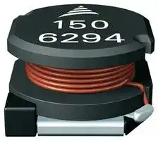
B82462A4104K.
INDUCTOR, UN-SHIELDED, 100UH, SMD
⚠️ Reference pricing provided. In case of supply shortages, we will connect you with our trusted procurement partners to ensure your project's continuity.
- Manufacturer: EPCOS
- Product type: SMD Power Inductors
- Inductance: 100µH
- Product Range: B82462A4 Series
- Product Width: 6mm
- Product Height: 3mm
- Product Length: 6mm
- DC Resistance Max: 1.28ohm
- RMS Current (Irms): 350mA
- Power Inductor Case: 6mm x 6mm x 3mm
- Inductance Tolerance: ± 10%
- Inductor Construction: Unshielded
- Saturation Current (Isat): 1.28A
| Delivery and price | |
|---|---|
| Units per pack | 2500 |
| Price | 0.905 € |
| Current stock | 10+ |
| Lead time | 30 days |
Datasheet

## **SMT power inductors**

Size 6.0 � 6.0 � 3.0 (mm)

**Series/Type: B82462A4** Date: June 2012

�� EPCOS AG 2012. Reproduction, publication and dissemination of this publication, enclosures hereto and the information contained therein without EPCOS’ prior express consent is prohibited.

~~LT~~ **SMT power inductors B82462A4 Size 6.0 x 6.0 x 3.0 (mm)**

**Rated inductance 1 ... 1000 μH Rated current 0.11 ... 3 A**

## **Construction**

- Ferrite core

- Winding: enamel copper wire

- Winding welded to terminals

## **Features**

- Temperature range up to +150 °C

- High rated current

- Low DC resistance

- Suitable for lead-free reflow soldering as referenced in JEDEC J-STD 020D

- Qualified to AEC-Q200

- RoHS-compatible

## **Applications**

- Filtering of supply voltages

- Coupling, decoupling

- DC/DC converters

- Automotive electronics

- Industrial electronics

## **Terminals**

- Base material CuSn6

- Layer composition Ag, Sn (lead-free)[1)]

- Electro-plated

## **Marking**

- Marking on component:

Manufacturer, L value (nH, coded),

   - L tolerance (coded), manufacturing date (YWWD)

- Minimum data on reel:

Manufacturer, ordering code, L value,

- quantity, date of packing

## **Delivery mode and packing unit**

- 12-mm blister tape, wound on 330-mm reel

- Packing unit: 2500 pcs./reel

1) Ni-barrier-plated terminals on request (B82462A4*50).

Please read _Cautions and warnings_ and _Important notes_ at the end of this document. **2** 06/12 -

## ~~LT~~ **SMT power inductors B82462A4 Size 6.0 x 6.0 x 3.0 (mm)**

## **Dimensional drawing and layout recommendation**

**==> picture [361 x 205] intentionally omitted <==**

**----- Start of picture text -----**<br>
VLAD 1.5 1.5<br>7<br>IND0469-B<br>1)<br>0.9±0.1<br>0.1<br>Marking<br>< /<br>6±0.2<br>1)<br>2.4<br>2±0.1<br>1)<br>0.15±0.03<br>3 max.<br>0.45±0.1<br>6 max.<br>**----- End of picture text -----**<br>


**==> picture [94 x 9] intentionally omitted <==**

**----- Start of picture text -----**<br>
Dimensions in mm<br>**----- End of picture text -----**<br>


**==> picture [128 x 22] intentionally omitted <==**

**----- Start of picture text -----**<br>
1) Soldering area<br>IND0471-F-E<br>**----- End of picture text -----**<br>


## **Taping and packing**

Blister tape

## Reel

**==> picture [479 x 181] intentionally omitted <==**

**----- Start of picture text -----**<br>
4±0.1 18.4 max. 13±0.2<br>Component 1.5+0.1 2±0.05<br>=o a tr zal<br>12.4 +1.5_0 62±1.5<br>|<br>Al S < TIS 1.6±0.1 ! — IND0350-S<br>3.45 max. 8±0.1<br>Direction of unreeling<br>IND0330-5-E<br>1.75±0.1 5.5±0.05<br>+0 2_<br>+0.3 0.1_ 330<br>12<br>7.5 max.<br>**----- End of picture text -----**<br>


Dimensions in mm

Please read _Cautions and warnings_ and _Important notes_ at the end of this document.

**3** 06/12

## ~~LT~~ **SMT power inductors B82462A4 Size 6.0 x 6.0 x 3.0 (mm)**

## **Technical data and measuring conditions**

|Rated inductance LR|Measured with impedance analyzer Agilent 4294A at|Measured with impedance analyzer Agilent 4294A at|
|---|---|---|
||frequencyfL, 0.1 V, +20 °C||
|Rated temperature TR|+85 °C||
|Rated current IR|Max. permissible DC with temperature increase of  40 K||
||at rated temperature||
|Saturation current Isat|Max. permissible DC with inductance decrease||
||L/L0of approx. 10%||
|DC resistance Rmax|Measured at +20 °C||
|Solderability (lead-free)|Dip and look method Sn95.5Ag3.8Cu0.7:||
||+(245 5) °C, (5 0.3) s||
||Wetting of soldering area 90%||
||(based on IEC 60068-2-58)||
|Resistance to solderingheat|+260 °C,40 s as referenced in JEDEC J-STD 020D||
|Climatic category|55/150/56(to IEC 60068-1)||
|Storage conditions|Mounted:<br>–55 °C … +150 °C||
||Packaged: –25 °C … +40 °C,|75% RH|
|Weight|Approx. 0.2g||


Please read _Cautions and warnings_ and _Important notes_ at the end of this document.

**4** 06/12 -

**B82462A4**

|LR<br>H<br>~~=FEEEE~~|Tolerance<br>~~=FEEEE~~|fL<br>MHz<br>~~=FEEEE~~|IR<br>A<br>~~=FEEEE~~|Isat<br>A<br>~~=FEEEE~~|Rmax<br>~~=FEEEE~~|Ordering code1)|
|---|---|---|---|---|---|---|
|1.0<br>1.5<br>2.2<br>~~=FEEEE~~|20%  M <br>~~^~~<br>~~=FEEEE~~|0.1<br>0.1<br>0.1<br>~~=FEEEE~~|3.00<br>2.60<br>2.30<br>~~=FEEEE~~|5.8<br>4.6<br>3.8<br>~~=FEEEE~~|0.024<br>0.030<br>0.042<br>~~=FEEEE~~|B82462A4102M000<br>B82462A4152M000<br>B82462A4222M000|
|3.3<br>4.7<br>6.8<br>10<br>~~=FEEEE~~||0.1<br>0.1<br>0.1<br>0.1<br>~~=FEEEE~~|2.00<br>1.65<br>1.40<br>1.15<br>~~=FEEEE~~|3.2<br>2.8<br>2.3<br>1.8<br>~~=FEEEE~~|0.060<br>0.080<br>0.10<br>0.14<br>~~=FEEEE~~|B82462A4332M000<br>B82462A4472M000<br>B82462A4682M000<br>B82462A4103M000|
|15<br>22<br>33|10%  K<br>~~^~~|0.1<br>0.1<br>0.1|0.90<br>0.80<br>0.63|1.5<br>1.28<br>1.04|0.21<br>0.26<br>0.42|B82462A4153K000<br>B82462A4223K000<br>B82462A4333K000|
|47<br>68<br>100||0.1<br>0.1<br>0.1|0.54<br>0.43<br>0.35|0.82<br>0.69<br>0.57|0.64<br>0.86<br>1.28|B82462A4473K000<br>B82462A4683K000<br>B82462A4104K000|
|150<br>220<br>330||0.1<br>0.1<br>0.1|0.29<br>0.24<br>0.20|0.49<br>0.40<br>0.34|1.76<br>2.72<br>3.90|B82462A4154K000<br>B82462A4224K000<br>B82462A4334K000|
|470<br>680<br>1000||0.1<br>0.1<br>0.1|0.17<br>0.14<br>0.11|0.28<br>0.23<br>0.18|5.60<br>8.00<br>13.00|B82462A4474K000<br>B82462A4684K000<br>B82462A4105K000|


Sample kit available. Ordering code: B82462X004 For more information refer to chapter “Sample kits”.

1) For Ni-barrier-plated terminals replace the last two digits “00” by “50”.

Please read _Cautions and warnings_ and _Important notes_ at the end of this document.

**5** 06/12 -

**SMT power inductors Size 6.0 x 6.0 x 3.0 (mm)**

**B82462A4**

**Impedance |Z| versus frequency f** measured with impedance analyzer Agilent 4294A, typical values at +20 °C

**==> picture [223 x 265] intentionally omitted <==**

**----- Start of picture text -----**<br>
10 6 IND0862-K<br>B82462A4<br>Ω a es<br>|Z| 10 5 TT<br>a<br>10 4 po|emer ieem RTTANAnat naman vk Cie Se RATiT<br>ALL Al Ny (YR<br>3<br>10 PTI pat ZIT<br>Co AAI ESAT NATIT<br>2<br>10 LIZ ANN be TIT TT NN<br>330 μH<br>rst ii 100 μH Hi<br>10 1 10 μH<br>2) 710<br>1 μH<br>10 0 SaV4<br>fs eee ace etl<br>10 _1 La WMI2 FL TUETHIE<br>10 3 10 4 10 5 10 6 10 7 Hz 10 8<br>— f<br>**----- End of picture text -----**<br>


**Inductance L versus DC load current IDC** measured with LCR meter Agilent 4275A, typical values at +20 °C

**==> picture [220 x 267] intentionally omitted <==**

**----- Start of picture text -----**<br>
IND0847-U<br>10 [3]<br>B82462A4<br>μH 330 μH FE<br>L ee<br>anH-CAH<br>10 2 ||—— 100 μH a ll<br>aa ee<br>a ee<br>|,<br>10 μH<br>10 1 eee<br>EHH<br>i |<br>0 CT 1 μH<br>10<br>Seena OOOO,Seee<br>LT LTTEETT<br>_ a lil<br>10 [1] 10 _1 10 [0] 10 [1] A 10 [2]<br>— IDC<br>**----- End of picture text -----**<br>


**Current derating Iop/IR versus ambient temperature TA** (rated temperature TR = +85 °C)

**==> picture [221 x 267] intentionally omitted <==**

**----- Start of picture text -----**<br>
IND0602-K<br>1.2<br>I<br>op<br>IR<br>1.0<br>0.8<br>TLEETLEET NEE<br>0.6<br>PEE NCE<br>0.4<br>0.2<br>REECE<br>0 0 20 40 60 80 100 120 ˚C 150<br>oy TA<br>**----- End of picture text -----**<br>


06/12

**6**

## ~~LT~~ **Cautions and warnings**

- Please note the recommendations in our Inductors data book (latest edition) and in the data sheets.

   - Particular attention should be paid to the derating curves given there.

   - The soldering conditions should also be observed. Temperatures quoted in relation to wave soldering refer to the pin, not the housing.

- If the components are to be washed varnished it is necessary to check whether the washing varnish agent that is used has a negative effect on the wire insulation, any plastics that are used, or on glued joints. In particular, it is possible for washing varnish agent residues to have a negative effect in the long-term on wire insulation.

   - Washing processes may damage the product due to the possible static or cyclic mechanical loads (e.g. ultrasonic cleaning). They may cause cracks to develop on the product and its parts, which might lead to reduced reliability or lifetime.

- The following points must be observed if the components are potted in customer applications: – Many potting materials shrink as they harden. They therefore exert a pressure on the plastic housing or core. This pressure can have a deleterious effect on electrical properties, and in extreme cases can damage the core or plastic housing mechanically.

   - It is necessary to check whether the potting material used attacks or destroys the wire insulation, plastics or glue.

   - The effect of the potting material can change the high-frequency behaviour of the components.

- Ferrites are sensitive to direct impact. This can cause the core material to flake, or lead to breakage of the core.

- Even for customer-specific products, conclusive validation of the component in the circuit can only be carried out by the customer.

Please read _Cautions and warnings_ and _Important notes_ at the end of this document.

**7** 06/12 -

~~LT~~ **Important notes**

The following applies to all products named in this publication:

1. Some parts of this publication contain **statements about the suitability of our products for certain areas of application** . These statements are based on our knowledge of typical requirements that are often placed on our products in the areas of application concerned. We nevertheless expressly point out **that such statements cannot be regarded as binding statements about the suitability of our products for a particular customer application.** As a rule, EPCOS is either unfamiliar with individual customer applications or less familiar with them than the customers themselves. For these reasons, it is always ultimately incumbent on the customer to check and decide whether an EPCOS product with the properties described in the product specification is suitable for use in a particular customer application.

2. We also point out that **in individual cases, a malfunction of electronic components or failure before the end of their usual service life cannot be completely ruled out in the current state of the art, even if they are operated as specified.** In customer applications requiring a very high level of operational safety and especially in customer applications in which the malfunction or failure of an electronic component could endanger human life or health (e.g. in accident prevention or life-saving systems), it must therefore be ensured by means of suitable design of the customer application or other action taken by the customer (e.g. installation of protective circuitry or redundancy) that no injury or damage is sustained by third parties in the event of malfunction or failure of an electronic component.

3. **The warnings, cautions and product-specific notes must be observed** .

4. In order to satisfy certain technical requirements, **some of the products described in this publication may contain substances subject to restrictions in certain jurisdictions (e.g. because they are classed as hazardous)** . Useful information on this will be found in our Material Data Sheets on the Internet (www.epcos.com/material). Should you have any more detailed questions, please contact our sales offices.

5. We constantly strive to improve our products. Consequently, **the products described in this publication may change from time to time** . The same is true of the corresponding product specifications. Please check therefore to what extent product descriptions and specifications contained in this publication are still applicable before or when you place an order.

We also **reserve the right to discontinue production and delivery of products** . Consequently, we cannot guarantee that all products named in this publication will always be available. The aforementioned does not apply in the case of individual agreements deviating from the foregoing for customer-specific products.

6. Unless otherwise agreed in individual contracts, **all orders are subject to the current version of the “General Terms of Delivery for Products and Services in the Electrical Industry” published by the German Electrical and Electronics Industry Association (ZVEI)** .

7. The trade names EPCOS, BAOKE, Alu-X, CeraDiode, CeraLink, CSMP, CSSP, CTVS, DeltaCap, DigiSiMic, DSSP, FilterCap, FormFit, MiniBlue, MiniCell, MKD, MKK, MLSC, MotorCap, PCC, PhaseCap, PhaseCube, PhaseMod, PhiCap, SIFERRIT, SIFI, SIKOREL, SilverCap, SIMDAD, SiMic, SIMID, SineFormer, SIOV, SIP5D, SIP5K, ThermoFuse, WindCap are **trademarks registered or pending** in Europe and in other countries. Further information will be found on the Internet at www.epcos.com/trademarks.

**8** 06/12 -
Updated at February 9, 2023
About Novapart
Novapart is a B2B electronic component broker specialising in stock shortages and cost reduction. We source hard-to-find parts and identify compliant alternatives across a catalogue of 410,000+ components from 500+ manufacturers.
Learn more →Stock Shortage Specialist
When a component is unavailable, discontinued or has an unacceptable lead time, we tap into our network of vetted European and Asian distributors to source what you need — without compromising on quality or traceability.
Request a quote →Compliant Alternatives
We identify pin-to-pin, electrically equivalent substitutes that meet the same certifications (RoHS, AEC-Q100, REACH) as your original specification — validated against datasheets, not just part numbers. Often at a lower cost.
BOM Analysis service →