
Image not available
Illustrative purposes only

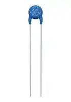
B72205S2301K101
TVS Varistor, 300 V, 385 V, B722 AdvanceD, 775 V, Disc 7mm, Metal Oxide Varistor (MOV)
⚠️ Reference pricing provided. In case of supply shortages, we will connect you with our trusted procurement partners to ensure your project's continuity.
- Manufacturer: EPCOS
- Product type: TVS Varistors
- Product Range: B722 AdvanceD
- Varistor Type: Metal Oxide Varistor (MOV)
- Voltage Rating VAC: 300V
- Voltage Rating VDC: 385V
- Varistor Case Style: Disc 7mm
- Clamping Voltage Vc Max: 775V
- Peak Energy (10/1000uS): 15J
- Operating Temperature Max: 85°C
- Operating Temperature Min: -40°C
- Peak Surge Current @ 8/20µs: 800A
| Delivery and price | |
|---|---|
| Units per pack | 50000 |
| Price | 0.138 € |
| Current stock | 50+ |
| Lead time | 7 days |
Datasheet

## **SIOV metal oxide varistors**

Leaded varistors, AdvanceD series

**Series/Type: B722*** Date: December 2011

© EPCOS AG 2015. Reproduction, publication and dissemination of this publication, enclosures hereto and the information contained therein without EPCOS' prior express consent is prohibited. EPCOS AG is a TDK Group Company.

**Leaded varistors B722*** ~~Lt~~ **AdvanceD series**

## **Construction**

Round varistor element, leaded

Coating: epoxy resin, flame-retardant to UL 94 V-0

## **Features**

High-energy AdvanceD series E2

High surge current ratings up to 10 kA

High energy ratings up to 440 J

Wide operating voltage range 130 … 680 VRMS PSpice models

## **Approvals**

UL CSA VDE CQC S05/07 (K11 … K460), S10/S14 (K11 … K680), S20 (K11 … K1000) IEC

## **Delivery mode**

Bulk (standard), taped versions on reel or in Ammo pack upon request. For further details refer chapter "Taping, packaging and lead configuration" for leaded varistors.

## **General technical data**

|Climatic category<br>to IEC 60068-1<br>Operating temperature<br>to IEC 61051<br>Storage temperature<br>Electric strength<br>to IEC 61051<br>Insulation resistance<br>to IEC 61051<br>Response time|40/85/56<br>40 ... + 85<br>40 ... +125<br>≥2.5<br>≥100<br>< 25|°C<br>°C<br>kVRMS<br>MΩ<br>ns|
|---|---|---|


Please read _Cautions and warnings_ and _Important notes_ at the end of this document.

Page 2 of 34

**Leaded varistors B722* AdvanceD series** ~~SEE~~ |

## **Electrical specifications and ordering codes Maximum ratings (TA = 85** ° **C)**

|**Maximum ratings (TA = 85A = 85 = 85**<br>~~—er~~|**Maximum ratings (TA = 85A = 85 = 85**°**C)**<br>~~er~~|~~er~~|~~er~~|~~er~~|~~er~~|~~er~~|
|---|---|---|---|---|---|---|
|Ordering code<br>~~—er~~|Type<br>(untaped)<br>SIOV-<br>~~er~~|VRMS<br>V<br>~~er~~|VDC<br>V<br>~~er~~|imax<br>(8/20 µs)<br>A<br>~~er~~|Wmax<br>(2 ms)<br>J<br>~~er~~|Pmax<br>W<br>~~er~~|
|VRMS= 130 V<br>~~—er~~|||||||
|B72205S2131K101<br>B72207S2131K101<br>B72210S2131K101<br>B72214S2131K101<br>B72220S2131K101<br>~~—~~<br>~~tt~~|S05K130E2<br>S07K130E2<br>S10K130E2<br>S14K130E2<br>S20K130E2<br><br>~~tt~~|130<br>130<br>130<br>130<br>130<br><br>~~tt~~|170<br>170<br>170<br>170<br>170<br><br>~~tt~~|800<br>1750<br>3500<br>6000<br>10000<br><br>~~tt~~|6.0<br>12.5<br>25.0<br>50.0<br>100.0<br><br>~~tt~~|0.10<br>0.25<br>0.40<br>0.60<br>1.00<br><br>~~tt~~|
|VRMS= 140 V<br>~~tt~~|||||||
|B72205S2141K101<br>B72207S2141K101<br>B72210S2141K101<br>B72214S2141K101<br>B72220S2141K101<br>~~tt~~|S05K140E2<br>S07K140E2<br>S10K140E2<br>S14K140E2<br>S20K140E2<br>~~tt~~|140<br>140<br>140<br>140<br>140<br>~~tt~~|180<br>180<br>180<br>180<br>180<br>~~tt~~|800<br>1750<br>3500<br>6000<br>10000<br>~~tt~~|6.5<br>13.5<br>27.5<br>55.0<br>110.0<br>~~tt~~|0.10<br>0.25<br>0.40<br>0.60<br>1.00<br>~~tt~~|
|VRMS= 150 V<br>~~tt~~|||||||
|B72205S2151K101<br>B72207S2151K101<br>B72210S2151K101<br>B72214S2151K101<br>B72220S2151K101<br>~~tt~~|S05K150E2<br>S07K150E2<br>S10K150E2<br>S14K150E2<br>S20K150E2<br>~~tt~~|150<br>150<br>150<br>150<br>150<br>~~tt~~|200<br>200<br>200<br>200<br>200<br>~~tt~~|800<br>1750<br>3500<br>6000<br>10000<br>~~tt~~|7.5<br>15.0<br>30.0<br>60.0<br>120.0<br>~~tt~~|0.10<br>0.25<br>0.40<br>0.60<br>1.00<br>~~tt~~|
|VRMS= 175 V<br>~~tt~~<br>~~tt~~|||||||
|B72205S2171K101<br>B72207S2171K101<br>B72210S2171K101<br>B72214S2171K101<br>B72220S2171K101<br>~~tt~~|S05K175E2<br>S07K175E2<br>S10K175E2<br>S14K175E2<br>S20K175E2<br>~~tt~~|175<br>175<br>175<br>175<br>175<br>~~tt~~|225<br>225<br>225<br>225<br>225<br>~~tt~~|800<br>1750<br>3500<br>6000<br>10000<br>~~tt~~|8.0<br>17.0<br>35.0<br>70.0<br>135.0<br>~~tt~~|0.10<br>0.25<br>0.40<br>0.60<br>1.00<br>~~tt~~|
|VRMS= 210 V<br>~~tt~~<br>~~tt~~|||||||
|B72205S2211K101<br>B72207S2211K101<br>B72210S2211K101<br>B72214S2211K101<br>B72220S2211K101<br>~~tt~~|S05K210E2<br>S07K210E2<br>S10K210E2<br>S14K210E2<br>S20K210E2<br>~~tt~~|210<br>210<br>210<br>210<br>210<br>~~tt~~|270<br>270<br>270<br>270<br>270<br>~~tt~~|800<br>1750<br>3500<br>6000<br>10000<br>~~tt~~|9.5<br>20.0<br>42.0<br>80.0<br>160.0<br>~~tt~~|0.10<br>0.25<br>0.40<br>0.60<br>1.00<br>~~tt~~|
|VRMS= 230 V<br>~~tt~~<br>~~—|tiiit~~|||||||
|B72205S2231K101<br>B72207S2231K101<br>B72210S2231K101<br>B72214S2231K101<br>B72220S2231K101<br>~~—|~~|S05K230E2<br>S07K230E2<br>S10K230E2<br>S14K230E2<br>S20K230E2<br>~~|tii~~|230<br>230<br>230<br>230<br>230<br>~~tii~~|300<br>300<br>300<br>300<br>300<br>~~tii~~|800<br>1750<br>3500<br>6000<br>10000<br>~~tiiit~~|11.0<br>23.0<br>45.0<br>90.0<br>180.0<br>~~it~~|0.10<br>0.25<br>0.40<br>0.60<br>1.00<br>~~it~~|


Please read _Cautions and warnings_ and _Important notes_ at the end of this document.

Page 3 of 34

## **Leaded varistors B722* AdvanceD series** ~~?D—=—~~

## **Characteristics (TA = 25** ° **C)**

|Ordering code<br>~~—LE~~|Vv<br>(1 mA)<br>V<br>~~LE~~|∆Vv<br>(1 mA)<br>%<br>~~LE~~|vc,max<br>(ic)<br>V<br>~~LE~~|ic<br>A<br>~~LE~~|Ctyp<br>(1 kHz)<br>pF<br>~~LE~~|
|---|---|---|---|---|---|
|VRMS= 130 V<br>~~—LE~~<br>~~_|~~||||||
|B72205S2131K101<br>B72207S2131K101<br>B72210S2131K101<br>B72214S2131K101<br>B72220S2131K101<br>~~—~~<br>~~_~~<br>~~tt~~|205<br>205<br>205<br>205<br>205<br><br>~~|~~<br>~~tt~~|±10<br>±10<br>±10<br>±10<br>±10<br><br>~~|~~<br>~~tt~~|340<br>340<br>340<br>340<br>340<br><br>~~tt~~|5.0<br>10.0<br>25.0<br>50.0<br>100.0<br><br>~~tt~~|135<br>245<br>500<br>880<br>1850<br><br>~~tt~~|
|VRMS= 140 V<br>~~_|~~<br>~~tt~~<br>~~_|~~||||||
|B72205S2141K101<br>B72207S2141K101<br>B72210S2141K101<br>B72214S2141K101<br>B72220S2141K101<br>~~_ ~~<br>~~_~~<br>~~tt~~|220<br>220<br>220<br>220<br>220<br> ~~|~~<br>~~|~~<br>~~tt~~|±10<br>±10<br>±10<br>±10<br>±10<br>~~|~~<br>~~|~~<br>~~tt~~|360<br>360<br>360<br>360<br>360<br>~~tt~~|5.0<br>10.0<br>25.0<br>50.0<br>100.0<br>~~tt~~|125<br>230<br>470<br>820<br>1700<br>~~tt~~|
|VRMS= 150 V<br>~~_|~~<br>~~tt~~<br>~~| tt~~||||||
|B72205S2151K101<br>B72207S2151K101<br>B72210S2151K101<br>B72214S2151K101<br>B72220S2151K101<br>~~_ ~~<br>~~|~~|240<br>240<br>240<br>240<br>240<br> ~~|~~<br>~~|~~|±10<br>±10<br>±10<br>±10<br>±10<br>~~|~~<br>~~| tt~~|395<br>395<br>395<br>395<br>395<br>~~tt~~|5.0<br>10.0<br>25.0<br>50.0<br>100.0<br>~~tt~~|115<br>210<br>430<br>750<br>1550<br>~~tt~~|
|VRMS= 175 V<br>~~| tt~~<br>~~_|~~<br>~~tt~~||||||
|B72205S2171K101<br>B72207S2171K101<br>B72210S2171K101<br>B72214S2171K101<br>B72220S2171K101<br>~~|~~<br>~~_~~<br>~~tt~~|270<br>270<br>270<br>270<br>270<br>~~|~~<br>~~|~~<br>~~tt~~|±10<br>±10<br>±10<br>±10<br>±10<br>~~| tt~~<br>~~|~~<br>~~tt~~|455<br>455<br>455<br>455<br>455<br>~~tt~~<br>~~tt~~|5.0<br>10.0<br>25.0<br>50.0<br>100.0<br>~~tt~~<br>~~tt~~|100<br>190<br>380<br>670<br>1350<br>~~tt~~<br>~~tt~~|
|VRMS= 210 V<br>~~_|~~<br>~~tt~~<br>~~| tt~~||||||
|B72205S2211K101<br>B72207S2211K101<br>B72210S2211K101<br>B72214S2211K101<br>B72220S2211K101<br>~~_ ~~<br>~~|~~|330<br>330<br>330<br>330<br>330<br> ~~|~~<br>~~|~~|±10<br>±10<br>±10<br>±10<br>±10<br>~~|~~<br>~~| tt~~|545<br>545<br>545<br>545<br>545<br>~~tt~~|5.0<br>10.0<br>25.0<br>50.0<br>100.0<br>~~tt~~|75<br>140<br>290<br>580<br>1100<br>~~tt~~|
|VRMS= 230 V<br>~~| tt~~<br>~~|} ttt~~||||||
|B72205S2231K101<br>B72207S2231K101<br>B72210S2231K101<br>B72214S2231K101<br>B72220S2231K101<br>~~|~~<br>~~|}~~|360<br>360<br>360<br>360<br>360<br>~~|~~<br>~~|}~~|±10<br>±10<br>±10<br>±10<br>±10<br>~~| tt~~<br>~~|} ttt~~|595<br>595<br>595<br>595<br>595<br>~~tt~~<br>~~ttt~~|5.0<br>10.0<br>25.0<br>50.0<br>100.0<br>~~tt~~<br>~~ttt~~|70<br>130<br>265<br>530<br>1000<br>~~tt~~<br>~~ttt~~|


Please read _Cautions and warnings_ and _Important notes_ at the end of this document.

Page 4 of 34

**Leaded varistors B722* AdvanceD series**

## **Electrical specifications and ordering codes Maximum ratings (TA = 85** ° **C)**

|**Electrical specifications and ordering codes**<br>**Maximum ratings (TA = 85A = 85 = 85**<br>~~es~~|**Electrical specifications and ordering codes**<br>**Maximum ratings (TA = 85A = 85 = 85**°**C)**<br>|**Electrical specifications and ordering codes**<br>|||||
|---|---|---|---|---|---|---|
|Ordering code<br>~~es~~|Type<br>(untaped)<br>SIOV-<br>|VRMS<br>V<br>|VDC<br>V<br>|imax<br>(8/20 µs)<br>A<br>|Wmax<br>(2 ms)<br>J<br>|Pmax<br>W<br>|
|VRMS= 250 V<br>~~es~~|||||||
|B72205S2251K101<br>B72207S2251K101<br>B72210S2251K101<br>B72214S2251K101<br>B72220S2251K101<br>~~es|~~|S05K250E2<br>S07K250E2<br>S10K250E2<br>S14K250E2<br>S20K250E2<br>~~|~~|250<br>250<br>250<br>250<br>250<br>~~|~~|320<br>320<br>320<br>320<br>320<br>~~|~~|800<br>1750<br>3500<br>6000<br>10000<br>~~|~~|12.0<br>25.0<br>50.0<br>100.0<br>195.0<br>~~|~~|0.10<br>0.25<br>0.40<br>0.60<br>1.00<br>~~|~~|
|VRMS= 275 V<br>~~|~~|||||||
|B72205S2271K101<br>B72207S2271K101<br>B72210S2271K101<br>B72214S2271K101<br>B72220S2271K101<br>~~|~~|S05K275E2<br>S07K275E2<br>S10K275E2<br>S14K275E2<br>S20K275E2<br>~~|~~|275<br>275<br>275<br>275<br>275<br>~~|~~|350<br>350<br>350<br>350<br>350<br>~~|~~|800<br>1750<br>3500<br>6000<br>10000<br>~~|~~|13.5<br>27.5<br>55.0<br>110.0<br>215.0<br>~~|~~|0.10<br>0.25<br>0.40<br>0.60<br>1.00<br>~~|~~|
|VRMS= 300 V<br>~~|~~|||||||
|B72205S2301K101<br>B72207S2301K101<br>B72210S2301K101<br>B72214S2301K101<br>B72220S2301K101<br>~~|~~|S05K300E2<br>S07K300E2<br>S10K300E2<br>S14K300E2<br>S20K300E2<br>~~|~~|300<br>300<br>300<br>300<br>300<br>~~|~~|385<br>385<br>385<br>385<br>385<br>~~|~~|800<br>1750<br>3500<br>6000<br>10000<br>~~|~~|15.0<br>30.0<br>60.0<br>125.0<br>250.0<br>~~|~~|0.10<br>0.25<br>0.40<br>0.60<br>1.00<br>~~|~~|
|VRMS= 320 V<br>~~|~~<br>~~_~~<br>~~||i}it~~<br>~~a~~|||||||
|B72207S2321K101<br>B72210S2321K101<br>B72214S2321K101<br>B72220S2321K101<br>~~_~~<br>~~|~~<br>~~a~~|S07K320E2<br>S10K320E2<br>S14K320E2<br>S20K320E2<br>~~_~~<br>~~||i}~~<br>|320<br>320<br>320<br>320<br>~~_~~<br>~~|i}~~<br>|420<br>420<br>420<br>420<br>~~_~~<br>~~|i}~~<br>|1750<br>3500<br>6000<br>10000<br>~~_~~<br>~~|i}it~~<br>|32.0<br>67.0<br>136.0<br>273.0<br>~~_~~<br>~~it~~<br>|0.25<br>0.40<br>0.60<br>1.00<br>~~_~~<br>~~it~~<br>|
|VRMS= 385 V<br>~~_~~<br>~~||i}it~~<br>~~a~~|||||||
|B72210S2381K101<br>B72214S2381K101<br>B72220S2381K101<br>~~_~~<br>~~|~~<br>~~a~~|S10K385E2<br>S14K385E2<br>S20K385E2<br>~~_~~<br>~~||i}~~<br>|385<br>385<br>385<br>~~_~~<br>~~|i}~~<br>|505<br>505<br>505<br>~~_~~<br>~~|i}~~<br>|3500<br>5000<br>10000<br>~~_~~<br>~~|i}it~~<br>|67.0<br>136.0<br>273.0<br>~~_~~<br>~~it~~<br>|0.40<br>0.60<br>1.00<br>~~_~~<br>~~it~~<br>|
|VRMS= 420 V<br>~~||i}it~~<br>~~a1.~~|||||||
|B72210S2421K101<br>B72214S2421K101<br>B72220S2421K101<br>~~|~~<br>~~a1.~~<br>~~es~~|S10K420E2<br>S14K420E2<br>S20K420E2<br>~~| |i}~~<br>~~1.~~|420<br>420<br>420<br>~~|i}~~<br>~~1.~~|560<br>560<br>560<br>~~|i}~~<br>~~1.~~|3500<br>5000<br>10000<br>~~|i} it~~<br>~~1.~~|67.0<br>136.0<br>273.0<br>~~it~~<br>~~1.~~|0.40<br>0.60<br>1.00<br>~~it~~<br>~~1.~~|
|VRMS= 460 V<br>~~1.~~<br>~~es~~|||||||
|B72210S2461K101<br>B72214S2461K101<br>B72220S2461K101<br>~~es~~|S10K460E2<br>S14K460E2<br>S20K460E2|460<br>460<br>460|615<br>615<br>615|3500<br>5000<br>10000|70.0<br>150.0<br>300.0|0.40<br>0.60<br>1.00|


Please read _Cautions and warnings_ and _Important notes_ at the end of this document.

Page 5 of 34

**Leaded varistors AdvanceD series**

**B722***

**Characteristics (TA = 25** ° **C)**

|Ordering code<br>~~__~~|Vv<br>(1 mA)<br>V<br>~~__~~|∆Vv<br>(1 mA)<br>%<br>~~__~~|vc,max<br>(ic)<br>V<br>~~__~~|ic<br>A<br>~~__~~|Ctyp<br>(1 kHz)<br>pF<br>~~__~~|
|---|---|---|---|---|---|
|VRMS= 250 V<br>~~__~~||||||
|B72205S2251K101<br>B72207S2251K101<br>B72210S2251K101<br>B72214S2251K101<br>B72220S2251K101<br>~~tt~~|390<br>390<br>390<br>390<br>390<br>~~tt~~|±10<br>±10<br>±10<br>±10<br>±10<br>~~tt~~|650<br>650<br>650<br>650<br>650<br>~~tt~~|5.0<br>10.0<br>25.0<br>50.0<br>100.0<br>~~tt~~|65<br>120<br>245<br>490<br>940<br>~~tt~~|
|VRMS= 275 V<br>~~tt~~||||||
|B72205S2271K101<br>B72207S2271K101<br>B72210S2271K101<br>B72214S2271K101<br>B72220S2271K101<br>~~tt~~|430<br>430<br>430<br>430<br>430<br>~~tt~~|±10<br>±10<br>±10<br>±10<br>±10<br>~~tt~~|710<br>710<br>710<br>710<br>710<br>~~tt~~|5.0<br>10.0<br>25.0<br>50.0<br>100.0<br>~~tt~~|60<br>110<br>220<br>440<br>850<br>~~tt~~|
|VRMS= 300 V<br>~~tt~~<br>~~_~~||||||
|B72205S2301K101<br>B72207S2301K101<br>B72210S2301K101<br>B72214S2301K101<br>B72220S2301K101<br>~~_~~|470<br>470<br>470<br>470<br>470<br>|±10<br>±10<br>±10<br>±10<br>±10<br>|775<br>775<br>775<br>775<br>775<br>|5.0<br>10.0<br>25.0<br>50.0<br>100.0<br>|55<br>100<br>200<br>400<br>780<br>|
|VRMS= 320 V<br>~~___|~~<br>~~||||~~||||||
|B72207S2321K101<br>B72210S2321K101<br>B72214S2321K101<br>B72220S2321K101<br>~~___|~~|510<br>510<br>510<br>510<br>~~__|~~<br>~~|~~|±10<br>±10<br>±10<br>±10<br>~~__|~~<br>~~||~~|840<br>840<br>840<br>840<br>~~__|~~<br>~~||~~|10.0<br>25.0<br>50.0<br>100.0<br>~~__|~~<br>~~||~~|90<br>185<br>370<br>720<br>~~__|~~<br>~~|~~|
|VRMS= 385 V<br>~~__|~~<br>~~||||~~<br>~~__~~||||||
|B72210S2381K101<br>B72214S2381K101<br>B72220S2381K101<br>~~__~~|620<br>620<br>620<br>~~|~~<br>~~__~~|±10<br>±10<br>±10<br>~~| |~~<br>~~__~~|1025<br>1025<br>1025<br>~~| |~~<br>~~__~~|25.0<br>50.0<br>100.0<br>~~| |~~<br>~~__~~|175<br>315<br>600<br>~~|~~<br>~~__~~|
|VRMS= 420 V<br>~~__~~<br>~~__~~||||||
|B72210S2421K101<br>B72214S2421K101<br>B72220S2421K101<br>~~__~~|680<br>680<br>680<br>~~__~~|±10<br>±10<br>±10<br>~~__~~|1120<br>1120<br>1120<br>~~__~~|25.0<br>50.0<br>100.0<br>~~__~~|165<br>290<br>550<br>~~__~~|
|VRMS= 460 V<br>~~__~~<br>~~a~~||||||
|B72210S2461K101<br>B72214S2461K101<br>B72220S2461K101<br>~~a~~|750<br>750<br>750<br>~~a~~|±10<br>±10<br>±10<br>~~a~~|1240<br>1240<br>1240<br>~~a~~|25.0<br>50.0<br>100.0<br>~~a~~|150<br>260<br>500<br>~~a~~|


Please read _Cautions and warnings_ and _Important notes_ at the end of this document.

Page 6 of 34

|**Leaded varistors**|**B722***|
|---|---|
|**AdvanceD series**||


## **Electrical specifications and ordering codes**

**Maximum ratings (TA = 85** ° **C)**

|Ordering code<br>~~|~~|Type<br>(untaped)<br>SIOV-<br>~~|~~|VRMS<br>V<br>~~| ||~~|VDC<br>V<br>~~||~~|imax<br>(8/20 µs)<br>A<br>~~||~~|Wmax<br>(2 ms)<br>J<br>~~||~~|Pmax<br>W<br>~~||~~|
|---|---|---|---|---|---|---|
|VRMS= 510 V<br>~~| ||~~|||||||
|B72210S2511K101<br>B72214S2511K101<br>B72220S2511K101<br>~~eee~~|S10K510E2<br>S14K510E2<br>S20K510E2<br>~~eee~~|510<br>510<br>510<br>~~eee~~|670<br>670<br>670<br>~~eee~~|3500<br>5000<br>10000<br>~~eee~~|80.0<br>165.0<br>325.0<br>~~eee~~|0.40<br>0.60<br>1.00<br>~~eee~~|
|VRMS= 550 V<br>~~eee~~<br>~~TTT~~|||||||
|B72210S2551K101<br>B72214S2551K101<br>B72220S2551K101<br>~~TTT~~|S10K550E2<br>S14K550E2<br>S20K550E2<br>~~TTT~~|550<br>550<br>550<br>~~TTT~~|745<br>745<br>745<br>~~TTT~~|3500<br>5000<br>10000<br>~~TTT~~|90.0<br>180.0<br>360.0<br>~~TTT~~|0.40<br>0.60<br>1.00<br>~~TTT~~|
|VRMS= 625 V<br>~~TTT~~|||||||
|B72210S2621K101<br>B72214S2621K101<br>B72220S2621K101<br>~~TTT~~|S10K625E2<br>S14K625E2<br>S20K625E2<br>~~TTT~~|625<br>625<br>625<br>~~TTT~~|825<br>825<br>825<br>~~TTT~~|3500<br>5000<br>10000<br>~~TTT~~|100.0<br>200.0<br>400.0<br>~~TTT~~|0.40<br>0.60<br>1.00<br>~~TTT~~|
|VRMS= 680 V<br>~~TTT~~<br>~~—|~~<br>~~Tt}~~<br>~~tf~~|||||||
|B72210S2681K101<br>B72214S2681K101<br>B72220S2681K101<br>~~—|~~<br>~~Tt}~~|S10K680E2<br>S14K680E2<br>S20K680E2<br>~~|~~<br>~~Tt}~~|680<br>680<br>680<br>~~Tt}~~|895<br>895<br>895<br>~~Tt}~~|3500<br>5000<br>10000<br>~~Tt}~~<br>~~tf~~|110.0<br>220.0<br>440.0<br>~~Tt}~~<br>~~tf~~|0.40<br>0.60<br>1.00<br>~~Tt}~~<br>~~tf~~|


Please read _Cautions and warnings_ and _Important notes_ at the end of this document.

Page 7 of 34

**Leaded varistors AdvanceD series**

**B722***

**Characteristics (TA = 25** ° **C)**

|Ordering code<br>~~Tt~~|Vv<br>(1 mA)<br>V<br>~~Tt~~|∆Vv<br>(1 mA)<br>%<br>~~Tt~~|vc,max<br>(ic)<br>V<br>~~Tt~~|ic<br>A<br>~~Tt~~|Ctyp<br>(1 kHz)<br>pF<br>~~Tt~~|
|---|---|---|---|---|---|
|VRMS= 510 V<br>~~Tt~~<br>~~ee~~<br>~~ee~~||||||
|B72210S2511K101<br>B72214S2511K101<br>B72220S2511K101<br>~~ee~~|820<br>820<br>820<br>~~ee~~|±10<br>±10<br>±10<br>~~ee~~|1355<br>1355<br>1355|25.0<br>50.0<br>100.0<br>~~ee~~|140<br>240<br>460<br>~~ee~~|
|VRMS= 550 V<br>~~ee~~<br>~~ee~~<br>~~ee~~||||||
|B72210S2551K101<br>B72214S2551K101<br>B72220S2551K101<br>~~ee~~|910<br>910<br>910<br>~~ee~~|±10<br>±10<br>±10<br>~~ee~~|1500<br>1500<br>1500<br>~~ee~~|25.0<br>50.0<br>100.0<br>~~ee~~|120<br>215<br>410<br>~~ee~~|
|VRMS= 625 V<br>~~ee~~<br>~~ee~~<br>~~ee~~||||||
|B72210S2621K101<br>B72214S2621K101<br>B72220S2621K101<br>~~ee~~|1000<br>1000<br>1000<br>~~ee~~|±10<br>±10<br>±10|1650<br>1650<br>1650<br>~~ee~~|25.0<br>50.0<br>100.0<br>~~ee~~|110<br>200<br>380<br>~~ee~~|
|VRMS= 680 V<br>~~ee~~<br>~~ee~~<br>~~—|~~<br>~~|~~<br>~~|~~<br>~~|fe~~||||||
|B72210S2681K101<br>B72214S2681K101<br>B72220S2681K101<br>~~—|~~|1100<br>1100<br>1100<br>~~|~~<br>~~|~~|±10<br>±10<br>±10<br>~~|~~<br>~~|~~|1815<br>1815<br>1815<br>~~|~~<br>~~|~~|25.0<br>50.0<br>100.0<br>~~|fe~~|100<br>180<br>340<br>~~fe~~|


Please read _Cautions and warnings_ and _Important notes_ at the end of this document.

Page 8 of 34

## **Leaded varistors AdvanceD series**

## **B722***

## **Dimensional drawings**

## **Weight**

|Nominal diameter<br>mm|VRMS<br>V|Weight<br>g|
|---|---|---|
|5<br>7<br>10<br>14<br>20|130 ... 300<br>130 ... 320<br>130 ... 680<br>130 ... 680<br>130 ... 680|0.4 ... 0.5<br>0.6 ... 0.8<br>1.2 ... 2.8<br>1.8 ... 4.8<br>3.3 ... 9.6|


The weight of varistors in between these voltage classes can be interpolated.

## **Dimensions**

|Ordering code|[e]±1<br>mm|a±1<br>mm|wmax<br>mm|thmax<br>mm|hmax<br>mm|lmin<br>mm|d±0.05<br>mm|
|---|---|---|---|---|---|---|---|
|VRMS= 130 V||||||||
|B72205S2131K101<br>B72207S2131K101<br>B72210S2131K101<br>B72214S2131K101<br>B72220S2131K101|5.0<br>5.0<br>7.5<br>7.5<br>10.0|1.6<br>1.6<br>1.8<br>1.9<br>2.0|7.0<br>9.0<br>12.0<br>15.5<br>21.5|3.9<br>3.9<br>4.5<br>4.6<br>5.0|8.5<br>11.0<br>14.5<br>18.5<br>25.5|25.0<br>25.0<br>25.0<br>25.0<br>25.0|0.6<br>0.6<br>0.8<br>0.8<br>1.0|
|VRMS= 140 V||||||||
|B72205S2141K101<br>B72207S2141K101<br>B72210S2141K101<br>B72214S2141K101<br>B72220S2141K101|5.0<br>5.0<br>7.5<br>7.5<br>10.0|1.7<br>1.7<br>1.9<br>2.0<br>2.1|7.0<br>9.0<br>12.0<br>15.5<br>21.5|4.0<br>4.0<br>4.6<br>4.7<br>5.1|8.5<br>11.0<br>14.5<br>18.5<br>25.5|25.0<br>25.0<br>25.0<br>25.0<br>25.0|0.6<br>0.6<br>0.8<br>0.8<br>1.0|
|VRMS= 150 V||||||||
|B72205S2151K101<br>B72207S2151K101<br>B72210S2151K101<br>B72214S2151K101<br>B72220S2151K101|5.0<br>5.0<br>7.5<br>7.5<br>10.0|1.8<br>1.8<br>2.0<br>2.1<br>2.2|7.0<br>9.0<br>12.0<br>15.5<br>21.5|4.1<br>4.1<br>4.7<br>4.8<br>5.2|8.5<br>11.0<br>14.5<br>18.5<br>25.5|25.0<br>25.0<br>25.0<br>25.0<br>25.0|0.6<br>0.6<br>0.8<br>0.8<br>1.0|
|VRMS= 175 V||||||||
|B72205S2171K101<br>B72207S2171K101<br>B72210S2171K101<br>B72214S2171K101<br>B72220S2171K101|5.0<br>5.0<br>7.5<br>7.5<br>10.0|2.0<br>2.0<br>2.2<br>2.2<br>2.3|7.0<br>9.0<br>12.0<br>15.5<br>21.5|4.3<br>4.3<br>4.9<br>4.9<br>5.3|8.5<br>11.0<br>14.5<br>18.5<br>25.5|25.0<br>25.0<br>25.0<br>25.0<br>25.0|0.6<br>0.6<br>0.8<br>0.8<br>1.0|


Please read _Cautions and warnings_ and _Important notes_ at the end of this document.

Page 9 of 34

|Ordering code|[e]±1<br>mm|a±1<br>mm|wmax<br>mm|thmax<br>mm|hmax<br>mm|lmin<br>mm|d±0.05<br>mm|
|---|---|---|---|---|---|---|---|
|VRMS= 210 V||||||||
|B72205S2211K101<br>B72207S2211K101<br>B72210S2211K101<br>B72214S2211K101<br>B72220S2211K101<br>~~tt~~|5.0<br>5.0<br>7.5<br>7.5<br>10.0<br>~~tt~~|1.7<br>1.7<br>1.9<br>1.9<br>2.2<br>~~tt~~|7.0<br>9.0<br>12.0<br>15.5<br>21.5<br>~~tt~~|4.2<br>4.2<br>5.0<br>5.0<br>5.4<br>~~tt~~|8.5<br>11.0<br>14.5<br>18.5<br>25.5<br>~~tt~~|25.0<br>25.0<br>25.0<br>25.0<br>25.0<br>~~tt~~|0.6<br>0.6<br>0.8<br>0.8<br>1.0<br>~~tt~~|
|VRMS= 230 V<br>~~tt~~||||||||
|B72205S2231K101<br>B72207S2231K101<br>B72210S2231K101<br>B72214S2231K101<br>B72220S2231K101<br>~~tt~~|5.0<br>5.0<br>7.5<br>7.5<br>10.0<br>~~tt~~|1.8<br>1.8<br>2.0<br>2.0<br>2.3<br>~~tt~~|7.0<br>9.0<br>12.0<br>15.5<br>21.5<br>~~tt~~|4.4<br>4.4<br>5.0<br>5.1<br>5.5<br>~~tt~~|8.5<br>11.0<br>14.5<br>18.5<br>25.5<br>~~tt~~|25.0<br>25.0<br>25.0<br>25.0<br>25.0<br>~~tt~~|0.6<br>0.6<br>0.8<br>0.8<br>1.0<br>~~tt~~|
|VRMS= 250 V<br>~~tt~~||||||||
|B72205S2251K101<br>B72207S2251K101<br>B72210S2251K101<br>B72214S2251K101<br>B72220S2251K101<br>~~tt~~|5.0<br>5.0<br>7.5<br>7.5<br>10.0<br>~~tt~~|1.9<br>1.9<br>2.1<br>2.1<br>2.4<br>~~tt~~|7.0<br>9.0<br>12.0<br>15.5<br>21.5<br>~~tt~~|4.5<br>4.5<br>5.2<br>5.2<br>5.7<br>~~tt~~|8.5<br>11.0<br>14.5<br>18.5<br>25.5<br>~~tt~~|25.0<br>25.0<br>25.0<br>25.0<br>25.0<br>~~tt~~|0.6<br>0.6<br>0.8<br>0.8<br>1.0<br>~~tt~~|
|VRMS= 275 V<br>~~tt~~<br>~~tt~~||||||||
|B72205S2271K101<br>B72207S2271K101<br>B72210S2271K101<br>B72214S2271K101<br>B72220S2271K101<br>~~tt~~|5.0<br>5.0<br>7.5<br>7.5<br>10.0<br>~~tt~~|2.0<br>2.0<br>2.2<br>2.2<br>2.6<br>~~tt~~|7.0<br>9.0<br>12.0<br>15.5<br>21.5<br>~~tt~~|4.6<br>4.6<br>5.4<br>5.4<br>5.8<br>~~tt~~|8.5<br>11.0<br>14.5<br>18.5<br>25.5<br>~~tt~~|25.0<br>25.0<br>25.0<br>25.0<br>25.0<br>~~tt~~|0.6<br>0.6<br>0.8<br>0.8<br>1.0<br>~~tt~~|
|VRMS= 300 V<br>~~tt~~<br>~~tt~~||||||||
|B72205S2301K101<br>B72207S2301K101<br>B72210S2301K101<br>B72214S2301K101<br>B72220S2301K101<br>~~tt~~|5.0<br>5.0<br>7.5<br>7.5<br>10.0<br>~~tt~~|2.1<br>2.1<br>2.3<br>2.3<br>2.8<br>~~tt~~|7.0<br>9.0<br>12.0<br>15.5<br>21.5<br>~~tt~~|4.7<br>4.7<br>5.6<br>5.6<br>6.1<br>~~tt~~|8.5<br>11.0<br>14.5<br>18.5<br>25.5<br>~~tt~~|25.0<br>25.0<br>25.0<br>25.0<br>25.0<br>~~tt~~|0.6<br>0.6<br>0.8<br>0.8<br>1.0<br>~~tt~~|
|VRMS= 320 V<br>~~tt~~<br>~~_|jj}|||~~||||||||
|B72207S2321K101<br>B72210S2321K101<br>B72214S2321K101<br>B72220S2321K101<br>~~_|~~|5.0<br>7.5<br>7.5<br>10.0<br>~~|jj}~~|2.3<br>2.4<br>2.4<br>2.9<br>~~jj}~~|9.0<br>12.0<br>15.5<br>21.5<br>~~jj}~~|4.6<br>5.8<br>5.8<br>6.2<br>~~jj}|||~~|11.0<br>15.0<br>19.0<br>25.5<br>~~|||~~|25.0<br>25.0<br>25.0<br>25.0<br>~~|||~~|0.6<br>0.8<br>0.8<br>1.0<br>~~|||~~|
|VRMS= 385 V<br>~~_|jj}|||~~<br>~~a~~||||||||
|B72210S2381K101<br>B72214S2381K101<br>B72220S2381K101<br>~~_ |~~<br>~~a~~|7.5<br>7.5<br>10.0<br>~~| jj}~~<br>~~a~~|3.3<br>3.4<br>3.9<br>~~jj}~~<br>~~a~~|12.0<br>15.5<br>21.5<br>~~jj}~~<br>~~a~~|7.1<br>7.1<br>7.6<br>~~jj} |||~~<br>~~a~~|15.0<br>19.0<br>26.0<br>~~|||~~<br>~~a~~|25.0<br>25.0<br>25.0<br>~~|||~~<br>~~a~~|0.8<br>0.8<br>1.0<br>~~|||~~<br>~~a~~|


Please read _Cautions and warnings_ and _Important notes_ at the end of this document.

Page 10 of 34

|Ordering code|[e]±1<br>mm|a±1<br>mm|wmax<br>mm|thmax<br>mm|hmax<br>mm|lmin<br>mm|d±0.05<br>mm|
|---|---|---|---|---|---|---|---|
|VRMS= 420 V<br>~~| Tt~~||||||||
|B72210S2421K101<br>B72214S2421K101<br>B72220S2421K101<br>~~|~~|7.5<br>7.5<br>10.0<br>~~|~~|3.5<br>3.6<br>4.2<br>~~|~~<br>~~|~~|12.0<br>15.5<br>21.5<br>~~|~~<br>~~| Tt~~|7.4<br>7.5<br>7.9<br>~~|~~<br>~~Tt~~|15.0<br>19.0<br>26.0<br>~~|~~<br>~~Tt~~|25.0<br>25.0<br>25.0<br>~~|~~<br>~~Tt~~|0.8<br>0.8<br>1.0<br>~~|~~<br>~~Tt~~|
|VRMS= 460 V<br>~~|~~<br>~~| Tt~~<br>~~tT~~<br>~~|| tt~~||||||||
|B72210S2461K101<br>B72214S2461K101<br>B72220S2461K101<br>~~tT~~|7.5<br>7.5<br>10.0<br>~~tT~~<br>~~|~~|3.7<br>3.8<br>4.5<br>~~tT~~<br>~~||~~|12.0<br>15.5<br>21.5<br>~~tT~~<br>~~| tt~~|7.7<br>7.8<br>8.2<br>~~tT~~<br>~~tt~~|15.0<br>19.0<br>26.0<br>~~tT~~<br>~~tt~~|25.0<br>25.0<br>25.0<br>~~tT~~<br>~~tt~~|0.8<br>0.8<br>1.0<br>~~tT~~<br>~~tt~~|
|VRMS= 510 V<br>~~tT~~<br>~~| | tt~~<br>~~| tt~~||||||||
|B72210S2511K101<br>B72214S2511K101<br>B72220S2511K101<br>~~|~~|7.5<br>7.5<br>10.0<br>~~|~~|4.0<br>4.0<br>4.6<br>~~|~~<br>~~|~~|12.0<br>15.5<br>21.5<br>~~|~~<br>~~| tt~~|8.0<br>8.1<br>8.6<br>~~|~~<br>~~tt~~|15.0<br>19.0<br>26.0<br>~~|~~<br>~~tt~~|25.0<br>25.0<br>25.0<br>~~|~~<br>~~tt~~|0.8<br>0.8<br>1.0<br>~~|~~<br>~~tt~~|
|VRMS= 550 V<br>~~|~~<br>~~| tt~~<br>~~TT~~<br>~~| tt~~<br>~~—~~||||||||
|B72210S2551K101<br>B72214S2551K101<br>B72220S2551K101<br>~~TT~~<br>~~—~~|7.5<br>7.5<br>10.0<br>~~TT~~<br>|4.3<br>4.7<br>4.8<br>~~TT~~<br>~~|~~<br>|12.0<br>15.5<br>21.5<br>~~TT~~<br>~~| tt~~<br>|8.4<br>8.5<br>9.0<br>~~TT~~<br>~~tt~~|15.0<br>19.0<br>26.0<br>~~TT~~<br>~~tt~~|25.0<br>25.0<br>25.0<br>~~TT~~<br>~~tt~~|0.8<br>0.8<br>1.0<br>~~TT~~<br>~~tt~~|
|VRMS= 625 V<br>~~TT~~<br>~~| tt~~<br>~~—fT||~~<br>~~Tt~~||||||||
|B72210S2621K101<br>B72214S2621K101<br>B72220S2621K101<br>~~—fT~~<br>~~Tt~~|7.5<br>7.5<br>10.0<br>~~fT|~~<br>~~Tt~~|5.0<br>5.1<br>5.4<br>~~|~~<br>~~||~~<br>~~Tt~~|12.0<br>15.5<br>21.5<br>~~| tt~~<br>~~|~~<br>~~Tt~~|8.8<br>8.9<br>9.4<br>~~tt~~<br>~~Tt~~|15.0<br>19.0<br>26.0<br>~~tt~~<br>~~Tt~~|25.0<br>25.0<br>25.0<br>~~tt~~<br>~~Tt~~|0.8<br>0.8<br>1.0<br>~~tt~~<br>~~Tt~~|
|VRMS= 680 V<br>~~| tt~~<br>~~— fT | |~~<br>~~Tt~~<br>~~—itttttft~~||||||||
|B72210S2681K101<br>B72214S2681K101<br>B72220S2681K101<br>~~—itt~~|7.5<br>7.5<br>10.0<br>~~itt~~|5.4<br>5.5<br>5.8<br>~~itt~~|12.0<br>15.5<br>21.5<br>~~ittttt~~|9.2<br>9.3<br>9.8<br>~~ttt~~|15.0<br>19.0<br>26.0<br>~~ttt~~|25.0<br>25.0<br>25.0<br>~~tttft~~|0.8<br>0.8<br>1.0<br>~~ft~~|


Please read _Cautions and warnings_ and _Important notes_ at the end of this document.

Page 11 of 34

**Leaded varistors B722* AdvanceD series** ~~0_———~~

## **Reliability data**

|**Reliability data**|||
|---|---|---|
|Test|Test methods/conditions<br>~~pO~~|Requirement|
|Varistor voltage|The voltage between two terminals with<br>the specified measuring current applied<br>is called VV (1 mADC@ 0.2 ... 2 s).|To meet the specified value|
|Clamping voltage|The maximum voltage between two<br>terminals with the specified standard<br>impulse current(8/20µs)applied.|To meet the specified value|
|Endurance at upper<br>category temperature|1000 h at UCT<br>After having continuously applied the<br>maximum allowable AC voltage at UCT<br>±2°C for 1000 h, the specimen shall be<br>stored at room temperature and normal<br>humidity for 1 to 2 h.<br>Thereafter, the change of VVshall be<br>measured.||∆V/V (1 mA)|≤10%|
|Surge current derating,<br>8/20µs|10 surge currents (8/20µs), unipolar,<br>interval 30 s, amplitude corresponding<br>to derating curve for 10 impulses at<br>20µs||∆V/V (1 mA)|≤10%<br>(measured in direction of<br>surge current)<br>No visible damage|
|Surge current derating,<br>2 ms|10 surge currents (2 ms), unipolar,<br>interval 120 s, amplitude corresponding<br>to derating curve for 10 impulses at<br>2 ms||∆V/V (1 mA)|≤10%<br>(measured in direction of<br>surge current)<br>No visible damage|
|Electric strength|IEC 61051-1, test 4.9.2<br>Metal balls method, 2500 VRMS, 60 s<br>The varistor is placed in a container<br>holding 1.6±0.2 mm diameter metal<br>balls such that only the terminations of<br>the varistor are protruding.<br>The specified voltage shall be applied<br>between both terminals of the specimen<br>connected together and the electrode<br>inserted between the metal balls.|No breakdown|


Please read _Cautions and warnings_ and _Important notes_ at the end of this document.

Page 12 of 34

|Test|Test methods/conditions|Requirement|
|---|---|---|
|Climatic sequence|The specimen shall be subjected to:<br>a) dry heat at UCT, 16 h, IEC<br>60068-2-2, test Ba<br>b) damp heat, 1st cycle:<br>55°C, 93% r. H., 24 h, IEC<br>60068-2-30, test Db<br>c) cold, LCT, 2 h, IEC 60068-2-1, test<br>Aa<br>d) damp heat, additional 5 cycles:<br>55°C/25°C, 93% r. H., 24 h/cycle,<br>IEC 60068-2-30, test Db.<br>Then the specimen shall be stored at<br>room temperature and normal humidity<br>for 1 to 2 h.<br>Thereafter, the change of VVshall be<br>measured. Thereafter, insulation resis-<br>tance Rinsshall be measured at V = 500<br>V.||∆V/V (1 mA)|≤10%<br>Rins≥100 MΩ|
|Rapid change of<br>temperature|IEC 60068-2-14, test Na, LCT/UCT,<br>dwell time 30 min, 5 cycles||∆V/V (1 mA)|≤5%<br>No visible damage|
|Damp heat, steady state|IEC 60068-2-78, test Ca<br>The specimen shall be subjected to<br>40±2°C, 90 to 95% r. H. for 56 days<br>without load / with 10% of the maxi-<br>mum continuous DC operating voltage<br>VDC. Then stored at room temperature<br>and normal humidity for 1 to 2 h.<br>Thereafter, the change of VVshall be<br>measured. Thereafter, insulation resis-<br>tance Rinsshall be measured at V = 500<br>V(insulated varistors only).||∆V/V (1 mA)|≤10%<br>Rins≥100 MΩ|


Please read _Cautions and warnings_ and _Important notes_ at the end of this document.

Page 13 of 34

|Test|Test methods/conditions|Requirement|
|---|---|---|
|Solderability|IEC 60068-2-20, test Ta,<br>method 1 with modified conditions for<br>lead-free solder alloys: 245°C, 3 s:<br>After dipping the terminals to a depth of<br>approximately 3 mm from the body in a<br>soldering bath of 245°C for 3 s, the<br>terminals shall be visually examined.|The inspection shall be<br>carried out under adequate<br>light with normal eyesight or<br>with the assistance of a<br>magnifier capable of giving<br>a magnification of 4 to<br>10 times. The dipped<br>surface shall be covered<br>with a smooth and bright<br>solder coating with no more<br>than small amounts of<br>scattered imperfections<br>such as pinholes or<br>un-wetted or de-wetted<br>areas. These imperfections<br>shall not be concentrated in<br>one area.|
|Resistance to soldering<br>heat|IEC 60068-2-20, test Tb, method 1A,<br>260°C, 10 s:<br>Each lead shall be dipped into a solder<br>bath having a temperature of 260±5°C<br>to a point 2.0 to 2.5 mm from the body<br>of the specimen, be held there for<br>10±1 s and then be stored at room<br>temperature and normal humidity for<br>1 to 2 h.<br>The change of VVshall be measured<br>and the specimen shall be visually<br>examined.||∆V/V (1 mA)|≤5%<br>No visible damage|
|Tensile strength|IEC 60068-2-21, test Ua1<br>After gradually applying the force<br>specified below and keeping the unit<br>fixed for 10 s, the terminal shall be<br>visually examined for any damage.<br>Force for wire diameter:<br>0.6 mm = 10 N<br>0.8 mm = 10 N<br>1.0 mm = 20 N||∆V/V (1 mA)|≤5%<br>No break of solder joint,<br>no wire break|


Please read _Cautions and warnings_ and _Important notes_ at the end of this document.

Page 14 of 34

|Test|Test methods/conditions|Requirement|
|---|---|---|
|Vibration|IEC 60068-2-6, test Fc, method B4<br>Frequency range:<br>Amplitude:<br>Duration:<br>Pulse:<br>10 … 55 Hz<br>0.75 mm or 98 m/s2<br>6 h (3 · 2 h)<br>sine wave<br>After repeatedly applying a single<br>harmonic vibration according to the<br>table above.<br>The change of VVshall be measured<br>and the specimen shall be visually<br>examined.||∆V/V (1 mA)|≤5%<br>No visible damage|
|Bump|IEC 60068-2-29, test Eb<br>Pulse duration:<br>Max. acceleration:<br>Number of bumps:<br>Pulse:<br>6 ms<br>400 m/s2<br>4000<br>half sine||∆V/V (1 mA)|≤5%<br>No visible damage|
|Fire hazard|IEC 60695-11-5 (needle flame test)<br>Severity: vertical 10 s|5 s max.|


## **Note:**

UCT = Upper category temperature LCT = Lower category temperature Rins = Insulation resistance

Please read _Cautions and warnings_ and _Important notes_ at the end of this document.

Page 15 of 34

**Leaded varistors AdvanceD series**

**B722***

## **v/i characteristics**

v = f (i) - for explanation of the characteristics refer to "General technical information", 1.6.3 A = Leakage current, B = Protection level } for worst-case varistor tolerances

**SIOV-S05 ... E2**

**SIOV-S07 ... E2**

Please read _Cautions and warnings_ and _Important notes_ at the end of this document.

Page 16 of 34

**Leaded varistors AdvanceD series**

**B722***

## **v/i characteristics**

v = f (i) - for explanation of the characteristics refer to "General technical information", 1.6.3 A = Leakage current, B = Protection level } for worst-case varistor tolerances

**SIOV-S10 ... E2**

**SIOV-S14 ... E2**

Please read _Cautions and warnings_ and _Important notes_ at the end of this document.

Page 17 of 34

**Leaded varistors AdvanceD series**

**B722***

## **v/i characteristics**

v = f (i) - for explanation of the characteristics refer to "General technical information", 1.6.3 A = Leakage current, B = Protection level } for worst-case varistor tolerances

**SIOV-S20 ... E2**

Please read _Cautions and warnings_ and _Important notes_ at the end of this document.

Page 18 of 34

**Leaded varistors AdvanceD series**

**B722***

## **Derating curves**

Maximum surge current imax = f (tr, pulse train)

For explanation of the derating curves refer to "General technical information", section 1.8.1

## **SIOV-S05K130 ... K300E2**

**SIOV-S07K130 ... K320E2**

Please read _Cautions and warnings_ and _Important notes_ at the end of this document.

Page 19 of 34

**Leaded varistors AdvanceD series**

**B722***

## **Derating curves**

Maximum surge current imax = f (tr, pulse train) For explanation of the derating curves refer to "General technical information", section 1.8.1

**SIOV-S10K130 ... K320E2**

**SIOV-S10K385 ... K680E2**

Please read _Cautions and warnings_ and _Important notes_ at the end of this document.

Page 20 of 34

**Leaded varistors AdvanceD series**

**B722***

## **Derating curves**

Maximum surge current imax = f (tr, pulse train)

For explanation of the derating curves refer to "General technical information", section 1.8.1

## **SIOV-S14K130 ... K320E2**

**SIOV-S14K385 ... K680E2**

Please read _Cautions and warnings_ and _Important notes_ at the end of this document.

Page 21 of 34

**Leaded varistors AdvanceD series**

**B722***

## **Derating curves**

Maximum surge current imax = f (tr, pulse train) For explanation of the derating curves refer to "General technical information", section 1.8.1

## **SIOV-S20K130 ... K320E2**

**SIOV-S20K385 ... K680E2**

Please read _Cautions and warnings_ and _Important notes_ at the end of this document.

Page 22 of 34

**Leaded varistors B722* AdvanceD series**

## **Taping, packaging and lead configuration**

**1 EPCOS ordering code system**

## **For leaded varistors**

**==> picture [334 x 368] intentionally omitted <==**

**----- Start of picture text -----**<br>
B722 10 S 2 271 K 1 0 1<br>Monolithic<br>varistor<br>Nominal<br>disc diameter<br>Design:<br>S  =  Leaded varistor<br>T = ThermoFuse<br>F = Fail-safe varistor<br>Q = EnergetiQ<br>Series:<br>0 = StandarD<br>1 = Automotive<br>2 = AdvanceD<br>3 = SuperioR<br>4 = SuperioR<br>Max. AC operating voltage:<br>271 = 27 10 [1] = 275 VAC<br>140 = 14 10 [0] = 14 VAC<br>141 = 14 10 [1] = 140 VAC<br>Tolerance of varistor voltage:<br>K =  ± 10%<br>J =  ± 5%<br>S = Special tolerance<br>Lead configuration:<br>1 = Straight leads<br>2 thru 5 = Kinked form<br>Packaging:<br>0 = Bulk,<br>1 thru 7 = Taping style<br>Internal coding:<br>1 = Standard<br>**----- End of picture text -----**<br>


Please read _Cautions and warnings_ and _Important notes_ at the end of this document.

Page 23 of 34

|**Leaded varistors**<br>**AdvanceD series**|**B722***|
|---|---|


**2 Taping and packaging of leaded varistors**

Tape packaging for lead spacing [é] = 5 fully conforms to IEC 60286-2, while for lead spacings [e] = 7.5 and 10 the taping mode is based on this standard.

## **2.1 Taping in accordance with IEC 60286-2 for lead spacing 5.0 mm**

## **2.2 Taping based on IEC 60286-2 for lead spacing 7.5 and 10 mm**

Please read _Cautions and warnings_ and _Important notes_ at the end of this document.

Page 24 of 34

## **Leaded varistors B722* AdvanceD series** ~~SEE~~ |

|Sym-<br>bol|= 5.0<br>~~ete}~~|Tolerance<br>~~ete}~~|= 7.5<br>~~ete}~~|Tolerance<br>~~ete}|}~~|= 10.0<br>~~|}~~|Tolerance<br>~~|}~~|Remarks|
|---|---|---|---|---|---|---|---|
|w<br>th<br>d|0.6<br>~~ete}~~|max.<br>max.<br>±0.05<br>~~ete}~~|0.8<br>~~ete}~~|max.<br>max.<br>±0.05<br>~~ete} |}~~|1.0<br>~~|}~~|max.<br>max.<br>±0.05<br>~~|}~~|see tables in<br>each series<br>under<br>"Dimensions"|
|P0<br>P1|12.7<br>3.85|±0.3<br>±0.7|12.71)<br>8.95|±0.3<br>±0.8|12.7<br>7.7|±0.3<br>±0.8|±1 mm/20<br>sprocket holes|
|F<br>∆h<br>∆p|5.0<br>0<br>0|+0.6/ 0.1<br>±2.0<br>±1.3|7.5<br>±0.8<br>depends on s<br>0<br>±2.0||10.0<br>±0.8<br>depends on s<br>0<br>±2.0||measured at<br>top of compo-<br>nent body|
|W<br>W0<br>W1<br>W2|18.0<br>5.5<br>9.0<br>3.0|±0.5<br>min.<br>±0.5<br>max.|18.0<br>11.0<br>9.0<br>3.0|±0.5<br>min.<br>+0.75/ 0.5<br>max.|18.0<br>11.0<br>9.0<br>3.0|±0.5<br>min.<br>+0.75/ 0.5<br>max.|Peel-off<br>force<br>>5 N|
|H<br>H0<br>H1|18.0<br>16.0<br>(18.0)<br>32.2|+2.0/ 0<br>±0.5<br>max.|18.0<br>16.0<br>(18.0)<br>45.0|+2.0/ 0<br>±0.5<br>max.|18.0<br>16.0<br>45.0|+2.0/ 0<br>±0.5<br>max.|2)<br>3)|
|D0<br>t<br>L<br>l|4.0<br>0.9<br>11.0<br>4.0|±0.2<br>max.<br>max.<br>max.|4.0<br>0.9<br>11.0|±0.2<br>max.<br>max.|4.0<br>0.9<br>11.0|±0.2<br>max.<br>max.|without lead|


1) Taping with P0 = 15.0 mm upon request

2) Applies only to uncrimped types

3) Applies only to crimped types (H0 = 18 upon request)

Please read _Cautions and warnings_ and _Important notes_ at the end of this document.

Page 25 of 34

**Leaded varistors B722* AdvanceD series** ~~0_———~~

## **2.4 Taping mode** Example: B72210S0271K1 ~~LJ~~ **5** 1 | Digit 14

|Digit 14|Taping<br>mode|Reel type|Seating plane height H0<br>for crimped types<br>mm|Seating plane height H<br>for uncrimped types<br>mm|Pitch distance<br>P0<br>mm|
|---|---|---|---|---|---|
|0<br>1<br>2<br>3<br>4<br>5<br>6<br>7|G<br>G2<br>G3<br>G4<br>G5<br>GA<br>G2A|Bulk<br>I<br>I<br>II<br>II<br>III<br>Ammo pack<br>Ammopack|16<br>18<br>16<br>18<br>16<br>16<br>18|18<br>18<br>18<br>18|12.7<br>12.7<br>12.7<br>12.7<br>12.7<br>12.7<br>12.7|


Please read _Cautions and warnings_ and _Important notes_ at the end of this document.

Page 26 of 34

|**Leaded varistors**|**B722***|
|---|---|
|**AdvanceD series**||


## **2.5 Reel dimension**

**Dimensions** (in mm)

|**Dimensions**(in mm)|(in mm)||||
|---|---|---|---|---|
|Reel type|d|f|n|w|
|I<br>II<br>III|360 max.<br>360 max.<br>500 max.|31±1<br>31±1<br>23±1|approx. 45<br>approx. 55<br>approx. 59|54 max.<br>64 max.<br>72 max.|


If reel type III is not compatible with insertion equipment because of its large diameter, nominal disk diameter 10 mm and 14 mm can be supplied on reel II upon request (taping mode G3).

## **2.6 Ammo pack dimensions**

Please read _Cautions and warnings_ and _Important notes_ at the end of this document.

Page 27 of 34

**Leaded varistors AdvanceD series**

**B722***

## **3 Lead configuration**

Straight leads are standard for disk varistors. Other lead configurations as crimp style or customer-specific lead wire length according to 3.1, 3.2, 3.3 and 3.4 are optional. Crimped leads (non-standard) are differently crimped for technical reasons; the individual crimp styles are denoted by consecutive numbers (S, S2 through S5) as shown in the dimensional drawings below.

The crimp styles of the individual types can be seen from the type designation in the ordering tables.

## **3.1 Crimp style mode**

> Example: B72210S0271K ~~LJ~~ **5** 01 | Digit 13

**==> picture [259 x 94] intentionally omitted <==**

**----- Start of picture text -----**<br>
||||
|---|---|---|
|Digit 13 of ordering code|Crimp style|Figure|
|1|Standard, straight leads|1|
|2|S2|2|
|3|S3|3|
|4|S4|4|
|5|S5|5|
|Available upon request|
|Internal coding|6|

**----- End of picture text -----**<br>


## **3.2 Standard leads and non-standard crimp styles**

**Standard, straight leads**

**Non-standard, Non-standard, crimp style S2 crimp style S3**

**Figure 1**

**Figure 2**

**==> picture [32 x 9] intentionally omitted <==**

**----- Start of picture text -----**<br>
Figure 3<br>**----- End of picture text -----**<br>


Please read _Cautions and warnings_ and _Important notes_ at the end of this document.

Page 28 of 34

|**Leaded varistors**|**B722***|
|---|---|
|**AdvanceD series**||


## **Non-standard, crimp style S4 Non-standard, crimp style S5**

**Figure 4**

**Figure 5**

## **3.3 Component height (hmax) for crimped versions (non-standard)**

Due to technical reasons the component height (hmax) increases if a crimp is added. The maximum height of the crimped component can be found in the table below.

|Nominal diameter<br>mm|VRMS<br>V<br>Crimp style|Crimp style|mm|hmax<br>mm|
|---|---|---|---|---|
|5<br>5<br>7<br>7<br>10<br>10<br>10<br>10<br>10<br>10<br>10<br>14<br>14<br>14<br>14<br>14<br>20<br>20|11 ... 175<br>S2<br>210 ... 460<br>S3<br>11 ... 175<br>S2<br>210 ... 460<br>S3<br>11 ... 300<br>S5<br>320 ... 460<br>S3/S5<br>510<br>S3/S5<br>Automotive<br>S5<br>Automotive (D1 types)<br>S5<br>11 ... 175<br>S4<br>210 ... 460<br>S3<br>11 ... 300<br>S5<br>320 ... 460<br>S3/S5<br>510<br>S3/S5<br>Automotive<br>S5<br>Automotive (D1 types)<br>S5<br>11 ... 320<br>S5<br>385 ... 510<br>S5|S2<br>S3<br>S2<br>S3<br>S5<br>S3/S5<br>S3/S5<br>S5<br>S5<br>S4<br>S3<br>S5<br>S3/S5<br>S3/S5<br>S5<br>S5<br>S5<br>S5|5.0<br>5.0<br>5.0<br>5.0<br>7.5<br>7.5<br>7.5<br>7.5<br>7.5<br>5.0<br>5.0<br>7.5<br>7.5<br>7.5<br>7.5<br>7.5<br>10.0<br>10.0|10.0<br>10.0<br>12.0<br>12.0<br>15.5<br>16.5<br>17.5<br>17.0<br>16.0<br>16.5<br>16.5<br>20.0<br>20.0<br>21.5<br>21.0<br>20.0<br>27.0<br>27.5|


Please read _Cautions and warnings_ and _Important notes_ at the end of this document.

Page 29 of 34

**Leaded varistors AdvanceD series**

**B722***

## **3.4 Trimmed leads (non-standard)**

Varistors with cut leads available upon request.

Lead length tolerances: Straight leads +/ 1.0 mm Crimped leads +/ 0.8 mm Minimum lead length 3.5 mm

**Figure 6**

Please read _Cautions and warnings_ and _Important notes_ at the end of this document.

Page 30 of 34

**Leaded varistors B722* AdvanceD series** ~~SEE~~ |

## **Cautions and warnings**

## **General**

1. EPCOS metal oxide varistors are designed for specific applications and should not be used for purposes not identified in our specifications, application notes and data books unless otherwise agreed with EPCOS during the design-in-phase.

2. Ensure suitability of SIOVs through reliability testing during the design-in phase. SIOVs should be evaluated taking into consideration worst-case conditions.

3. For applications of SIOVs in line-to-ground circuits based on various international and local standards there are restrictions existing or additional safety measures required.

## **Storage**

1. Store SIOVs only in original packaging. Do not open the package before storage.

2. Storage conditions in original packaging: Storage temperature: 25 ° C ... +45 ° C, Relative humidity: <75% annual average, <95% on maximum 30 days a year.

Dew precipitation: is to be avoided.

3. Avoid contamination of an SIOV's during storage, handling and processing.

4. Avoid storage of SIOVs in harmful environments that can affect the function during long-term operation (examples given under operation precautions).

5. The SIOV type series should be soldered within the time specified: SIOV-S, -Q, -LS, -B, -SFS 24 months ETFV 12 months.

## **Handling**

1. SIOVs must not be dropped.

2. Components must not be touched with bare hands. Gloves are recommended.

3. Avoid contamination of the surface of SIOV electrodes during handling, be careful of the sharp edge of SIOV electrodes.

## **Soldering (where applicable)**

1. Use rosin-type flux or non-activated flux.

2. Insufficient preheating may cause ceramic cracks.

3. Rapid cooling by dipping in solvent is not recommended.

4. Complete removal of flux is recommended.

Please read _Cautions and warnings_ and _Important notes_ at the end of this document.

Page 31 of 34

|**Leaded varistors**<br>**B722***<br>**AdvanceD series**<br>~~0_———~~|
|---|


## **Mounting**

1. Potting, sealing or adhesive compounds can produce chemical reactions in the SIOV ceramic that will degrade the component’s electrical characteristics.

2. Overloading SIOVs may result in ruptured packages and expulsion of hot materials. For this reason SIOVs should be physically shielded from adjacent components.

## **Operation**

1. Use SIOVs only within the specified temperature operating range.

2. Use SIOVs only within the specified voltage and current ranges.

3. Environmental conditions must not harm SIOVs. Use SIOVs only in normal atmospheric conditions. Avoid use in deoxidizing gases (chlorine gas, hydrogen sulfide gas, ammonia gas, sulfuric acid gas etc), corrosive agents, humid or salty conditions.Contact with any liquids and solvents should be prevented.

Please read _Cautions and warnings_ and _Important notes_ at the end of this document.

Page 32 of 34

|Symbol<br>~~im~~|Term<br>~~im~~|
|---|---|
|C<br>Ctyp<br>i<br>ic<br>Ileak<br>imax<br>Imax<br>Inom<br>LCT<br>Ltyp<br>Pmax<br>Rins<br>Rmin<br>TA<br>tr<br>UCT<br>v<br>Vclamp<br>vc, max<br>VDC<br>Vjump<br>vmax<br>Vop<br>VRMS<br>VRMS, op, max<br>Vsurge<br>VV<br>∆VV<br>WLD<br>Wmax<br>~~im~~|Capacitance<br>Typical capacitance<br>Current<br>Current at which Vc, maxis measured<br>Leakage current<br>Maximum surge current (also termed peak current)<br>Maximum discharge current to IEC 61643-1<br>Nominal discharge current to IEC 61643-1<br>Lower category temperature<br>Typical inductance<br>Maximum average power dissipation<br>Insulation resistance<br>Minimum resistance<br>Ambient temperature<br>Duration of equivalent rectangular wave<br>Upper category temperature<br>Voltage<br>Clamping voltage<br>Maximum clamping voltage at specified current ic<br>DC operating voltage<br>Maximum jump start voltage<br>Maximum voltage<br>Operating voltage<br>AC operating voltage, root-mean-square value<br>Root-mean-square value of max. DC operating voltage incl. ripple current<br>Super imposed surge voltage<br>Varistor voltage<br>Tolerance of varistor voltage<br>Maximum load dump<br>Maximum energy absorption<br>Lead spacing<br>~~im~~|


Please read _Cautions and warnings_ and _Important notes_ at the end of this document.

Page 33 of 34

~~Lt~~ **Important notes**

The following applies to all products named in this publication:

1. Some parts of this publication contain **statements about the suitability of our products for certain areas of application** . These statements are based on our knowledge of typical requirements that are often placed on our products in the areas of application concerned. We nevertheless expressly point out **that such statements cannot be regarded as binding statements about the suitability of our products for a particular customer application** . As a rule, EPCOS is either unfamiliar with individual customer applications or less familiar with them than the customers themselves. For these reasons, it is always ultimately incumbent on the customer to check and decide whether an EPCOS product with the properties described in the product specification is suitable for use in a particular customer application.

2. We also point out that **in individual cases, a malfunction of electronic components or failure before the end of their usual service life cannot be completely ruled out in the current state of the art, even if they are operated as specified** . In customer applications requiring a very high level of operational safety and especially in customer applications in which the malfunction or failure of an electronic component could endanger human life or health (e.g. in accident prevention or lifesaving systems), it must therefore be ensured by means of suitable design of the customer application or other action taken by the customer (e.g. installation of protective circuitry or redundancy) that no injury or damage is sustained by third parties in the event of malfunction or failure of an electronic component.

3. **The warnings, cautions and product-specific notes must be observed.**

4. In order to satisfy certain technical requirements, **some of the products described in this publication may contain substances subject to restrictions in certain jurisdictions (e.g. because they are classed as hazardous)** . Useful information on this will be found in our Material Data Sheets on the Internet (www.epcos.com/material). Should you have any more detailed questions, please contact our sales offices.

5. We constantly strive to improve our products. Consequently, **the products described in this publication may change from time to time** . The same is true of the corresponding product specifications. Please check therefore to what extent product descriptions and specifications contained in this publication are still applicable before or when you place an order. We also **reserve the right to discontinue production and delivery of products** . Consequently, we cannot guarantee that all products named in this publication will always be available. The aforementioned does not apply in the case of individual agreements deviating from the foregoing for customer-specific products.

6. Unless otherwise agreed in individual contracts, **all orders are subject to the current version of the "General Terms of Delivery for Products and Services in the Electrical Industry" published by the German Electrical and Electronics Industry Association (ZVEI)** .

7. The trade names EPCOS, BAOKE, Alu-X, CeraDiode, CSMP, CSSP, CTVS, DeltaCap, DigiSiMic, DSSP, FormFit, MiniBlue, MiniCell, MKD, MKK, MLSC, MotorCap, PCC, PhaseCap, PhaseCube, PhaseMod, PhiCap, SIFERRIT, SIFI, SIKOREL, SilverCap, SIMDAD, SiMic, SIMID, SineFormer, SIOV, SIP5D, SIP5K, ThermoFuse, WindCap are **trademarks registered or pending** in Europe and in other countries. Further information will be found on the Internet at www.epcos.com/trademarks.

Page 34 of 34
Updated at February 9, 2023
About Novapart
Novapart is a B2B electronic component broker specialising in stock shortages and cost reduction. We source hard-to-find parts and identify compliant alternatives across a catalogue of 410,000+ components from 500+ manufacturers.
Learn more →Stock Shortage Specialist
When a component is unavailable, discontinued or has an unacceptable lead time, we tap into our network of vetted European and Asian distributors to source what you need — without compromising on quality or traceability.
Request a quote →Compliant Alternatives
We identify pin-to-pin, electrically equivalent substitutes that meet the same certifications (RoHS, AEC-Q100, REACH) as your original specification — validated against datasheets, not just part numbers. Often at a lower cost.
BOM Analysis service →