
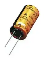


B41858C6227M000
Electrolytic Capacitor, 220 µF, 50 V, ± 20%, Radial Leaded, 5000 hours @ 105°C, Polar
- Manufacturer: TDK
- Product type: Leaded Aluminium Electrolytic Capacitors
- ESR: 1.4ohm
- SVHC: No SVHC (25-Jun-2025)
- Polarity: Polar
- Capacitance: 220µF
- Voltage(DC): 50V
- Lead Spacing: 5mm
- Product Range: B41858 Series
- Product Width: -
- Qualification: AEC-Q200
- Product Height: 16mm
- Product Length: -
- Ripple Current: 778mA
- Product Diameter: 10mm
- Capacitor Terminals: Radial Leaded
- Capacitance Tolerance: ± 20%
- Lifetime @ Temperature: 5000 hours @ 105°C
- Capacitor Case / Package: -
- Operating Temperature Max: 105°C
- Operating Temperature Min: -55°C
| Delivery and price | |
|---|---|
| Units per pack | 1000 |
| Price | 0.221 € |
| Current stock | 1000+ |
| Lead time | 30 days |
## Aluminum electrolytic capacitors, Aluminum electrolytic capacitors – single-ended capacitors **Series/Type: B41858**

The following products presented in this data sheet are being withdrawn.

|Ordering Code|Substitute Product|Date of Withdrawal|Deadline Last<br>Orders|Last Shipments|
|---|---|---|---|---|
|B41858C3337M000||2018-06-22|2018-09-30|2018-12-31|
|B41858C3337M006||2018-06-22|2018-09-30|2018-12-31|
|B41858C3337M008||2023-06-09|2023-11-30|2024-02-29|


|Ordering Code|Substitute Product|Date of Withdrawal|Deadline Last<br>Orders|Last Shipments|
|---|---|---|---|---|
|B41858C3397M000||2023-06-09|2023-11-30|2024-02-29|
|B41858C3397M006||2023-06-09|2023-11-30|2024-02-29|
|B41858C3397M008||2018-06-22|2018-09-30|2018-12-31|
|B41858C3477M000||2023-06-09|2023-11-30|2024-02-29|
|B41858C3477M006||2023-06-09|2023-11-30|2024-02-29|
|B41858C3477M008||2023-06-09|2023-11-30|2024-02-29|
|B41858C6107M000||2023-06-09|2023-11-30|2024-02-29|
|B41858C6107M006||2023-06-09|2023-11-30|2024-02-29|
|B41858C6107M008||2023-06-09|2023-11-30|2024-02-29|
|B41858C7107M000||2023-06-09|2023-11-30|2024-02-29|
|B41858C7107M006||2023-06-09|2023-11-30|2024-02-29|
|B41858C7107M008||2023-06-09|2023-11-30|2024-02-29|
|B41858C7157M000||2023-06-09|2023-11-30|2024-02-29|
|B41858C7157M006||2023-06-09|2023-11-30|2024-02-29|
|B41858C7157M008||2023-06-09|2023-11-30|2024-02-29|
|B41858C9226M000||2023-06-09|2023-11-30|2024-02-29|
|B41858C9226M006||2023-06-09|2023-11-30|2024-02-29|
|B41858C9226M008||2023-06-09|2023-11-30|2024-02-29|
|B41858D4277M000||2023-06-09|2023-11-30|2024-02-29|
|B41858D4277M006||2023-06-09|2023-11-30|2024-02-29|
|B41858D4277M008||2023-06-09|2023-11-30|2024-02-29|
|B41858D4337M000||2023-06-09|2023-11-30|2024-02-29|
|B41858D4337M006||2023-06-09|2023-11-30|2024-02-29|
|B41858D4337M008||2023-06-09|2023-11-30|2024-02-29|
|B41858D5187M000||2023-06-09|2023-11-30|2024-02-29|
|B41858D5187M006||2023-06-09|2023-11-30|2024-02-29|
|B41858D5187M008||2023-06-09|2023-11-30|2024-02-29|
|B41858D5227M000||2023-06-09|2023-11-30|2024-02-29|
|B41858D5227M006||2023-06-09|2023-11-30|2024-02-29|
|B41858D5227M008||2023-06-09|2023-11-30|2024-02-29|
|B41858D7127M000||2023-06-09|2023-11-30|2024-02-29|
|B41858D7127M006||2023-06-09|2023-11-30|2024-02-29|
|B41858D7127M008||2023-06-09|2023-11-30|2024-02-29|
|B41858G8686M000||2023-06-09|2023-11-30|2024-02-29|
|B41858G8686M006||2023-06-09|2023-11-30|2024-02-29|
|B41858G8686M008||2023-06-09|2023-11-30|2024-02-29|


Please contact your nearest TDK sales office if you need support in selecting a suitable substitute. The addresses of our worldwide sales network are presented at www.tdk-electronics.tdk.com/sales.

~~eee~~ **Single-ended capacitors B41858 Low impedance 105** ° **C**

## **Long-life grade capacitors**

## **Applications**

Automotive electronics

## **Features**

Low impedance at high frequency High reliability Low ESR High ripple current capability RoHS-compatible

## **Construction**

Radial leads

Charge-discharge proof, polar Aluminum case with PET insulating sleeve Minus pole marking on the insulating sleeve Case with safety vent

## **Delivery mode**

Terminal configurations and packing:

Bulk

Taped, Ammo pack Cut Kinked PAPR (Protection Against Polarity Reversal): crimped leads, J leads, bent leads

Refer to chapter "Single-ended capacitors Taping, packing and lead configurations" for further details.

Please read _Cautions and warnings_ and _Important notes_ at the end of this document.

Page 2 of 32

**B41858 Low impedance** � **105** ° **C**

**==> picture [61 x 90] intentionally omitted <==**

## **Specifications and characteristics in brief**

|Rated voltage VR<br>Surge voltage VS|10 ... 100 V DC<br>1.15�VR|10 ... 100 V DC<br>1.15�VR|10 ... 100 V DC<br>1.15�VR|10 ... 100 V DC<br>1.15�VR|10 ... 100 V DC<br>1.15�VR|10 ... 100 V DC<br>1.15�VR|10 ... 100 V DC<br>1.15�VR|||
|---|---|---|---|---|---|---|---|---|---|
|Rated capacitance CR<br>Capacitance tolerance|22 ... 10000 μF<br>±20%�M|||||||||
|Dissipation factor tanδ<br>(20°C, 120 Hz)|For capacitance higher than 1000 μF add 0.02 for every<br>1000μF.|||||||increase of||
||VR (V DC)||10|16|25|35|50|63|100|
||tanδ (max.)||0.19|0.16|0.14|0.12|0.10|0.10|0.08|
|Leakage current Ileak<br>(20°C, 5 min)||||||||||
|Self-inductance ESL|Diameter(mm)||8 ... 12.5||16||18|||
||ESL(nH)||20||26||34|||
|Useful life1)<br>105°C; VR; IAC,R|> 3000 h for d = 8 mm<br>> 5000 h for d≥10 mm|||Requirements:<br>�ΔC/C�≤40% of initial value<br>tanδ<br>≤3 times initial specified limit<br>Ileak<br>≤initial specified limit||||||
|Voltage endurance test<br>105°C; VR|3000 h for d = 8 mm<br>5000 h for d≥10 mm|||Post test requirements:<br>�ΔC/C�≤30% of initial value<br>tanδ<br>≤2 times initial specified limit<br>Ileak<br>≤initial specified limit||||||
|Vibration resistance test|To IEC 60068-2-6, test Fc:<br>Frequency range 10 Hz ... 2 kHz, displacement amplitude max. 1.5 mm,<br>acceleration max. 20_g,_duration 3×2 h.<br>Capacitor rigidly clamped by the aluminum case e.g. using our<br>standard fixture|||||||||
|IEC climatic category|To IEC 60068-1:<br>55/105/56(�55°C/+105°C/56 days dampheat test)|||||||||
|Sectional specification|IEC 60384-4|||||||||
|Reference standard|AEC-Q2002)|||||||||


> 1) Refer to chapter "General technical information, 5 Useful life" on how to interpret useful life.

> 2) Refer to chapter "General technical information, 2.3 AEC-Q200 standard" for further details.

Please read _Cautions and warnings_ and _Important notes_ at the end of this document.

Page 3 of 32

**==> picture [61 x 57] intentionally omitted <==**

**B41858 Low impedance** � **105** ° **C**

## **Dimensional drawings**

## **With stand-off rubber seal**

Diameters (mm): 10, 12.5, 16, 18

## **With flat rubber seal**

Diameter (mm): 8

**==> picture [219 x 100] intentionally omitted <==**

**==> picture [146 x 98] intentionally omitted <==**

**==> picture [48 x 34] intentionally omitted <==**

## **Dimensions and weights**

|Dimensions (mm)<br>d +0.5|l|a±0.5|b|Approx. weight<br>g|
|---|---|---|---|---|
|8|11.5 +1.5|3.5|0.60±0.05|1.0|
|10|12.5 +1.0|5.0|0.60±0.05|1.6|
|10|16 +1.0|5.0|0.60±0.05|1.9|
|10|20 +2.0|5.0|0.60±0.05|2.6|
|12.5|20 +2.0|5.0|0.60±0.05|3.6|
|12.5|25 +2.0|5.0|0.60±0.05|4.5|
|16|20 +2.0|7.5|0.80±0.05|5.5|
|16|25 +2.0|7.5|0.80±0.05|7.5|
|16|31.5 +2.0|7.5|0.80±0.05|7.8|
|16|35.5 +2.0|7.5|0.80±0.05|9.2|
|18|20 +2.0|7.5|0.80±0.1|8.0|
|18|25 +2.0|7.5|0.80±0.1|9.0|
|18|31.5 +2.0|7.5|0.80±0.1|11.0|
|18|35 +2.0|7.5|0.80±0.1|13.0|
|18|40 +2.0|7.5|0.80±0.1|16.0|


Please read _Cautions and warnings_ and _Important notes_ at the end of this document.

Page 4 of 32

**B41858 Low impedance** � **105** ° **C**

**==> picture [61 x 90] intentionally omitted <==**

## **Overview of available types**

Other voltage and capacitance ratings are available upon request.

|VR (V DC)|10|16|25|35|
|---|---|---|---|---|
||Case dimensions d|×l(mm)|||
|CR (μF)|||||
|100||||8<br>×11.5|
|120||||8<br>×11.5|
|150||||8<br>×11.5|
|180|||8<br>×11.5|10<br>×12.5|
|220|||8<br>×11.5|10<br>×12.5|
|270||8<br>×11.5|10<br>×12.5||
|330|8<br>×11.5|8<br>×11.5|10<br>×12.5|10<br>×16|
|390|8<br>×11.5||||
|470|8<br>×11.5|10<br>×12.5|10<br>×16|10<br>×20|
|560|10<br>×12.5|10<br>×16|10<br>×16|10<br>×20|
|680|10<br>×12.5|10<br>×16|10<br>×20|12.5×20|
|820|10<br>×16|10<br>×20|10<br>×20||
|1000|10<br>×16|10<br>×20|12.5×20|12.5×25<br>16<br>×20|
|1200|10<br>×16|10<br>×20||16<br>×20|
|1500|10<br>×20|12.5×20|12.5×25|16<br>×25|
|1800|10<br>×20|12.5×25|16<br>×20|16<br>×25<br>18<br>×20|
|2200|12.5×20|12.5×25|16<br>×25<br>18<br>×20|18<br>×25|
|2700|12.5×25|16<br>×20|16<br>×31.5<br>18<br>×20|18<br>×31.5|
|3300|12.5×25<br>16<br>×20|16<br>×25|18<br>×25|16<br>×35.5<br>18<br>×31.5|
|3900|16<br>×20|16<br>×31.5<br>18<br>×20|16<br>×35.5<br>18<br>×31.5|18<br>×35|
|4700|18<br>×20|18<br>×25|18<br>×31.5|18<br>×40|
|5600|||18<br>×35||
|6800|16<br>×31.5|18<br>×31.5|18<br>×40||
|8200|18<br>×31.5|18<br>×35|||
|10000|18<br>×35|18<br>×40|||


Please read _Cautions and warnings_ and _Important notes_ at the end of this document.

Page 5 of 32

**==> picture [61 x 57] intentionally omitted <==**

**B41858 Low impedance** � **105** ° **C**

## **Overview of available types**

Other voltage and capacitance ratings are available upon request.

|VR (V DC)|50|63|100|
|---|---|---|---|
||Case dimensions d×l(mm)|||
|CR (μF)||||
|22|||8<br>×11.5|
|33|||10<br>×16|
|47|||10<br>×20|
|68||8<br>×11.5||
|100|8<br>×11.5|10<br>×12.5|12.5×20|
|120|10<br>×12.5|10<br>×16|12.5×25|
|150|10<br>×12.5|10<br>×16||
|180|10<br>×16|10<br>×20|16<br>×20|
|220|10<br>×16|10<br>×20|16<br>×25|
|270||12.5×20|18<br>×20|
|330|10<br>×20|12.5×20|16<br>×31.5<br>18<br>×25|
|390||12.5×25|18<br>×31.5|
|470|12.5×20|12.5×25<br>16<br>×20|18<br>×35|
|560|12.5×25||18<br>×35|
|680||16<br>×25<br>18<br>×20|18<br>×40|
|820|16<br>×20|16<br>×31.5<br>18<br>×25||
|1000|16<br>×31.5<br>18<br>×20|16<br>×31.5||
|1200|18<br>×20|18<br>×31.5||
|1500|18<br>×25|18<br>×35||
|1800|16<br>×35.5<br>18<br>×31.5|18<br>×40||
|2200|18<br>×35|||
|2700|18<br>×40|||


Please read _Cautions and warnings_ and _Important notes_ at the end of this document.

Page 6 of 32

**B41858 Low impedance** � **105** ° **C**

**==> picture [61 x 90] intentionally omitted <==**

## **Technical data and ordering codes**

|CR<br>120 Hz<br>20°C<br>μF|Case<br>dimensions<br>d×l<br>mm|ESRmax<br>10 kHz<br>�40°C<br>Ω|ESRmax<br>10 kHz<br>20°C<br>Ω|Zmax<br>100 kHz<br>20°C<br>Ω|IAC,R<br>100 kHz<br>105°C<br>mA|Ordering code<br>(composition see<br>below)|
|---|---|---|---|---|---|---|
|VR= 10 V DC|||||||
|330<br>390<br>470<br>560<br>680<br>820<br>1000<br>1200<br>1500<br>1800<br>2200<br>2700<br>3300<br>3300<br>3900<br>4700<br>6800<br>8200<br>10000|8<br>×11.5<br>8<br>×11.5<br>8<br>×11.5<br>10<br>×12.5<br>10<br>×12.5<br>10<br>×16<br>10<br>×16<br>10<br>×16<br>10<br>×20<br>10<br>×20<br>12.5×20<br>12.5×25<br>12.5×25<br>16<br>×20<br>16<br>×20<br>18<br>×20<br>16<br>×31.5<br>18<br>×31.5<br>18<br>×35|2.195<br>2.195<br>2.195<br>1.035<br>1.035<br>0.946<br>0.946<br>0.944<br>0.584<br>0.584<br>0.496<br>0.327<br>0.327<br>0.307<br>0.307<br>0.271<br>0.192<br>0.165<br>0.160|0.274<br>0.274<br>0.274<br>0.129<br>0.129<br>0.118<br>0.118<br>0.118<br>0.073<br>0.073<br>0.062<br>0.041<br>0.041<br>0.038<br>0.038<br>0.034<br>0.024<br>0.021<br>0.020|0.246<br>0.246<br>0.246<br>0.113<br>0.113<br>0.105<br>0.105<br>0.105<br>0.062<br>0.062<br>0.060<br>0.034<br>0.034<br>0.033<br>0.033<br>0.031<br>0.022<br>0.020<br>0.018|436<br>436<br>436<br>746<br>746<br>846<br>846<br>846<br>1202<br>1202<br>1396<br>2028<br>2028<br>2146<br>2146<br>2381<br>3122<br>3539<br>3864|B41858C3337M***<br>B41858C3397M***<br>B41858C3477M***<br>B41858C3567M***<br>B41858C3687M***<br>B41858C3827M***<br>B41858C3108M***<br>B41858C3128M***<br>B41858C3158M***<br>B41858C3188M***<br>B41858C3228M***<br>B41858C3278M***<br>B41858C3338M***<br>B41858D3338M***<br>B41858D3398M***<br>B41858C3478M***<br>B41858C3688M***<br>B41858C3828M***<br>B41858C3109M***|


## **Composition of ordering code**

- *** = Version

   - 000 = for standard leads, bulk

   - 001 = for kinked leads, bulk (for d × l = 10 × 20 mm ... 18 × 40 mm)

   - 002 = for cut leads, bulk (for ∅ 10 ... 18 mm)

   - 003 = for crimped leads, blister (for ∅ 16 ... 18 mm)

   - 004 = for J leads, blister (for ∅ 10 ... 18 mm, excluding d × l = 18 × 40 mm)

   - 006 = for taped leads, Ammo pack, lead spacing F = 3.5 mm (for ∅ 8 mm)

   - 008 = for taped leads, Ammo pack, lead spacing F = 5.0 mm (for ∅ 8 ... 12.5 mm)

   - 009 = for taped leads, Ammo pack, lead spacing F = 7.5 mm (for d × l = 16 × 20 ... 16 × 31.5 mm and 18 × 20 ... 18 × 31.5 mm)

   - 012 = for bent 90° leads, blister (for ∅ 16 ... 18 mm)

Please read _Cautions and warnings_ and _Important notes_ at the end of this document.

Page 7 of 32

**==> picture [61 x 57] intentionally omitted <==**

**B41858 Low impedance** � **105** ° **C**

## **Technical data and ordering codes**

|CR<br>120 Hz<br>20°C<br>μF|Case<br>dimensions<br>d×l<br>mm|ESRmax<br>10 kHz<br>�40°C<br>Ω|ESRmax<br>10 kHz<br>20°C<br>Ω|Zmax<br>100 kHz<br>20°C<br>Ω|IAC,R<br>100 kHz<br>105°C<br>mA|Ordering code<br>(composition see<br>below)|
|---|---|---|---|---|---|---|
|VR= 16 V DC|||||||
|270<br>330<br>470<br>560<br>680<br>820<br>1000<br>1200<br>1500<br>1800<br>2200<br>2700<br>3300<br>3900<br>3900<br>4700<br>6800<br>8200<br>10000|8<br>×11.5<br>8<br>×11.5<br>10<br>×12.5<br>10<br>×16<br>10<br>×16<br>10<br>×20<br>10<br>×20<br>10<br>×20<br>12.5×20<br>12.5×25<br>12.5×25<br>16<br>×20<br>16<br>×25<br>16<br>×31.5<br>18<br>×20<br>18<br>×25<br>18<br>×31.5<br>18<br>×35<br>18<br>×40|2.192<br>2.192<br>1.035<br>0.944<br>0.946<br>0.584<br>0.584<br>0.584<br>0.496<br>0.327<br>0.327<br>0.307<br>0.251<br>0.192<br>0.271<br>0.217<br>0.165<br>0.160<br>0.125|0.274<br>0.274<br>0.129<br>0.118<br>0.118<br>0.073<br>0.073<br>0.073<br>0.062<br>0.041<br>0.041<br>0.038<br>0.031<br>0.024<br>0.034<br>0.027<br>0.021<br>0.020<br>0.016|0.246<br>0.246<br>0.113<br>0.105<br>0.105<br>0.062<br>0.062<br>0.062<br>0.060<br>0.034<br>0.034<br>0.033<br>0.029<br>0.022<br>0.031<br>0.024<br>0.020<br>0.018<br>0.015|436<br>436<br>746<br>846<br>846<br>1202<br>1202<br>1202<br>1396<br>2028<br>2028<br>2146<br>2483<br>3122<br>2381<br>2941<br>3539<br>3864<br>4467|B41858D4277M***<br>B41858D4337M***<br>B41858C4477M***<br>B41858C4567M***<br>B41858C4687M***<br>B41858C4827M***<br>B41858C4108M***<br>B41858C4128M***<br>B41858C4158M***<br>B41858C4188M***<br>B41858C4228M***<br>B41858C4278M***<br>B41858C4338M***<br>B41858D4398M***<br>B41858C4398M***<br>B41858C4478M***<br>B41858C4688M***<br>B41858C4828M***<br>B41858C4109M***|


## **Composition of ordering code**

- *** = Version

   - 000 = for standard leads, bulk

   - 001 = for kinked leads, bulk (for d × l = 10 × 20 mm ... 18 × 40 mm)

   - 002 = for cut leads, bulk (for ∅ 10 ... 18 mm)

   - 003 = for crimped leads, blister (for ∅ 16 ... 18 mm)

   - 004 = for J leads, blister (for ∅ 10 ... 18 mm, excluding d × l = 18 × 40 mm)

   - 006 = for taped leads, Ammo pack, lead spacing F = 3.5 mm (for ∅ 8 mm)

   - 008 = for taped leads, Ammo pack, lead spacing F = 5.0 mm (for ∅ 8 ... 12.5 mm)

   - 009 = for taped leads, Ammo pack, lead spacing F = 7.5 mm (for d × l = 16 × 20 ... 16 × 31.5 mm and 18 × 20 ... 18 × 31.5 mm)

   - 012 = for bent 90° leads, blister (for ∅ 16 ... 18 mm)

Please read _Cautions and warnings_ and _Important notes_ at the end of this document.

Page 8 of 32

**B41858 Low impedance** � **105** ° **C**

**==> picture [61 x 90] intentionally omitted <==**

## **Technical data and ordering codes**

|CR<br>120 Hz<br>20°C<br>μF|Case<br>dimensions<br>d×l<br>mm|ESRmax<br>10 kHz<br>�40°C<br>Ω|ESRmax<br>10 kHz<br>20°C<br>Ω|Zmax<br>100 kHz<br>20°C<br>Ω|IAC,R<br>100 kHz<br>105°C<br>mA|Ordering code<br>(composition see<br>below)|
|---|---|---|---|---|---|---|
|VR= 25 V DC|||||||
|180<br>220<br>270<br>330<br>470<br>560<br>680<br>820<br>1000<br>1500<br>1800<br>2200<br>2200<br>2700<br>2700<br>3300<br>3900<br>3900<br>4700<br>5600<br>6800|8<br>×11.5<br>8<br>×11.5<br>10<br>×12.5<br>10<br>×12.5<br>10<br>×16<br>10<br>×16<br>10<br>×20<br>10<br>×20<br>12.5×20<br>12.5×25<br>16<br>×20<br>16<br>×25<br>18<br>×20<br>16<br>×31.5<br>18<br>×20<br>18<br>×25<br>16<br>×35.5<br>18<br>×31.5<br>18<br>×31.5<br>18<br>×35<br>18<br>×40|2.192<br>2.192<br>1.032<br>1.035<br>0.946<br>0.944<br>0.584<br>0.584<br>0.496<br>0.327<br>0.307<br>0.251<br>0.248<br>0.192<br>0.271<br>0.217<br>0.168<br>0.165<br>0.165<br>0.160<br>0.128|0.274<br>0.274<br>0.129<br>0.129<br>0.118<br>0.118<br>0.073<br>0.073<br>0.062<br>0.041<br>0.038<br>0.031<br>0.031<br>0.024<br>0.034<br>0.027<br>0.021<br>0.021<br>0.021<br>0.020<br>0.016|0.246<br>0.246<br>0.113<br>0.113<br>0.105<br>0.105<br>0.062<br>0.062<br>0.060<br>0.034<br>0.033<br>0.029<br>0.031<br>0.022<br>0.031<br>0.024<br>0.019<br>0.020<br>0.020<br>0.018<br>0.015|436<br>436<br>746<br>746<br>846<br>846<br>1202<br>1202<br>1396<br>2028<br>2146<br>2483<br>2381<br>3122<br>2381<br>2941<br>3408<br>3539<br>3539<br>3864<br>4467|B41858D5187M***<br>B41858D5227M***<br>B41858C5277M***<br>B41858C5337M***<br>B41858C5477M***<br>B41858C5567M***<br>B41858C5687M***<br>B41858C5827M***<br>B41858C5108M***<br>B41858C5158M***<br>B41858C5188M***<br>B41858C5228M***<br>B41858E5228M***<br>B41858D5278M***<br>B41858C5278M***<br>B41858C5338M***<br>B41858D5398M***<br>B41858C5398M***<br>B41858D5478M***<br>B41858D5568M***<br>B41858C5688M***|


## **Composition of ordering code**

- *** = Version

   - 000 = for standard leads, bulk

   - 001 = for kinked leads, bulk (for d × l = 10 × 20 mm ... 18 × 40 mm)

   - 002 = for cut leads, bulk (for ∅ 10 ... 18 mm)

   - 003 = for crimped leads, blister (for ∅ 16 ... 18 mm)

   - 004 = for J leads, blister (for ∅ 10 ... 18 mm, excluding d × l = 18 × 40 mm)

   - 006 = for taped leads, Ammo pack, lead spacing F = 3.5 mm (for ∅ 8 mm)

   - 008 = for taped leads, Ammo pack, lead spacing F = 5.0 mm (for ∅ 8 ... 12.5 mm)

   - 009 = for taped leads, Ammo pack, lead spacing F = 7.5 mm (for d × l = 16 × 20 ... 16 × 31.5 mm and 18 × 20 ... 18 × 31.5 mm)

   - 012 = for bent 90° leads, blister (for ∅ 16 ... 18 mm)

Please read _Cautions and warnings_ and _Important notes_ at the end of this document.

Page 9 of 32

**==> picture [61 x 57] intentionally omitted <==**

**B41858 Low impedance** � **105** ° **C**

## **Technical data and ordering codes**

|CR<br>120 Hz<br>20°C<br>μF|Case<br>dimensions<br>d×l<br>mm|ESRmax<br>10 kHz<br>�40°C<br>Ω|ESRmax<br>10 kHz<br>20°C<br>Ω|Zmax<br>100 kHz<br>20°C<br>Ω|IAC,R<br>100 kHz<br>105°C<br>mA|Ordering code<br>(composition see<br>below)|
|---|---|---|---|---|---|---|
|VR= 35 V DC|||||||
|100<br>120<br>150<br>180<br>220<br>330<br>470<br>560<br>680<br>1000<br>1000<br>1200<br>1500<br>1800<br>1800<br>2200<br>2700<br>3300<br>3300<br>3900<br>4700|8<br>×11.5<br>8<br>×11.5<br>8<br>×11.5<br>10<br>×12.5<br>10<br>×12.5<br>10<br>×16<br>10<br>×20<br>10<br>×20<br>12.5×20<br>12.5×25<br>16<br>×20<br>16<br>×20<br>16<br>×25<br>16<br>×25<br>18<br>×20<br>18<br>×25<br>18<br>×31.5<br>16<br>×35.5<br>18<br>×31.5<br>18<br>×35<br>18<br>×40|2.192<br>2.192<br>2.192<br>1.035<br>1.035<br>0.946<br>0.584<br>0.584<br>0.496<br>0.327<br>0.304<br>0.307<br>0.251<br>0.248<br>0.271<br>0.217<br>0.165<br>0.168<br>0.165<br>0.160<br>0.125|0.274<br>0.274<br>0.274<br>0.129<br>0.129<br>0.118<br>0.073<br>0.073<br>0.062<br>0.041<br>0.038<br>0.038<br>0.031<br>0.031<br>0.034<br>0.027<br>0.021<br>0.021<br>0.021<br>0.020<br>0.016|0.246<br>0.246<br>0.246<br>0.113<br>0.113<br>0.105<br>0.062<br>0.062<br>0.060<br>0.034<br>0.033<br>0.033<br>0.029<br>0.029<br>0.031<br>0.024<br>0.020<br>0.019<br>0.020<br>0.018<br>0.015|436<br>436<br>436<br>746<br>746<br>846<br>1202<br>1202<br>1396<br>2028<br>2146<br>2146<br>2483<br>2483<br>2381<br>2941<br>3539<br>3408<br>3539<br>3864<br>4467|B41858C7107M***<br>B41858D7127M***<br>B41858C7157M***<br>B41858C7187M***<br>B41858C7227M***<br>B41858C7337M***<br>B41858C7477M***<br>B41858C7567M***<br>B41858C7687M***<br>B41858C7108M***<br>B41858D7108M***<br>B41858C7128M***<br>B41858C7158M***<br>B41858E7188M***<br>B41858C7188M***<br>B41858C7228M***<br>B41858C7278M***<br>B41858E7338M***<br>B41858D7338M***<br>B41858C7398M***<br>B41858C7478M***|


## **Composition of ordering code**

- *** = Version

   - 000 = for standard leads, bulk

   - 001 = for kinked leads, bulk (for d × l = 10 × 20 mm ... 18 × 40 mm)

   - 002 = for cut leads, bulk (for ∅ 10 ... 18 mm)

   - 003 = for crimped leads, blister (for ∅ 16 ... 18 mm)

   - 004 = for J leads, blister (for ∅ 10 ... 18 mm, excluding d × l = 18 × 40 mm)

   - 006 = for taped leads, Ammo pack, lead spacing F = 3.5 mm (for ∅ 8 mm)

   - 008 = for taped leads, Ammo pack, lead spacing F = 5.0 mm (for ∅ 8 ... 12.5 mm)

   - 009 = for taped leads, Ammo pack, lead spacing F = 7.5 mm (for d × l = 16 × 20 ... 16 × 31.5 mm and 18 × 20 ... 18 × 31.5 mm)

   - 012 = for bent 90° leads, blister (for ∅ 16 ... 18 mm)

Please read _Cautions and warnings_ and _Important notes_ at the end of this document.

Page 10 of 32

**B41858 Low impedance** � **105** ° **C**

**==> picture [61 x 90] intentionally omitted <==**

## **Technical data and ordering codes**

|CR<br>120 Hz<br>20°C<br>μF|Case<br>dimensions<br>d×l<br>mm|ESRmax<br>10 kHz<br>�40°C<br>Ω|ESRmax<br>10 kHz<br>20°C<br>Ω|Zmax<br>100 kHz<br>20°C<br>Ω|IAC,R<br>100 kHz<br>105°C<br>mA|Ordering code<br>(composition see<br>below)|
|---|---|---|---|---|---|---|
|VR= 50 V DC|||||||
|100<br>120<br>150<br>180<br>220<br>330<br>470<br>560<br>820<br>1000<br>1000<br>1200<br>1500<br>1800<br>1800<br>2200<br>2700|8<br>×11.5<br>10<br>×12.5<br>10<br>×12.5<br>10<br>×16<br>10<br>×16<br>10<br>×20<br>12.5×20<br>12.5×25<br>16<br>×20<br>16<br>×31.5<br>18<br>×20<br>18<br>×20<br>18<br>×25<br>16<br>×35.5<br>18<br>×31.5<br>18<br>×35<br>18<br>×40|5.168<br>2.984<br>2.984<br>1.400<br>1.400<br>1.000<br>0.880<br>0.712<br>0.401<br>0.260<br>0.477<br>0.384<br>0.382<br>0.232<br>0.300<br>0.268<br>0.210|0.646<br>0.373<br>0.373<br>0.175<br>0.175<br>0.125<br>0.110<br>0.089<br>0.050<br>0.032<br>0.048<br>0.048<br>0.038<br>0.029<br>0.030<br>0.027<br>0.021|0.573<br>0.336<br>0.336<br>0.160<br>0.160<br>0.118<br>0.104<br>0.082<br>0.046<br>0.030<br>0.044<br>0.044<br>0.036<br>0.026<br>0.028<br>0.024<br>0.020|340<br>555<br>555<br>778<br>778<br>1030<br>1300<br>1490<br>1820<br>2653<br>1997<br>1997<br>2417<br>2896<br>2989<br>3320<br>3871|B41858C6107M***<br>B41858C6127M***<br>B41858C6157M***<br>B41858C6187M***<br>B41858C6227M***<br>B41858C6337M***<br>B41858C6477M***<br>B41858C6567M***<br>B41858D6827M***<br>B41858C6108M***<br>B41858D6108M***<br>B41858C6128M***<br>B41858C6158M***<br>B41858D6188M***<br>B41858C6188M***<br>B41858C6228M***<br>B41858C6278M***|


## **Composition of ordering code**

- *** = Version

   - 000 = for standard leads, bulk

   - 001 = for kinked leads, bulk (for d × l = 10 × 20 mm ... 18 × 40 mm)

   - 002 = for cut leads, bulk (for ∅ 10 ... 18 mm)

   - 003 = for crimped leads, blister (for ∅ 16 ... 18 mm)

   - 004 = for J leads, blister (for ∅ 10 ... 18 mm, excluding d × l = 18 × 40 mm)

   - 006 = for taped leads, Ammo pack, lead spacing F = 3.5 mm (for ∅ 8 mm)

   - 008 = for taped leads, Ammo pack, lead spacing F = 5.0 mm (for ∅ 8 ... 12.5 mm)

   - 009 = for taped leads, Ammo pack, lead spacing F = 7.5 mm (for d × l = 16 × 20 ... 16 × 31.5 mm and 18 × 20 ... 18 × 31.5 mm)

   - 012 = for bent 90° leads, blister (for ∅ 16 ... 18 mm)

Please read _Cautions and warnings_ and _Important notes_ at the end of this document.

Page 11 of 32

**==> picture [61 x 57] intentionally omitted <==**

**B41858 Low impedance** � **105** ° **C**

## **Technical data and ordering codes**

|CR<br>120 Hz<br>20°C<br>μF|Case<br>dimensions<br>d×l<br>mm|ESRmax<br>10 kHz<br>�40°C<br>Ω|ESRmax<br>10 kHz<br>20°C<br>Ω|Zmax<br>100 kHz<br>20°C<br>Ω|IAC,R<br>100 kHz<br>105°C<br>mA|Ordering code<br>(composition see<br>below)|
|---|---|---|---|---|---|---|
|VR= 63 V DC|||||||
|68<br>100<br>120<br>150<br>180<br>220<br>270<br>330<br>390<br>470<br>470<br>680<br>680<br>820<br>820<br>1000<br>1200<br>1500<br>1800|8<br>×11.5<br>10<br>×12.5<br>10<br>×16<br>10<br>×16<br>10<br>×20<br>10<br>×20<br>12.5×20<br>12.5×20<br>12.5×25<br>12.5×25<br>16<br>×20<br>16<br>×25<br>18<br>×20<br>16<br>×31.5<br>18<br>×25<br>16<br>×31.5<br>18<br>×31.5<br>18<br>×35<br>18<br>×40|4.328<br>4.616<br>3.075<br>2.464<br>1.986<br>1.592<br>1.688<br>1.688<br>1.236<br>0.992<br>1.037<br>0.772<br>0.960<br>0.541<br>0.761<br>0.540<br>0.518<br>0.441<br>0.375|0.541<br>0.577<br>0.308<br>0.308<br>0.199<br>0.199<br>0.169<br>0.169<br>0.124<br>0.124<br>0.104<br>0.077<br>0.096<br>0.054<br>0.076<br>0.054<br>0.052<br>0.044<br>0.038|0.488<br>0.500<br>0.279<br>0.279<br>0.180<br>0.180<br>0.153<br>0.153<br>0.112<br>0.112<br>0.094<br>0.070<br>0.087<br>0.049<br>0.069<br>0.049<br>0.047<br>0.040<br>0.034|310<br>354<br>519<br>519<br>705<br>705<br>876<br>876<br>1118<br>1118<br>1272<br>1600<br>1427<br>2092<br>1735<br>2092<br>2294<br>2592<br>2967|B41858G8686M***<br>B41858G8107M***<br>B41858G8127M***<br>B41858G8157M***<br>B41858G8187M***<br>B41858G8227M***<br>B41858G8277M***<br>B41858G8337M***<br>B41858G8397M***<br>B41858G8477M***<br>B41858H8477M***<br>B41858G8687M***<br>B41858H8687M***<br>B41858G8827M***<br>B41858H8827M***<br>B41858G8108M***<br>B41858G8128M***<br>B41858G8158M***<br>B41858G8188M***|


## **Composition of ordering code**

- *** = Version

   - 000 = for standard leads, bulk

   - 001 = for kinked leads, bulk (for d × l = 10 × 20 mm ... 18 × 40 mm)

   - 002 = for cut leads, bulk (for ∅ 10 ... 18 mm)

   - 003 = for crimped leads, blister (for ∅ 16 ... 18 mm)

   - 004 = for J leads, blister (for ∅ 10 ... 18 mm, excluding d × l = 18 × 40 mm)

   - 006 = for taped leads, Ammo pack, lead spacing F = 3.5 mm (for ∅ 8 mm)

   - 008 = for taped leads, Ammo pack, lead spacing F = 5.0 mm (for ∅ 8 ... 12.5 mm)

   - 009 = for taped leads, Ammo pack, lead spacing F = 7.5 mm (for d × l = 16 × 20 ... 16 × 31.5 mm and 18 × 20 ... 18 × 31.5 mm)

   - 012 = for bent 90° leads, blister (for ∅ 16 ... 18 mm)

Please read _Cautions and warnings_ and _Important notes_ at the end of this document.

Page 12 of 32

**B41858**

**Low impedance** � **105** ° **C**

**==> picture [61 x 90] intentionally omitted <==**

## **Technical data and ordering codes**

|CR<br>120 Hz<br>20°C<br>μF|Case<br>dimensions<br>d×l<br>mm|ESRmax<br>10 kHz<br>�40°C<br>Ω|ESRmax<br>10 kHz<br>20°C<br>Ω|Zmax<br>100 kHz<br>20°C<br>Ω|IAC,R<br>100 kHz<br>105°C<br>mA|Ordering code<br>(composition see<br>below)|
|---|---|---|---|---|---|---|
|VR= 100 V DC|||||||
|22<br>33<br>47<br>100<br>120<br>180<br>220<br>270<br>330<br>330<br>390<br>470<br>560<br>680|8<br>×11.5<br>10<br>×16<br>10<br>×20<br>12.5×20<br>12.5×25<br>16<br>×20<br>16<br>×25<br>18<br>×20<br>16<br>×31.5<br>18<br>×25<br>18<br>×31.5<br>18<br>×35<br>18<br>×35<br>18<br>×40|12.219<br>6.542<br>3.688<br>3.048<br>2.038<br>1.313<br>0.985<br>1.260<br>0.973<br>1.008<br>0.720<br>0.679<br>0.679<br>0.438|1.222<br>0.654<br>0.461<br>0.305<br>0.204<br>0.131<br>0.099<br>0.126<br>0.097<br>0.101<br>0.072<br>0.068<br>0.068<br>0.044|1.114<br>0.589<br>0.423<br>0.281<br>0.188<br>0.122<br>0.091<br>0.119<br>0.090<br>0.095<br>0.068<br>0.063<br>0.063<br>0.042|205<br>357<br>460<br>647<br>864<br>1119<br>1402<br>1220<br>1546<br>1477<br>1907<br>2061<br>2061<br>2683|B41858C9226M***<br>B41858C9336M***<br>B41858C9476M***<br>B41858C9107M***<br>B41858C9127M***<br>B41858D9187M***<br>B41858C9227M***<br>B41858D9277M***<br>B41858C9337M***<br>B41858D9337M***<br>B41858C9397M***<br>B41858C9477M***<br>B41858C9567M***<br>B41858C9687M***|


## **Composition of ordering code**

- *** = Version

   - 000 = for standard leads, bulk

   - 001 = for kinked leads, bulk (for d × l = 10 × 20 mm ... 18 × 40 mm)

   - 002 = for cut leads, bulk (for ∅ 10 ... 18 mm)

   - 003 = for crimped leads, blister (for ∅ 16 ... 18 mm)

   - 004 = for J leads, blister (for ∅ 10 ... 18 mm, excluding d × l = 18 × 40 mm)

   - 006 = for taped leads, Ammo pack, lead spacing F = 3.5 mm (for ∅ 8 mm)

   - 008 = for taped leads, Ammo pack, lead spacing F = 5.0 mm (for ∅ 8 ... 12.5 mm)

   - 009 = for taped leads, Ammo pack, lead spacing F = 7.5 mm (for d × l = 16 × 20 ... 16 × 31.5 mm and 18 × 20 ... 18 × 31.5 mm)

   - 012 = for bent 90° leads, blister (for ∅ 16 ... 18 mm)

Please read _Cautions and warnings_ and _Important notes_ at the end of this document.

Page 13 of 32

**==> picture [61 x 57] intentionally omitted <==**

**B41858 Low impedance** � **105** ° **C**

## **Useful life**[1)]

depending on ambient temperature TA under ripple current operating conditions d = 8 mm

**==> picture [55 x 51] intentionally omitted <==**

**==> picture [52 x 58] intentionally omitted <==**

## **Useful life**[1)]

depending on ambient temperature TA under ripple current operating conditions d ≥ 10 mm

**==> picture [64 x 63] intentionally omitted <==**

1) Refer to chapter "General technical information, 5 Useful life" on how to interpret useful life.

Please read _Cautions and warnings_ and _Important notes_ at the end of this document.

Page 14 of 32

**B41858**

**Low impedance** � **105** ° **C**

**==> picture [61 x 90] intentionally omitted <==**

## **Frequency factor of permissible ripple current IAC versus frequency f**

**==> picture [42 x 46] intentionally omitted <==**

Please read _Cautions and warnings_ and _Important notes_ at the end of this document.

Page 15 of 32

**==> picture [61 x 57] intentionally omitted <==**

**B41858 Low impedance** � **105** ° **C**

## **Taping**

Single-ended capacitors are available taped in Ammo pack from diameter 8 to 18 mm as follows:

Lead spacing F = 3.5 mm (∅ d = 8 mm)

Lead spacing F = 5.0 mm (∅ d **=** 8 … 12.5 mm) Lead spacing F = 7.5 mm (∅ d = 16 ... 18 mm).

The dimensions for F, P1 and 1 max. are specified with reference to the center of the terminal wires.

## **Lead spacing 3.5 mm (** ∅ **d = 8 mm)**

Last 3 digits of ordering code: 006

**==> picture [41 x 45] intentionally omitted <==**

**==> picture [151 x 60] intentionally omitted <==**

**==> picture [61 x 122] intentionally omitted <==**

## **Dimensions in mm**

|∅d|F|H|W|W0|W1|W2|P|P0|P1|I1|t|Δh|D0|
|---|---|---|---|---|---|---|---|---|---|---|---|---|---|
|8|3.5|18.5|18.0|9.5|9.0|3.0|12.|7<br>12.7|4.6|1.0|0.7|1.0|4.0|
|Toler-<br>ance|+0.8<br>�0.2|±1.0|±0.5|min.|±0.5|max.|±1.|0<br>±0.3|±0.6|max.|±0.2|max.|±0.2|


Leads can also run straight through the taping area.

Please read _Cautions and warnings_ and _Important notes_ at the end of this document.

Page 16 of 32

**B41858 Low impedance** � **105** ° **C**

**==> picture [61 x 90] intentionally omitted <==**

## **Lead spacing 5.0 mm (** ∅ **d = 8 mm)**

Last 3 digits of ordering code: 008

**==> picture [55 x 42] intentionally omitted <==**

**==> picture [51 x 55] intentionally omitted <==**

**==> picture [67 x 118] intentionally omitted <==**

**Lead spacing 5.0 mm (** ∅ **d = 10 ... 12.5 mm)**

Last 3 digits of ordering code: 008

**==> picture [56 x 43] intentionally omitted <==**

**==> picture [50 x 54] intentionally omitted <==**

**==> picture [67 x 119] intentionally omitted <==**

## **Dimensions in mm**

|∅d|F|H|W|W0|W1|W2|H0<br>|P|P0|P1|I1|t|Δh|D0|
|---|---|---|---|---|---|---|---|---|---|---|---|---|---|---|
|8|5.0|20.|0<br>0<br>18.0<br>0|9.5|9.0<br>|1.5|16.0<br>|12.7|12.7|3.85|1.0|0.6|1.0|4.0|
|10||19.||9.5|||�<br>|12.7|12.7|3.85|||||
|12.5||19.||11.5|||�<br>|15.0|15.0|5.0|||||
|Toler-<br>ance|+0.8<br>�0.2|±0.|75<br>±0.5|min.|±0.5|max.|±0.5<br>|±1.0|±0.2|±0.5|max.|+0.3<br>�0.2|max.|±0.2|


Taping is available up to dimensions d × l = 12.5 × 25 mm.

Please read _Cautions and warnings_ and _Important notes_ at the end of this document.

Page 17 of 32

**B41858 Low impedance** � **105** ° **C**

**==> picture [61 x 57] intentionally omitted <==**

## **Lead spacing 7.5 mm (** ∅ **d = 16 ...18 mm)**

Last 3 digits of ordering code: 009

**==> picture [81 x 36] intentionally omitted <==**

**==> picture [48 x 55] intentionally omitted <==**

**==> picture [46 x 68] intentionally omitted <==**

## **Dimensions in mm**

|∅d|F|H|W|W0<br>W|1|W2|P|P0|P1|I1|t|ΔP|Δh|D0|
|---|---|---|---|---|---|---|---|---|---|---|---|---|---|---|
|16|7.5|18.5|18.0|12.5<br>9.|0|1.5|30.0|15.0|3.75|1.0|0.7|0|0|4.0|
|18|||||||||||||||
|Toler-<br>ance|±0.8|�0.5<br>+0.75|±0.5|min.<br>±|0.5|max.|±1.0|±0.2|±0.5|max.|±0.2|±1.0|±1.0|±0.2|


Taping is available up to dimensions d × l = 16 × 31.5 mm and 18 × 31.5 mm.

Please read _Cautions and warnings_ and _Important notes_ at the end of this document.

Page 18 of 32

**B41858 Low impedance** � **105** ° **C**

**==> picture [61 x 90] intentionally omitted <==**

## **Cut or kinked leads**

Single-ended capacitors are available with cut or kinked leads. Other lead configurations also available upon request.

## **Cut leads**

Last 3 digits of ordering code: 002

## **With stand-off rubber seal**

**==> picture [154 x 77] intentionally omitted <==**

## **With flat rubber seal**

**==> picture [162 x 79] intentionally omitted <==**

|Case size<br>d×l(mm)|Dimensions (mm)<br>a±0.5|
|---|---|
|10×12.5|5.0|
|10×16|5.0|
|10×20|5.0|
|12.5×20|5.0|
|12.5×25|5.0|
|16×20|7.5|
|16×25|7.5|
|16×31.5|7.5|
|16×35.5|7.5|
|16×40|7.5|
|18×20|7.5|
|18×25|7.5|
|18×31.5|7.5|
|18×35|7.5|
|18×40|7.5|


Please read _Cautions and warnings_ and _Important notes_ at the end of this document.

Page 19 of 32

**==> picture [61 x 57] intentionally omitted <==**

**B41858 Low impedance** � **105** ° **C**

## **Kinked leads**

Last 3 digits of ordering code: 001

## **With stand-off rubber seal**

**==> picture [87 x 46] intentionally omitted <==**

**==> picture [138 x 64] intentionally omitted <==**

## **With flat rubber seal**

|Case size<br>d×l(mm)|Dimensions (mm)<br>a±0.5|
|---|---|
|10×20|5.0|
|12.5×20|5.0|
|12.5×25|5.0|
|16×20|7.5|
|16×25|7.5|
|16×31.5|7.5|
|16×35.5|7.5|
|18×20|7.5|
|18×25|7.5|
|18×31.5|7.5|
|18×35|7.5|
|18×40|7.5|


**==> picture [88 x 45] intentionally omitted <==**

**==> picture [145 x 64] intentionally omitted <==**

Please read _Cautions and warnings_ and _Important notes_ at the end of this document.

Page 20 of 32

**B41858 Low impedance** � **105** ° **C**

**==> picture [61 x 90] intentionally omitted <==**

## **PAPR leads** (Protection Against Polarity Reversal)

These lead configurations ensure correct placement of the capacitor on the PCB with regard to polarity. PAPR leads are available for diameters from 10 mm up to 18 mm. There are three configurations available: Crimped leads, J leads, bent 90° leads.

## **Crimped leads**

Last 3 digits of ordering code: 003

## **With stand-off rubber seal**

**==> picture [243 x 122] intentionally omitted <==**

The series B41897 and B41898 have no sleeve nor minus pole marking, the positive pole is marked on the aluminum case side instead.

## **Suggestion for PCB hole diameter**

**==> picture [48 x 53] intentionally omitted <==**

**==> picture [152 x 95] intentionally omitted <==**

|Case size<br>d×l(mm)|Dimensions (mm)<br>B±0.2<br>C±0.5|Dimensions (mm)<br>B±0.2<br>C±0.5|D±0.1|E±0.1|a±0.5|∅b|
|---|---|---|---|---|---|---|
|16×20|1.5|3.0|1.3|0.3|7.5|0.8±0.05|
|16×25|1.5|3.0|1.3|0.3|7.5|0.8±0.05|
|16×31.5|1.5|3.0|1.3|0.3|7.5|0.8±0.05|
|16×35.5|1.5|3.0|1.3|0.3|7.5|0.8±0.05|
|18×20|1.5|3.0|1.3|0.3|7.5|0.8±0.1|
|18×25|1.5|3.0|1.3|0.3|7.5|0.8±0.1|
|18×31.5|1.5|3.0|1.3|0.3|7.5|0.8±0.1|
|18×35|1.5|3.0|1.3|0.3|7.5|0.8±0.1|
|18×40|1.5|3.0|1.3|0.3|7.5|0.8±0.1|


Please read _Cautions and warnings_ and _Important notes_ at the end of this document.

Page 21 of 32

**==> picture [61 x 57] intentionally omitted <==**

**B41858 Low impedance** � **105** ° **C**

## **J leads**

Last 3 digits of ordering code: 004

**==> picture [177 x 87] intentionally omitted <==**

**==> picture [119 x 117] intentionally omitted <==**

The series B41897 and B41898 have no sleeve nor minus pole marking, the positive pole is marked on the aluminum case side instead.

## **Suggestion for PCB hole diameter**

**==> picture [152 x 97] intentionally omitted <==**

**==> picture [152 x 95] intentionally omitted <==**

|Case size<br>d×l(mm)|Dimensions (mm)<br>C±0.5<br>E±0.5|Dimensions (mm)<br>C±0.5<br>E±0.5|J±0.2|a±0.5|∅b|
|---|---|---|---|---|---|
|10×12.5|3.2|0.7|1.2|5.0|0.6±0.05|
|10×16|3.2|0.7|1.2|5.0|0.6±0.05|
|10×20|3.2|0.7|1.2|5.0|0.6±0.05|
|12.5×20|3.2|0.7|1.2|5.0|0.6±0.05|
|12.5×25|3.2|0.7|1.2|5.0|0.6±0.05|
|16×20|3.5|0.7|1.6|7.5|0.8±0.05|
|16×25|3.5|0.7|1.6|7.5|0.8±0.05|
|16×31.5|3.5|0.7|1.6|7.5|0.8±0.05|
|16×35.5|3.5|0.7|1.6|7.5|0.8±0.05|
|16×40|3.5|0.7|1.6|7.5|0.8±0.05|
|18×20|3.5|0.7|1.6|7.5|0.8±0.1|
|18×25|3.5|0.7|1.6|7.5|0.8±0.1|
|18×31.5|3.5|0.7|1.6|7.5|0.8±0.1|
|18×35|3.5|0.7|1.6|7.5|0.8±0.1|


Please read _Cautions and warnings_ and _Important notes_ at the end of this document.

Page 22 of 32

**B41858 Low impedance** � **105** ° **C**

**==> picture [61 x 90] intentionally omitted <==**

## **Bent 90** ° **leads for horizontal mounting pinning**

Last 3 digits of ordering code: 012

**==> picture [130 x 84] intentionally omitted <==**

**==> picture [126 x 124] intentionally omitted <==**

The series B41897 and B41898 have no sleeve nor minus pole marking, the positive pole is marked on the aluminum case side instead.

|Case size<br>d×l(mm)|Dimensions (mm)<br>C±0.5<br>E±0.5|Dimensions (mm)<br>C±0.5<br>E±0.5|F±0.5|a±0.5|∅b|
|---|---|---|---|---|---|
|16×20|4.0|4.0|12.0|7.5|0.8±0.05|
|16×25|4.0|4.0|12.0|7.5|0.8±0.05|
|16×31.5|4.0|4.0|12.0|7.5|0.8±0.05|
|16×35.5|4.0|4.0|12.0|7.5|0.8±0.05|
|16×40|4.0|4.0|13.0|7.5|0.8±0.05|
|18×20|4.0|4.0|13.0|7.5|0.8±0.1|
|18×25|4.0|4.0|13.0|7.5|0.8±0.1|
|18×31.5|4.0|4.0|13.0|7.5|0.8±0.1|
|18×35|4.0|4.0|13.0|7.5|0.8±0.1|
|18×40|4.0|4.0|13.0|7.5|0.8±0.1|


Bent leads for diameter 12.5 mm available upon request.

Please read _Cautions and warnings_ and _Important notes_ at the end of this document.

Page 23 of 32

**==> picture [61 x 57] intentionally omitted <==**

**B41858 Low impedance** � **105** ° **C**

## **Packing units and box dimensions**

## **Ammo pack**

|Case size<br>d×l<br>mm|Dimensions (mm)<br>Amax<br>Bmax<br>Cmax|Dimensions (mm)<br>Amax<br>Bmax<br>Cmax|Dimensions (mm)<br>Amax<br>Bmax<br>Cmax|Packing<br>units<br>pcs.|
|---|---|---|---|---|
|8×11.5|345|60|240|1000|
|10×12.5|345|60|280|750|
|10×16|345|65|200|500|
|10×20|345|65|200|500|
|12.5×20|345|65|260|500|
|12.5×25|345|70|260|500|
|16×20|325|65|285|300|
|16×25|325|65|285|300|
|16×31.5|325|80|275|300|
|18×20|325|65|285|250|
|18×25|325|65|285|250|
|18×31.5|325|80|275|250|


Please read _Cautions and warnings_ and _Important notes_ at the end of this document.

Page 24 of 32

**B41858 Low impedance** � **105** ° **C**

**==> picture [61 x 90] intentionally omitted <==**

## **Overview of packing units and code numbers**

|||||||||**PAPR**|**PAPR**|
|---|---|---|---|---|---|---|---|---|---|
|Case size<br>d×l<br>mm|Stan-<br>dard,<br>bulk<br>pcs.|Taped,<br>Ammo pack<br>pcs.|||Kinked<br>leads,<br>bulk<br>pcs.|Cut<br>leads,<br>bulk<br>pcs.|Crimped<br>leads,<br>blister<br>pcs.|J leads,<br>blister<br>pcs.|Bent 90°<br>leads,<br>blister<br>pcs.|
|8×11.5|1000|1000|||�|�|�|�||
|10×12.5|1000|750|||�|1000|�|900||
|10×16|1000|500|||�|1000|�|675||
|10×20|500|500|||500|500|�|500||
|12.5×20|350|500|||350|350|�|300|1)|
|12.5×25|250|500|||500|500|�|225|1)|
|16×20|250|300|||200|200|200|200|420|
|16×25|250|300|||200|200|216|216|216|
|16×31.5|200|300|||250|250|180|180|180|
|16×35.5|100|�|||100|100|150|150|150|
|16×40|125|�|||100|100|72|72|72|
|18×20|175|250|||175|175|200|200|420|
|18×25|150|250|||150|150|200|200|200|
|18×31.5|100|250|||100|100|150|150|150|
|18×35|100|�|||100|100|150|150|150|
|18×40|125|�|||100|100|72|�|72|
|The last three<br>digits of the<br>complete<br>ordering code<br>state the lead<br>configuration|**000**|Code|F(mm)|d(mm)|**001**|**002**|**003**|**004**|**012**|
|||**006**<br>**008**<br>**009**|3.5<br>5<br>7.5|8<br>8...12.5<br>16...18||||||


1) Available upon request

Please read _Cautions and warnings_ and _Important notes_ at the end of this document.

Page 25 of 32

**==> picture [61 x 57] intentionally omitted <==**

**B41858 Low impedance** � **105** ° **C**

## **Cautions and warnings**

## **Personal safety**

The electrolytes used have been optimized both with a view to the intended application and with regard to health and environmental compatibility. They do not contain any solvents that are detrimental to health, e.g. dimethyl formamide (DMF) or dimethyl acetamide (DMAC). Furthermore, some of the high-voltage electrolytes used are self-extinguishing.

As far as possible, we do not use any dangerous chemicals or compounds to produce operating electrolytes, although in exceptional cases, such materials must be used in order to achieve specific physical and electrical properties because no alternative materials are currently known. We do, however, restrict the amount of dangerous materials used in our products to an absolute minimum.

Materials and chemicals used in our aluminum electrolytic capacitors are continuously adapted in compliance with the TDK Electronics Corporate Environmental Policy and the latest EU regulations and guidelines such as RoHS, REACH/SVHC, GADSL, and ELV.

MDS (Material Data Sheets) are available on our website for all types listed in the data book. MDS for customer specific capacitors are available upon request. MSDS (Material Safety Data Sheets) are available for our electrolytes upon request.

Nevertheless, the following rules should be observed when handling aluminum electrolytic capacitors: No electrolyte should come into contact with eyes or skin. If electrolyte does come into contact with the skin, wash the affected areas immediately with running water. If the eyes are affected, rinse them for 10 minutes with plenty of water. If symptoms persist, seek medical treatment. Avoid inhaling electrolyte vapor or mists. Workplaces and other affected areas should be well ventilated. Clothing that has been contaminated by electrolyte must be changed and rinsed in water.

Please read _Cautions and warnings_ and _Important notes_ at the end of this document.

Page 26 of 32

**B41858 Low impedance** � **105** ° **C**

**==> picture [61 x 90] intentionally omitted <==**

## **Product safety**

The table below summarizes the safety instructions that must be observed without fail. A detailed description can be found in the relevant sections of seperate file chapter "General technical information".

|Topic|Safety information|Reference<br>chapter "General<br>technical information"|
|---|---|---|
|Polarity|Make sure that polar capacitors are connected<br>with the right polarity.|1<br>"Basic construction of<br>aluminum electrolytic<br>capacitors"|
|Reverse voltage|Voltages of opposite polarity should be prevented<br>byconnectinga diode.|3.1.6<br>"Reverse voltage"|
|Mounting<br>position of screw-<br>terminal capacitors|Screw terminal capacitors must not be mounted<br>with terminals facing down unless otherwise<br>specified.|11.1.<br>"Mounting positions of<br>capacitors with screw<br>terminals"|
|Robustness of<br>terminals|The following maximum tightening torques must<br>not be exceeded when connecting screw<br>terminals:<br>M5: 2.5 Nm<br>M6: 4.0 Nm|11.3<br>"Mounting torques"|
|Mounting of<br>single-ended<br>capacitors|The internal structure of single-ended capacitors<br>might be damaged if excessive force is applied to<br>the lead wires.<br>Avoid any compressive, tensile or flexural stress.<br>Do not move the capacitor after soldering to PC<br>board.<br>Do not pick up the PC board by the soldered<br>capacitor.<br>Do not insert the capacitor on the PC board with a<br>hole space different to the lead space specified.|11.4<br>"Mounting<br>considerations for<br>single-ended capacitors"|
|Soldering|Do not exceed the specified time or temperature<br>limits duringsoldering.|11.5<br>"Soldering"|
|Soldering,<br>cleaningagents|Do not allow halogenated hydrocarbons to come<br>into contact with aluminum electrolytic capacitors.|11.6<br>"Cleaningagents"|
|Upper category<br>temperature|Do not exceed the upper category temperature.|7.2<br>"Maximum permissible<br>operatingtemperature"|
|Passive<br>flammability|Avoid external energy, e.g. fire.|8.1<br>"Passive flammability"|


Please read _Cautions and warnings_ and _Important notes_ at the end of this document.

Page 27 of 32

**==> picture [61 x 57] intentionally omitted <==**

**B41858 Low impedance** � **105** ° **C**

|Topic|Safety information|Reference<br>chapter "General<br>technical information"|
|---|---|---|
|Active<br>flammability|Avoid overload of the capacitors.|8.2<br>"Active flammability"|
|Maintenance|Make periodic inspections of the capacitors.<br>Before the inspection, make sure that the power<br>supply is turned off and carefully discharge the<br>capacitors.<br>Do not apply excessive mechanical stress to the<br>capacitor terminals when mounting.|10<br>"Maintenance"|
|Storage|Do not store capacitors at high temperatures or<br>high humidity. Capacitors should be stored at<br>+5 to +35°C and a relative humidityof≤75%.|7.3<br>"Shelf life and storage<br>conditions"|
|||Reference<br>chapter "Capacitors with<br>screw terminals"|
|Breakdown strength<br>of insulating<br>sleeves|Do not damage the insulating sleeve, especially<br>when ring clips are used for mounting.|"Screw terminals�<br>accessories"|


## **Display of ordering codes for TDK Electronics products**

The ordering code for one and the same product can be represented differently in data sheets, data books, other publications, on the company website, or in order-related documents such as shipping notes, order confirmations and product labels. The varying representations of the ordering codes are due to different processes employed and do not affect the specifications of the respective products.

Detailed information can be found on the Internet under www.tdk-electronics.tdk.com/orderingcodes.

Please read _Cautions and warnings_ and _Important notes_ at the end of this document.

Page 28 of 32

## **B41858 Low impedance** � **105** ° **C**

**==> picture [61 x 90] intentionally omitted <==**

## **Symbols and terms**

|Symbol|English|German|
|---|---|---|
|C<br>CR<br>CS<br>CS,T<br>Cf<br>d<br>dmax<br>ESL<br>ESR<br>ESRf<br>ESRT<br>f<br>I<br>IAC<br>IAC,RMS<br>IAC,f<br>IAC,max<br>IAC,R<br>Ileak<br>Ileak,op<br>l<br>lmax<br>R<br>Rins<br>Rsymm<br>T<br>ΔT<br>TA<br>TC<br>TB<br>t<br>Δt<br>tb|Capacitance<br>Rated capacitance<br>Series capacitance<br>Series capacitance at temperature T<br>Capacitance at frequency f<br>Case diameter, nominal dimension<br>Maximum case diameter<br>Self-inductance<br>Equivalent series resistance<br>Equivalent series resistance at<br>frequency f<br>Equivalent series resistance at<br>temperature T<br>Frequency<br>Current<br>Alternating current (ripple current)<br>Root-mean-square value of alternating<br>current<br>Ripple current at frequency f<br>Maximum permissible ripple current<br>Rated ripple current<br>Leakage current<br>Operating leakage current<br>Case length, nominal dimension<br>Maximum case length (without<br>terminals and mounting stud)<br>Resistance<br>Insulation resistance<br>Balancing resistance<br>Temperature<br>Temperature difference<br>Ambient temperature<br>Case temperature<br>Capacitor base temperature<br>Time<br>Period<br>Service life(operatinghours)|Kapazität<br>Nennkapazität<br>Serienkapazität<br>Serienkapazität bei Temperatur T<br>Kapazität bei Frequenz f<br>Gehäusedurchmesser, Nennmaß<br>Maximaler Gehäusedurchmesser<br>Eigeninduktivität<br>Ersatzserienwiderstand<br>Ersatzserienwiderstand bei Frequenz f<br>Ersatzserienwiderstand bei Temperatur T<br>Frequenz<br>Strom<br>Wechselstrom<br>Wechselstrom, Effektivwert<br>Wechselstrom bei Frequenz f<br>Maximal zulässiger Wechselstrom<br>Nennwechselstrom<br>Reststrom<br>Betriebsreststrom<br>Gehäuselänge, Nennmaß<br>Maximale Gehäuselänge (ohne Anschlüsse<br>und Gewindebolzen)<br>Widerstand<br>Isolationswiderstand<br>Symmetrierwiderstand<br>Temperatur<br>Temperaturdifferenz<br>Umgebungstemperatur<br>Gehäusetemperatur<br>Temperatur des Gehäusebodens<br>Zeit<br>Zeitraum<br>Brauchbarkeitsdauer(Betriebszeit)|


Please read _Cautions and warnings_ and _Important notes_ at the end of this document.

Page 29 of 32

**==> picture [61 x 57] intentionally omitted <==**

**B41858 Low impedance** � **105** ° **C**

|Symbol|English|German|
|---|---|---|
|V<br>VF<br>Vop<br>VR<br>VS<br>XC<br>XL<br>Z<br>ZT<br>tanδ<br>λ<br>ε0<br>εr<br>ω|Voltage<br>Forming voltage<br>Operating voltage<br>Rated voltage, DC voltage<br>Surge voltage<br>Capacitive reactance<br>Inductive reactance<br>Impedance<br>Impedance at temperature T<br>Dissipation factor<br>Failure rate<br>Absolute permittivity<br>Relative permittivity<br>Angular velocity; 2�π�f|Spannung<br>Formierspannung<br>Betriebsspannung<br>Nennspannung, Gleichspannung<br>Spitzenspannung<br>Kapazitiver Blindwiderstand<br>Induktiver Blindwiderstand<br>Scheinwiderstand<br>Scheinwiderstand bei Temperatur T<br>Verlustfaktor<br>Ausfallrate<br>Elektrische Feldkonstante<br>Dielektrizitätszahl<br>Kreisfrequenz; 2�π�f|


## **Note**

All dimensions are given in mm.

Please read _Cautions and warnings_ and _Important notes_ at the end of this document.

Page 30 of 32

## **Important notes**

The following applies to all products named in this publication:

1. Some parts of this publication contain **statements about the suitability of our products for certain areas of application** . These statements are based on our knowledge of typical requirements that are often placed on our products in the areas of application concerned. We nevertheless expressly point out **that such statements cannot be regarded as binding statements about the suitability of our products for a particular customer application** . As a rule, we are either unfamiliar with individual customer applications or less familiar with them than the customers themselves. For these reasons, it is always ultimately incumbent on the customer to check and decide whether a product with the properties described in the product specification is suitable for use in a particular customer application.

2. We also point out that **in individual cases, a malfunction of electronic components or failure before the end of their usual service life cannot be completely ruled out in the current state of the art, even if they are operated as specified** . In customer applications requiring a very high level of operational safety and especially in customer applications in which the malfunction or failure of an electronic component could endanger human life or health (e.g. in accident prevention or lifesaving systems), it must therefore be ensured by means of suitable design of the customer application or other action taken by the customer (e.g. installation of protective circuitry or redundancy) that no injury or damage is sustained by third parties in the event of malfunction or failure of an electronic component.

3. **The warnings, cautions and product-specific notes must be observed.**

4. In order to satisfy certain technical requirements, **some of the products described in this publication may contain substances subject to restrictions in certain jurisdictions (e.g. because they are classed as hazardous)** . Useful information on this will be found in our Material Data Sheets on the Internet (www.tdk-electronics.tdk.com/material). Should you have any more detailed questions, please contact our sales offices.

5. We constantly strive to improve our products. Consequently, **the products described in this publication may change from time to time** . The same is true of the corresponding product specifications. Please check therefore to what extent product descriptions and specifications contained in this publication are still applicable before or when you place an order. We also **reserve the right to discontinue production and delivery of products** . Consequently, we cannot guarantee that all products named in this publication will always be available. The aforementioned does not apply in the case of individual agreements deviating from the foregoing for customer-specific products.

6. Unless otherwise agreed in individual contracts, **all orders are subject to our General Terms and Conditions of Supply** .

Page 31 of 32

## **Important notes**

7. **Our manufacturing sites serving the automotive business apply the IATF 16949 standard.** The IATF certifications confirm our compliance with requirements regarding the quality management system in the automotive industry. Referring to customer requirements and customer specific requirements (“CSR”) TDK always has and will continue to have the policy of respecting individual agreements. Even if IATF 16949 may appear to support the acceptance of unilateral requirements, we hereby like to emphasize that **only requirements mutually agreed upon can and will be implemented in our Quality Management System.** For clarification purposes we like to point out that obligations from IATF 16949 shall only become legally binding if individually agreed upon.

8. The trade names EPCOS, CeraCharge, CeraDiode, CeraLink, CeraPad, CeraPlas, CSMP, CTVS, DeltaCap, DigiSiMic, ExoCore, FilterCap, FormFit, LeaXield, MiniBlue, MiniCell, MKD, MKK, MotorCap, PCC, PhaseCap, PhaseCube, PhaseMod, PhiCap, PowerHap, PQSine, PQvar, SIFERRIT, SIFI, SIKOREL, SilverCap, SIMDAD, SiMic, SIMID, SineFormer, SIOV, ThermoFuse, WindCap are **trademarks registered or pending** in Europe and in other countries. Further information will be found on the Internet at www.tdk-electronics.tdk.com/trademarks.

## Release 2018-10

Page 32 of 32
Updated at June 5, 2026
TDK Corporation is a globally recognized leader in electronic components and magnetic materials. Founded in 1935 to commercialize ferrites, the Tokyo-based company has evolved into a comprehensive manufacturer of high-performance passive components, sensors, and power electronics. TDK’s advanced materials technology serves as the foundation for its extensive portfolio, driving innovation across automotive, industrial, consumer electronics, and communication technologies. Our selection of TDK components heavily features their industry-leading passive components, with a primary focus on magnetics. TDK excels in manufacturing reliable inductive solutions, offering a vast array of power inductors and RF inductors optimized for demanding power management and high-frequency applications. Furthermore, their expertise in electromagnetic compatibility is showcased through a comprehensive range of EMC and RFI suppression products. This includes common mode chokes, power line filters, and specialized shielding materials designed to ensure superior signal integrity in complex designs. Beyond inductors and filtering components, TDK provides robust circuit protection and sensing solutions essential for modern engineering. The portfolio includes precision temperature sensing and compensation NTC thermistors, alongside TVS varistors and inrush current limiting components that safeguard sensitive electronics. Complemented by fixed value inductors, supercapacitors, and charging coils, TDK's versatile product offering delivers the reliability and performance required for sophisticated circuit design.
About Novapart
Novapart is a B2B electronic component broker specialising in stock shortages and cost reduction. We source hard-to-find parts and identify compliant alternatives across a catalogue of 410,000+ components from 500+ manufacturers.
Learn more →Stock Shortage Specialist
When a component is unavailable, discontinued or has an unacceptable lead time, we tap into our network of vetted European and Asian distributors to source what you need — without compromising on quality or traceability.
Request a quote →Compliant Alternatives
We identify pin-to-pin, electrically equivalent substitutes that meet the same certifications (RoHS, AEC-Q100, REACH) as your original specification — validated against datasheets, not just part numbers. Often at a lower cost.
BOM Analysis service →