
Image not available
Illustrative purposes only

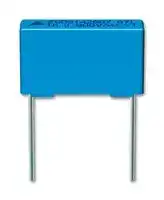
B32674D1155K000
Power Film Capacitor, Metallized PP, Radial Box - 2 Pin, 1.5 µF, ± 10%, DC Link, Through Hole
⚠️ Reference pricing provided. In case of supply shortages, we will connect you with our trusted procurement partners to ensure your project's continuity.
- Manufacturer: EPCOS
- Product type: Power Film Capacitors
- ESR: 0.0163ohm
- Capacitance: 1.5µF
- Voltage(DC): 750V
- Lead Spacing: 27.5mm
- Product Length: 31.5mm
- Dielectric Type: Metallized PP
- Humidity Rating: GRADE II (Test Condition A)
- Capacitor Mounting: Through Hole
- RMS Current (Irms): 6.5A
- Capacitor Terminals: PC Pin
- Typical Applications: DC Link
- Capacitance Tolerance: ± 10%
- Capacitor Case / Package: Radial Box - 2 Pin
- Operating Temperature Min: -40°C
| Delivery and price | |
|---|---|
| Units per pack | 5200 |
| Price | 1.07 € |
| Current stock | 10+ |
| Lead time | 30 days |
Datasheet

**==> picture [156 x 48] intentionally omitted <==**

## **Film Capacitors**

Metallized Polypropylene Film Capacitors (MKP)

**Series/Type: B32674 ... B32678** Date: June 2018

© EPCOS AG 2018. Reproduction, publication and dissemination of this publication, enclosures hereto and the information contained therein without EPCOS' prior express consent is prohibited.

EPCOS AG is a TDK Group Company.

~~eee~~ **Metallized polypropylene film capacitors (MKP) B32674 ... B32678 MKP DC link high power series**

## **Typical applications**

Frequency converters Industrial and high-end power supplies Solar inverters

## **Climatic**

Max. operating temperature: 105 °C (case) Climatic category (IEC 60068-1:2013): 40/105/56

## **Construction**

Dielectric: Polypropylene (MKP) Plastic case (UL 94 V-0) Epoxy resin sealing (UL 94 V-0)

## **Features**

- Capacitance value up to 270 μF High CV product, compact Good self-healing properties Ove ~~r-~~ voltage capability

Low losses with high current capability High reliability Long useful life AEC-Q200D compliant

## **Terminals**

Parallel wire leads, lead-free tinned 2-pin, 4-pin and 12-pin versions Standard lead lengths: 6 1 mm

## **Marking**

Manufacturer's logo and lot number, date code, rated capacitance (coded), capacitance tolerance (code letter), rated DC voltage

## **Delivery mode**

Bulk (untaped, lead length 6 1 mm)

Please read _Cautions and warnings_ and _Important notes_ at the end of this document.

Page 2 of 42

**B32674 ... B32678 MKP DC link high power series**

## **Dimensional drawings**

|~~2~~|~~2~~|~~ee~~||
|---|---|---|---|
|Number of wires<br>~~2~~|Lead spacing<br>±0.4<br>~~2~~|Lead diameter d1±0.05<br>~~ee~~|Type|
|2-pin<br>~~2~~|27.5<br>~~2~~|0.8<br>~~ee~~|B32674D|
|2-pin|37.5|1.0|B32676T|
|4-pin|37.5|1.2|B32676G|
|4-pin|37.5|1.2|B32676T|
|4-pin|52.5|1.2|B32678G|
|4-pin|52.5|1.2|B32678T|
|12-pin|52.5|1.2|B32678J|


## **Dimensional drawings 2-pin versions**

## **B32674D**

Lead spacing ±0.4: 27.5 Lead diameter d1: 0.8 ~~ee~~ (Dimensions in mm)

## **B32676T** (low profile)

**==> picture [236 x 37] intentionally omitted <==**

**----- Start of picture text -----**<br>
Lead spacing ±0.4: 37.5<br>Lead diameter d1: 1.0<br>a<br>**----- End of picture text -----**<br>


(Dimensions in mm)

Please read _Cautions and warnings_ and _Important notes_ at the end of this document.

Page 3 of 42

**==> picture [185 x 45] intentionally omitted <==**

**----- Start of picture text -----**<br>
B32674 ... B32678<br>_<br>MKP DC link high power series<br>**----- End of picture text -----**<br>


## **Dimensional drawings 4-pin versions**

## **B32676G, B32678G**

**==> picture [236 x 64] intentionally omitted <==**

**----- Start of picture text -----**<br>
B32676G B32678G<br>Lead spacing ±0.4: 37.5 52.5<br>Lead diameter d1: 1.2 1.2<br>=f<br>(Dimensions in mm)<br>**----- End of picture text -----**<br>


## **B32676T, B32678T** (low profile)

|~~=~~|||
|---|---|---|
|~~=~~|B32676T|B32678T|
|Lead spacing<br>±0.4:<br>Lead diameter d1:<br>~~=~~|37.5<br>1.2|52.5<br>1.2|


## **Dimensional drawing 12-pin version**

## **B32678J**

Lead spacing ±0.4: 52.5 Lead diameter d1: 1.2 ~~ee~~ (Dimensions in mm)

Please read _Cautions and warnings_ and _Important notes_ at the end of this document.

Page 4 of 42

**B32674 ... B32678 MKP DC link** � **high power series**

**==> picture [46 x 90] intentionally omitted <==**

## **Overview of available types**

|Lead spacing|27.5 mm|27.5 mm||||37.5 mm|37.5 mm||||
|---|---|---|---|---|---|---|---|---|---|---|
|Type|B32674|||||B32676|||||
|Page|7|||||9|||||
|VR (V DC)|300|450|630|750|875|300|450|630|750|875|
|CR (μF)|||||||||||
|0.47|||||||||||
|0.68|||||||||||
|1.0|||||||||||
|1.5|||||||||||
|2.0|||||||||||
|2.2|||||||||||
|2.7|||||||||||
|3.0|||||||||||
|3.3|||||||||||
|3.5|||||||||||
|4.0|||||||||||
|4.7|||||||||||
|5.0|||||||||||
|5.6|||||||||||
|6.0|||||||||||
|6.2|||||||||||
|6.8|||||||||||
|7.5|||||||||||
|8.0|||||||||||
|8.2|||||||||||
|9.0|||||||||||
|10|||||||||||
|12|||||||||||
|13|||||||||||
|14|||||||||||
|15|||||||||||
|20|||||||||||
|22|||||||||||
|25|||||||||||
|30|||||||||||
|35|||||||||||


Please read _Cautions and warnings_ and _Important notes_ at the end of this document.

Page 5 of 42

**==> picture [41 x 56] intentionally omitted <==**

**B32674 ... B32678 MKP DC link** � **high power series**

## **Overview of available types**

|Lead spacing|52.5 mm|||||
|---|---|---|---|---|---|
|Type|B32678|||||
|Page|11|||||
|VR (V DC)|300|450|630|750|875|
|CR (μF)||||||
|7.0||||||
|9.0||||||
|13||||||
|15||||||
|20||||||
|22||||||
|24||||||
|25||||||
|28||||||
|30||||||
|35||||||
|38||||||
|40||||||
|45||||||
|47||||||
|60||||||
|65||||||
|80||||||
|85||||||
|100||||||
|120||||||
|180||||||
|270||||||


Please read _Cautions and warnings_ and _Important notes_ at the end of this document.

Page 6 of 42

**B32674 MKP DC link** � **high power series**

**==> picture [36 x 42] intentionally omitted <==**

## **Ordering codes and packing units (lead spacing 27.5 mm)**

|CR1)<br>μF|Max. dimensions<br>w×h×l<br>mm|P1<br>mm|Ordering code<br>(composition see<br>below)|IRMS,max2)<br>70°C<br>10 kHz<br>A|ESRtyp<br>70°C<br>10 kHz<br>mΩ|ESLtyp3)<br>nH|tanδ<br>1 kHz<br>10-3|tanδ<br>10 kHz<br>10-3|pcs./<br>MOQ|
|---|---|---|---|---|---|---|---|---|---|
|VR,85°C= 300 V DC, Vop,70°||C=|450 V DC|||||||
|2.2<br>3.3<br>4.7<br>5.0<br>6.8<br>8.0<br>8.2<br>10.0<br>12.0|11.0×19.0×31.5<br>12.5×21.5×31.5<br>14.0×24.5×31.5<br>15.0×24.5×31.5<br>18.0×27.5×31.5<br>16.0×32.0×31.5<br>18.0×33.0×31.5<br>21.0×31.0×31.5<br>22.0×36.5×31.5|�<br>�<br>�<br>�<br>�<br>�<br>�<br>�<br>�|B32674D3225+000<br>B32674D3335+000<br>B32674D3475+000<br>B32674D3505+000<br>B32674D3685+000<br>B32674D3805+000<br>B32674D3825+000<br>B32674D3106+000<br>B32674D3126+000|5.0<br>7.0<br>8.5<br>9.0<br>11.5<br>12.5<br>13.0<br>14.5<br>17.0|18.1<br>12.2<br>8.9<br>8.4<br>6.3<br>5.6<br>5.5<br>4.6<br>4.0|16.0<br>19.0<br>21.0<br>21.0<br>24.0<br>27.0<br>27.0<br>27.0<br>31.0|0.7<br>0.7<br>0.7<br>0.7<br>0.7<br>0.7<br>0.7<br>0.8<br>0.8|4.1<br>4.1<br>4.2<br>4.2<br>4.4<br>4.5<br>4.5<br>4.6<br>4.9|1280<br>1120<br>1040<br>960<br>800<br>880<br>800<br>720<br>640|
|VR,85°C= 450 V DC, Vop,70°||C=|630 V DC|||||||
|1.5<br>2.2<br>3.3<br>4.7<br>5.0<br>5.6<br>6.0<br>6.8<br>7.5|11.0×19.0×31.5<br>12.5×21.5×31.5<br>15.0×24.5×31.5<br>18.0×27.5×31.5<br>16.0×32.0×31.5<br>18.0×33.0×31.5<br>21.0×31.0×31.5<br>22.0×36.5×31.5<br>22.0×36.5×31.5|�<br>�<br>�<br>�<br>�<br>�<br>�<br>�<br>�|B32674D4155+000<br>B32674D4225+000<br>B32674D4335+000<br>B32674D4475+000<br>B32674D4505+000<br>B32674D4565+000<br>B32674D4605+000<br>B32674D4685+000<br>B32674D4755+000|4.5<br>6.0<br>8.0<br>10.5<br>11.0<br>12.0<br>13.0<br>14.5<br>15.0|22.1<br>14.9<br>10.3<br>7.5<br>7.1<br>6.3<br>5.9<br>5.4<br>5.0|16.0<br>19.0<br>22.0<br>24.0<br>28.0<br>29.0<br>28.0<br>29.0<br>32.0|0.6<br>0.6<br>0.6<br>0.6<br>0.7<br>0.7<br>0.7<br>0.7<br>0.7|3.3<br>3.3<br>3.4<br>3.5<br>3.6<br>3.6<br>3.6<br>3.7<br>3.8|1280<br>1120<br>960<br>800<br>880<br>800<br>720<br>640<br>640|
|VR,85°C= 630 V DC, Vop,70°||C=|800 V DC|||||||
|1.0<br>1.5<br>2.2<br>3.3<br>4.7<br>5.0|11.0×19.0×31.5<br>12.5×21.5×31.5<br>15.0×24.5×31.5<br>16.0×32.0×31.5<br>22.0×36.5×31.5<br>22.0×36.5×31.5|�<br>�<br>�<br>�<br>�<br>�|B32674D6105+000<br>B32674D6155+000<br>B32674D6225+000<br>B32674D6335+000<br>B32674D6475+000<br>B32674D6505+000|4.0<br>5.5<br>7.5<br>10.0<br>13.5<br>14.5|26.1<br>17.9<br>12.4<br>8.5<br>6.0<br>5.8|17.0<br>19.0<br>21.0<br>28.0<br>31.0<br>31.0|0.6<br>0.6<br>0.6<br>0.6<br>0.6<br>0.6|2.7<br>2.7<br>2.7<br>2.8<br>3.0<br>3.0|1280<br>1120<br>960<br>880<br>640<br>640|


MOQ = Minimum Order Quantity, consisting of 4 packing units. Intermediate capacitance values are available on request.

## **Composition of ordering code**

- + = Capacitance tolerance code:

   - K = ±10%

   - J = ±5%

- 1) Capacitance value measured at 1 kHz

- 2) Max. ripple current IRMS at 70 °C at 10 kHz for a ΔT ≤20 °C when ΔESRtyp ≤±5%

- 3) ESL value measured at resonance frequency (see specific graphs of Z versus frequency)

Please read _Cautions and warnings_ and _Important notes_ at the end of this document.

Page 7 of 42

**B32674**

**==> picture [36 x 42] intentionally omitted <==**

## **MKP DC link** � **high power series**

## **Ordering codes and packing units (lead spacing 27.5 mm)**

|CR4)<br>μF|Max. dimensions<br>w×h×l<br>mm|P1<br>mm|Ordering code<br>(composition see<br>below)|IRMS,max5)<br>70°C<br>10 kHz<br>A|ESRtyp<br>70°C<br>10 kHz<br>mΩ|ESLtyp6)<br>nH|tanδ<br>1 kHz<br>10-3|tanδ<br>10 kHz<br>10-3|pcs./<br>MOQ|
|---|---|---|---|---|---|---|---|---|---|
|VR,85°C= 750 V DC, Vop,70||°C=|900 V DC|||||||
|0.68<br>1.0<br>1.5<br>2.2<br>3.3<br>4.0|11.0×19.0×31.5<br>12.5×21.5×31.5<br>14.0×24.5×31.5<br>18.0×27.5×31.5<br>21.0×31.0×31.5<br>22.0×36.5×31.5|�<br>�<br>�<br>�<br>�<br>�|B32674D1684+000<br>B32674D1105+000<br>B32674D1155+000<br>B32674D1225+000<br>B32674D1335+000<br>B32674D1405+000|3.5<br>4.5<br>6.5<br>8.5<br>11.0<br>13.0|34.7<br>24.2<br>16.3<br>11.3<br>7.9<br>6.7|17.0<br>18.0<br>22.0<br>24.0<br>28.0<br>32.0|0.5<br>0.5<br>0.6<br>0.6<br>0.6<br>0.6|2.4<br>2.5<br>2.5<br>2.5<br>2.6<br>2.7|1280<br>1120<br>1040<br>800<br>720<br>640|
|VR,85°C= 875 V DC, Vop,70||°C= 1050 V DC||||||||
|0.47<br>0.68<br>1.0<br>1.5<br>2.2<br>3.0|11.0×19.0×31.5<br>11.0×21.0×31.5<br>13.5×23.0×31.5<br>18.0×27.5×31.5<br>18.0×33.0×31.5<br>22.0×36.5×31.5|�<br>�<br>�<br>�<br>�<br>�|B32674D8474+000<br>B32674D8684+000<br>B32674D8105+000<br>B32674D8155+000<br>B32674D8225+000<br>B32674D8305+000|3.0<br>4.0<br>5.0<br>7.5<br>9.5<br>12.0|45.2<br>31.5<br>22.2<br>14.7<br>10.3<br>7.8|16.0<br>19.0<br>20.0<br>23.0<br>29.0<br>31.0|0.5<br>0.5<br>0.5<br>0.5<br>0.5<br>0.5|2.2<br>2.2<br>2.2<br>2.2<br>2.3<br>2.4|1280<br>1280<br>1040<br>800<br>800<br>640|


MOQ = Minimum Order Quantity, consisting of 4 packing units. Intermediate capacitance values are available on request.

## **Composition of ordering code**

- + = Capacitance tolerance code:

   - K = ±10%

   - J = ±5%

> 4) Capacitance value measured at 1 kHz

> 5) Max. ripple current IRMS at 70 °C at 10 kHz for a ΔT ≤20 °C when ΔESRtyp ≤±5%

> 6) ESL value measured at resonance frequency (see specific graphs of Z versus frequency)

Please read _Cautions and warnings_ and _Important notes_ at the end of this document.

Page 8 of 42

**B32676 MKP DC link** � **high power series**

**==> picture [42 x 90] intentionally omitted <==**

## **Ordering codes and packing units (lead spacing 37.5 mm)**

|CR1)<br>μF|Max. dimensions<br>w×h×l<br>mm|P1<br>mm|Ordering code<br>(composition see<br>below)|IRMS,max2)<br>70°C<br>10 kHz<br>A|ESRtyp<br>70°C<br>10 kHz<br>mΩ|ESLtyp3)<br>nH|tanδ<br>1 kHz<br>10-3|tanδ<br>10 kHz<br>10-3|pcs./<br>MOQ|
|---|---|---|---|---|---|---|---|---|---|
|VR,85|°C= 300 V DC, Vop,70°C=||450 V DC|||||||
|6.2<br>9.0<br>15.0<br>20.0<br>20.0<br>22.0<br>25.0<br>30.0<br>35.0|24.0×15.0×41.5<br>24.0×19.0×41.5<br>20.0×39.5×42.0<br>28.0×37.0×42.0<br>43.0×22.0×41.5<br>28.0×42.5×42.0<br>28.0×42.5×42.0<br>30.0×45.0×42.0<br>33.0×48.0×42.0|�<br>�<br>10.2<br>10.2<br>20.3<br>10.2<br>10.2<br>20.3<br>20.3|B32676T3625+000<br>B32676T3905+000<br>B32676G3156+000<br>B32676G3206+000<br>B32676T3206K000<br>B32676G3226+000<br>B32676G3256+000<br>B32676G3306+000<br>B32676G3356+000|8.0<br>10.0<br>16.0<br>20.0<br>19.5<br>21.5<br>22.5<br>26.0<br>29.5|12.6<br>9.1<br>5.4<br>4.0<br>4.0<br>3.8<br>3.4<br>2.8<br>2.5|18.0<br>19.0<br>10.0<br>11.0<br>13.0<br>11.0<br>12.0<br>12.0<br>13.0|1.1<br>1.1<br>1.1<br>1.1<br>1.1<br>1.2<br>1.2<br>1.2<br>1.2|8.2<br>8.3<br>8.3<br>8.4<br>8.3<br>8.5<br>8.6<br>8.7<br>8.8|1040<br>780<br>640<br>440<br>280<br>440<br>440<br>400<br>180|
|VR,85|°C= 450 V DC, Vop,70°C=||630 V DC|||||||
|4.0<br>4.7<br>8.2<br>10.0<br>13.0<br>15.0<br>20.0<br>25.0|24.0×15.0×41.5<br>24.0×19.0×41.5<br>20.0×39.5×42.0<br>20.0×39.5×42.0<br>43.0×22.0×41.5<br>28.0×42.5×42.0<br>30.0×45.0×42.0<br>33.0×48.0×42.0|�<br>�<br>10.2<br>10.2<br>20.3<br>10.2<br>20.3<br>20.3|B32676T4405+000<br>B32676T4475+000<br>B32676G4825+000<br>B32676G4106+000<br>B32676T4136K000<br>B32676G4156+000<br>B32676G4206K000<br>B32676G4256K000|7.0<br>8.0<br>13.5<br>14.5<br>17.5<br>20.0<br>24.0<br>28.0|15.5<br>13.2<br>7.8<br>6.4<br>5.0<br>4.4<br>3.3<br>2.8|19.0<br>18.0<br>9.0<br>11.0<br>13.0<br>11.0<br>13.0<br>14.0|1.0<br>1.0<br>1.0<br>1.0<br>1.0<br>1.0<br>1.0<br>1.0|6.6<br>6.6<br>6.7<br>6.7<br>6.6<br>6.8<br>6.9<br>7.1|1040<br>780<br>640<br>640<br>280<br>440<br>400<br>180|
|VR,85|°C= 630 V DC, Vop,70°C=||800 V DC|||||||
|2.7<br>3.5<br>6.8<br>7.5<br>8.2<br>9.0<br>10.0<br>12.0<br>14.0<br>15.0|24.0×15.0×41.5<br>24.0×19.0×41.5<br>20.0×39.5×42.0<br>20.0×39.5×42.0<br>28.0×37.0×42.0<br>43.0×22.0×41.5<br>28.0×42.5×42.0<br>28.0×42.5×42.0<br>30.0×45.0×42.0<br>33.0×48.0×42.0|�<br>�<br>10.2<br>10.2<br>10.2<br>20.3<br>10.2<br>10.2<br>20.3<br>20.3|B32676T6275+000<br>B32676T6355+000<br>B32676G6685+000<br>B32676G6755+000<br>B32676G6825+000<br>B32676T6905K000<br>B32676G6106+000<br>B32676G6126+000<br>B32676G6146+000<br>B32676G6156+000|7.0<br>8.0<br>13.5<br>14.5<br>16.0<br>16.5<br>18.5<br>20.0<br>23.0<br>25.0|17.7<br>14.1<br>7.4<br>6.6<br>6.1<br>5.7<br>5.1<br>4.4<br>3.7<br>3.5|20.0<br>19.0<br>10.0<br>12.0<br>11.0<br>13.0<br>11.0<br>12.0<br>14.0<br>14.0|0.8<br>0.8<br>0.8<br>0.8<br>0.8<br>0.8<br>0.8<br>0.8<br>0.8<br>0.8|5.1<br>5.1<br>5.2<br>5.2<br>5.2<br>5.1<br>5.2<br>5.3<br>5.3<br>5.4|1040<br>780<br>640<br>640<br>440<br>280<br>440<br>440<br>400<br>180|


MOQ = Minimum Order Quantity, consisting of 4 packing units. Intermediate capacitance values are available on request.

## **Composition of ordering code**

- + = Capacitance tolerance code:

   - K = ±10%

   - J = ±5%

- 1) Capacitance value measured at 1 kHz

- 2) Max. ripple current IRMS at 70 °C at 10 kHz for a ΔT ≤20 °C when ΔESRtyp ≤±5%

- 3) ESL value measured at resonance frequency (see specific graphs of Z versus frequency)

Please read _Cautions and warnings_ and _Important notes_ at the end of this document.

Page 9 of 42

**B32676 MKP DC link** � **high power series**

**==> picture [42 x 56] intentionally omitted <==**

## **Ordering codes and packing units (lead spacing 37.5 mm)**

|CR4)<br>μF|Max. dimensions<br>w×h×l<br>mm|P1<br>mm|Ordering code<br>(composition see<br>below)|IRMS,max5)<br>70°C<br>10 kHz<br>A|ESRtyp<br>70°C<br>10 kHz<br>mΩ|ESLtyp6)<br>nH|tanδ<br>1 kHz<br>10-3|tanδ<br>10 kHz<br>10-3|pcs./<br>MOQ|
|---|---|---|---|---|---|---|---|---|---|
|VR,85|°C= 750 V DC, Vop,70°C=||900 V DC|||||||
|2.0<br>2.7<br>4.7<br>5.6<br>6.8<br>9.0<br>10.0<br>12.0|24.0×15.0×41.5<br>24.0×19.0×41.5<br>20.0×39.5×42.0<br>20.0×39.5×42.0<br>28.0×37.0×42.0<br>30.0×45.0×42.0<br>30.0×45.0×42.0<br>33.0×48.0×42.0|�<br>�<br>10.2<br>10.2<br>10.2<br>20.3<br>20.3<br>20.3|B32676T1205+000<br>B32676T1275+000<br>B32676G1475+000<br>B32676G1565+000<br>B32676G1685+000<br>B32676G1905+000<br>B32676G1106+000<br>B32676G1126+000|6.0<br>7.5<br>12.0<br>13.0<br>15.5<br>19.5<br>20.5<br>23.0|22.7<br>16.7<br>9.5<br>8.2<br>6.7<br>5.1<br>4.7<br>4.0|18.0<br>19.0<br>10.0<br>11.0<br>11.0<br>12.0<br>13.0<br>14.0|0.8<br>0.8<br>0.8<br>0.8<br>0.8<br>0.8<br>0.8<br>0.8|4.6<br>4.6<br>4.6<br>4.7<br>4.7<br>4.7<br>4.8<br>4.8|1040<br>780<br>640<br>640<br>440<br>440<br>400<br>180|
|VR,85|°C= 875 V DC, Vop,70°C= 1050 V DC|||||||||
|1.5<br>2.0<br>3.3<br>4.0<br>4.7<br>6.8<br>7.5<br>10.0|24.0×15.0×41.5<br>24.0×19.0×41.5<br>20.0×39.5×42.0<br>20.0×39.5×42.0<br>28.0×37.0×42.0<br>28.0×42.5×42.0<br>30.0×45.0×42.0<br>33.0×48.0×42.0|�<br>�<br>10.2<br>10.2<br>10.2<br>10.2<br>20.3<br>20.3|B32676T8155+000<br>B32676T8205+000<br>B32676G8335+000<br>B32676G8405+000<br>B32676G8475+000<br>B32676G8685+000<br>B32676G8755+000<br>B32676G8106K000|5.5<br>7.0<br>10.5<br>12.0<br>13.5<br>17.0<br>19.0<br>22.5|26.2<br>19.6<br>12.0<br>9.9<br>8.6<br>6.0<br>5.4<br>4.3|18.0<br>19.0<br>9.0<br>11.0<br>10.0<br>12.0<br>13.0<br>14.0|0.7<br>0.7<br>0.7<br>0.7<br>0.7<br>0.7<br>0.7<br>0.7|4.1<br>4.1<br>4.1<br>4.1<br>4.1<br>4.2<br>4.2<br>4.3|1040<br>780<br>640<br>640<br>440<br>440<br>400<br>180|


MOQ = Minimum Order Quantity, consisting of 4 packing units. Intermediate capacitance values are available on request.

## **Composition of ordering code**

- + = Capacitance tolerance code:

   - K = ±10%

   - J = ±5%

> 4) Capacitance value measured at 1 kHz

> 5) Max. ripple current IRMS at 70 °C at 10 kHz for a ΔT ≤20 °C when ΔESRtyp ≤±5%

> 6) ESL value measured at resonance frequency (see specific graphs of Z versus frequency)

Please read _Cautions and warnings_ and _Important notes_ at the end of this document.

Page 10 of 42

**B32678 MKP DC link** � **high power series**

**==> picture [61 x 90] intentionally omitted <==**

## **Ordering codes and packing units (lead spacing 52.5 mm)**

|CR1)<br>μF|Max. dimensions<br>w×h×l<br>mm|P1<br>mm|Ordering code<br>(composition see<br>below)|IRMS,max2)<br>70°C<br>10 kHz<br>A|ESRtyp<br>70°C<br>10 kHz<br>mΩ|ESLtyp3)<br>nH|tanδ<br>1 kHz<br>10-3|tanδ<br>10 kHz<br>10-3|pcs./<br>MOQ|
|---|---|---|---|---|---|---|---|---|---|
|VR,85°C= 300 V DC, Vop,70°C=<br>450 V DC||||||||||
|30.0<br>40.0<br>47.0<br>60.0<br>80.0<br>80.0<br>100.0<br>270.0|43.0×24.0×57.5<br>30.0×45.0×57.5<br>35.0×50.0×57.5<br>35.0×50.0×57.5<br>45.0×57.0×57.5<br>130.0×24.0×57.5<br>60.0×45.0×57.5<br>130.0×58.0×57.5|20.3<br>20.3<br>20.3<br>20.3<br>20.3<br>20.3<br>20.3<br>20.3|B32678T3306K000<br>B32678G3406+000<br>B32678G3476+000<br>B32678G3606K000<br>B32678G3806+000<br>B32678J3806K000<br>B32678G3107+000<br>B32678J3277K000|22.5<br>28.0<br>33.0<br>37.0<br>47.0<br>51.0<br>48.0<br>108.0|3.9<br>3.0<br>2.6<br>2.1<br>1.6<br>1.4<br>1.4<br>0.5|13.0<br>12.0<br>13.0<br>15.0<br>18.0<br>4.0<br>19.0<br>6.0|1.5<br>1.5<br>1.5<br>1.6<br>1.6<br>1.5<br>1.6<br>1.6|11.8<br>12.3<br>12.5<br>12.9<br>13.5<br>11.7<br>13.5<br>13.8|560<br>280<br>108<br>108<br>140<br>80<br>200<br>40|
|VR,85°C= 450 V DC, Vop,70°C=<br>630 V DC||||||||||
|20.0<br>30.0<br>35.0<br>40.0<br>60.0<br>60.0<br>65.0<br>180.0|43.0×24.0×57.5<br>35.0×50.0×57.5<br>35.0×50.0×57.5<br>35.0×50.0×57.5<br>45.0×57.0×57.5<br>130.0×24.0×57.5<br>60.0×45.0×57.5<br>130.0×58.0×57.5|20.3<br>20.3<br>20.3<br>20.3<br>20.3<br>20.3<br>20.3<br>20.3|B32678T4206K000<br>B32678G4306+000<br>B32678G4356+000<br>B32678G4406K000<br>B32678G4606+000<br>B32678J4606K000<br>B32678G4656+000<br>B32678J4187K000|20.0<br>28.0<br>31.5<br>34.0<br>45.0<br>49.5<br>48.0<br>97.5|4.9<br>3.2<br>2.8<br>2.5<br>1.8<br>1.6<br>1.6<br>0.6|13.0<br>14.0<br>14.0<br>15.0<br>18.0<br>4.0<br>19.0<br>6.0|1.3<br>1.3<br>1.3<br>1.3<br>1.4<br>1.2<br>1.3<br>1.4|9.8<br>9.9<br>10.0<br>10.2<br>11.2<br>9.5<br>10.6<br>11.2|560<br>108<br>108<br>108<br>140<br>80<br>200<br>40|
|VR,85°C= 630 V DC, Vop,70°C=<br>800 V DC||||||||||
|13.0<br>20.0<br>25.0<br>38.0<br>40.0<br>45.0<br>120.0|43.0×24.0×57.5<br>35.0×50.0×57.5<br>35.0×50.0×57.5<br>130.0×24.0×57.5<br>45.0×57.0×57.5<br>60.0×45.0×57.5<br>130.0×58.0×57.5|20.3<br>20.3<br>20.3<br>20.3<br>20.3<br>20.3<br>20.3|B32678T6136K000<br>B32678G6206+000<br>B32678G6256+000<br>B32678J6386K000<br>B32678G6406+000<br>B32678G6456+000<br>B32678J6127K000|18.0<br>26.5<br>29.5<br>43.5<br>41.0<br>43.0<br>90.0|5.9<br>4.0<br>3.3<br>2.1<br>2.1<br>1.9<br>0.7|13.0<br>13.0<br>15.0<br>4.0<br>18.0<br>19.0<br>6.0|1.1<br>1.1<br>1.1<br>1.1<br>1.2<br>1.2<br>1.2|7.9<br>8.2<br>8.3<br>7.9<br>8.8<br>8.7<br>8.8|560<br>108<br>108<br>80<br>140<br>200<br>40|


MOQ = Minimum Order Quantity, consisting of 4 packing units. Intermediate capacitance values are available on request.

## **Composition of ordering code**

- + = Capacitance tolerance code:

K = ±10%

J = ±5%

> 1) Capacitance value measured at 1 kHz

> 2) Max. ripple current IRMS at 70 °C at 10 kHz for a ΔT ≤20 °C when ΔESRtyp ≤±5%

> 3) ESL value measured at resonance frequency (see specific graphs of Z versus frequency)

Please read _Cautions and warnings_ and _Important notes_ at the end of this document.

Page 11 of 42

**B32678**

**==> picture [61 x 57] intentionally omitted <==**

## **MKP DC link** � **high power series**

## **Ordering codes and packing units (lead spacing 52.5 mm)**

|CR4)<br>μF|Max. dimensions<br>w×h×l<br>mm|P1<br>mm|Ordering code<br>(composition see<br>below)|IRMS,max5)<br>70°C<br>10 kHz<br>A|ESRtyp<br>70°C<br>10 kHz<br>mΩ|ESLtyp6)<br>nH|tanδ<br>1 kHz<br>10-3|tanδ<br>10 kHz<br>10-3|pcs./<br>MOQ|
|---|---|---|---|---|---|---|---|---|---|
|VR,85°C= 750 V DC, Vop,70°C=<br>900 V DC||||||||||
|9.0<br>15.0<br>20.0<br>28.0<br>30.0<br>30.0<br>85.0|43.0×24.0×57.5<br>30.0×45.0×57.5<br>35.0×50.0×57.5<br>45.0×57.0×57.5<br>60.0×45.0×57.5<br>130.0×24.0×57.5<br>130.0×58.0×57.5|20.3<br>20.3<br>20.3<br>20.3<br>20.3<br>20.3<br>20.3|B32678T1905K000<br>B32678G1156K000<br>B32678G1206K000<br>B32678G1286+000<br>B32678G1306+000<br>B32678J1306K000<br>B32678J1856K000|16.5<br>23.0<br>28.0<br>37.5<br>39.5<br>40.5<br>82.5|7.2<br>4.5<br>3.5<br>2.5<br>2.4<br>2.3<br>0.9|13.0<br>14.0<br>15.0<br>18.0<br>19.0<br>4.0<br>6.0|1.0<br>1.0<br>1.0<br>1.0<br>1.0<br>1.0<br>1.0|6.8<br>7.0<br>7.2<br>7.4<br>7.3<br>6.8<br>7.4|560<br>280<br>108<br>140<br>200<br>80<br>40|
|VR,85°C= 875 V DC, Vop,70°C= 1050 V DC||||||||||
|7.0<br>15.0<br>22.0<br>22.0<br>24.0<br>65.0|43.0×24.0×57.5<br>35.0×50.0×57.5<br>45.0×57.0×57.5<br>130.0×24.0×57.5<br>60.0×45.0×57.5<br>130.0×58.0×57.5|20.3<br>20.3<br>20.3<br>20.3<br>20.3<br>20.3|B32678T8705K000<br>B32678G8156K000<br>B32678G8226+000<br>B32678J8226K000<br>B32678G8246+000<br>B32678J8656K000|15.5<br>26.5<br>35.0<br>39.0<br>38.0<br>78.0|8.2<br>4.0<br>2.9<br>2.6<br>2.6<br>1.0|13.0<br>15.0<br>17.0<br>5.0<br>19.0<br>6.0|0.9<br>0.9<br>1.0<br>0.9<br>0.9<br>1.0|6.0<br>6.3<br>6.5<br>6.0<br>6.4<br>6.5|560<br>108<br>140<br>80<br>200<br>40|


MOQ = Minimum Order Quantity, consisting of 4 packing units. Intermediate capacitance values are available on request.

## **Composition of ordering code**

- + = Capacitance tolerance code:

K = ±10%

J = ±5%

> 4) Capacitance value measured at 1 kHz

> 5) Max. ripple current IRMS at 70 °C at 10 kHz for a ΔT ≤20 °C when ΔESRtyp ≤±5%

> 6) ESL value measured at resonance frequency (see specific graphs of Z versus frequency)

Please read _Cautions and warnings_ and _Important notes_ at the end of this document.

Page 12 of 42

**B32674 ... B32678 MKP DC link** � **high power series**

**==> picture [46 x 90] intentionally omitted <==**

## **Technical data**

° Reference standard: IEC 61071:2007 and AEC-Q200D. All data given at T = 20 C, unless otherwise specified.

|wise specified.||||||
|---|---|---|---|---|---|
|Rated temperature TR|+85°C|||||
|Operating temperature range (case)|Max. operating temperature, Top,max<br>Upper category temperature Tmax<br>Lower categorytemperature Tmin<br>+105°C<br>+105°C<br>�40°C|||||
|Insulation resistance Rins<br>given as time constant<br>τ= CR�Rins, rel. humidity≤65%<br>(minimum as-delivered values)|τ> 10000 s (after 1 min)<br>For VR≥500 V measured at 500 V<br>For VR< 500 V measured at VR|||||
|DC voltage test between terminals(10 s)|1.5�VR|||||
|Voltage test terminal to case(10 s)|2110 V AC, 50 Hz|||||
|Pulse HandlingCapability (V/μs)|IP(A)/ C(μF)|||||
|Biased humidity<br>Limit values after test|1000 hours / 40°C / 93% relative humidity with VR,DC<br>Capacitance change |ΔC/C|<br>≤5%<br>Dissipation factor changeΔtanδ ≤0.002 (at 1 kHz)<br>Insulation resistance Rins<br>≥50% of minimum<br>as-delivered values|||||
|Reliability:<br>Failure rateλ<br>Service life tSL|1 fit (≤1�10-9/h) at 0.5�VR, 40°C<br>200 000 h at VR, 85°C<br>For conversion to other operating conditions and<br>temperatures, refer to chapter "Quality, 2 Reliability".|||||
|VR(V DC)|300|450|630|750|875|
|Continuous operation voltage<br>Vop(V DC)at 70°C|450|630|800|900|1050|
|Continuous operation voltage<br>Vop(V DC)at 85°C|300|450|630|750|875|
|For temperatures between<br>85°C and 100°C|1.2%/°C of Vopderating compared to Vopat 85°C|||||


## **Typical waveforms**

Restrictions:

**VR** : Maximum operating peak voltage of either polarity but of a non-reversing waveform, for which the capacitor has been designed for continuous operation.

Please read _Cautions and warnings_ and _Important notes_ at the end of this document.

Page 13 of 42

**==> picture [41 x 56] intentionally omitted <==**

**B32674 ... B32678 MKP DC link** � **high power series**

## **ûAC** ≤ **0.2** � **VR**

## **V : p, max**

|**Vp, max:**|||
|---|---|---|
|**Overvoltage**|**Maximum duration within one day**|**Observation**|
|1.1�VR<br>1.15�VR<br>1.2�VR<br>1.3�VR|30% of on-load duration<br>30 min.<br>5 min.<br>1 min.|System regulation<br>System regulation<br>System regulation<br>System regulation|


NOTE 1 An overvoltage equal to 1.5 � VR for 30 ms is permitted 1000 times during the life of the capacitor.

The amplitudes of the overvoltages that may be tolerated without significant reduction in the life time of the capacitor depend on their duration, the number of application and the capacitor temperature.

In addition these values assume that the overvoltages may appear when the internal temperature of the capacitor is less than 0 °C but within the temperature category.

NOTE 2 The average applied voltage must not be higher than the specified voltage.

## **Pulse handling capability**

"dV/dt" represents the maximum permissible voltage change per unit of time for non-sinusoidal voltages, expressed in V/μs.

## _Note:_

_The values of dV/dt and k0 provided below must not be exceeded in order to avoid damaging the capacitor. These parameters are given for isolated pulses in such a way that the heat generated by one pulse will be completely dissipated before applying the next pulse. For a train of pulses, please refer to the curves of permissible AC voltage-current versus frequency._

## **dV/dt values**

|**dV/dt values**||||||||||||||||
|---|---|---|---|---|---|---|---|---|---|---|---|---|---|---|---|
|Lead spacing|27.5 mm|||||37.5 mm|||||52.5 mm|||||
|Type|B32674|||||B32676|||||B32678|||||
|VR(V DC)|300|450|630|750|875|300|450|630|750|875|300|450|630|750|875|
|dV/dt in V/μs|40|75|100|125|150|22|54|73|85|100|15|35|50|60|70|


Please read _Cautions and warnings_ and _Important notes_ at the end of this document.

Page 14 of 42

**==> picture [420 x 18] intentionally omitted <==**

**----- Start of picture text -----**<br>
B32674<br>**----- End of picture text -----**<br>


## **MKP DC link** � **high power series**

**==> picture [36 x 42] intentionally omitted <==**

## **Characteristics curves**

Additional technical information can be found under "Design support" on www.epcos.com.

## **Impedance Z versus frequency f** (typical values) **Lead spacing 27.5 mm**

300 V DC

**ESR versus frequency f** (typical values)

**Lead spacing 27.5 mm** 300 V DC

**==> picture [62 x 52] intentionally omitted <==**

## **Impedance Z versus frequency f** (typical values) **Lead spacing 27.5 mm**

450 V DC

## **ESR versus frequency f** (typical values)

## **Lead spacing 27.5 mm**

450 V DC

**==> picture [66 x 52] intentionally omitted <==**

**==> picture [32 x 61] intentionally omitted <==**

Please read _Cautions and warnings_ and _Important notes_ at the end of this document.

Page 15 of 42

**==> picture [36 x 42] intentionally omitted <==**

**B32674 MKP DC link** � **high power series**

## **Characteristics curves**

Additional technical information can be found under "Design support" on www.epcos.com.

## **Impedance Z versus frequency f ESR versus frequency f** (typical values) (typical values) **Lead spacing 27.5 mm Lead spacing 27.5 mm**

**Lead spacing 27.5 mm** 630 V DC

630 V DC

**==> picture [66 x 52] intentionally omitted <==**

## **Impedance Z versus frequency f** (typical values) **Lead spacing 27.5 mm**

750 V DC

## **ESR versus frequency f** (typical values)

## **Lead spacing 27.5 mm**

750 V DC

**==> picture [62 x 52] intentionally omitted <==**

Please read _Cautions and warnings_ and _Important notes_ at the end of this document.

Page 16 of 42

**==> picture [420 x 18] intentionally omitted <==**

**----- Start of picture text -----**<br>
B32674<br>**----- End of picture text -----**<br>


## **MKP DC link** � **high power series**

**==> picture [36 x 42] intentionally omitted <==**

## **Characteristics curves**

Additional technical information can be found under "Design support" on www.epcos.com.

## **Impedance Z versus frequency f** (typical values) **Lead spacing 27.5 mm** 875 V DC

## **ESR versus frequency f** (typical values)

## **Lead spacing 27.5 mm**

875 V DC

**==> picture [38 x 61] intentionally omitted <==**

**==> picture [39 x 47] intentionally omitted <==**

Please read _Cautions and warnings_ and _Important notes_ at the end of this document.

Page 17 of 42

**==> picture [42 x 56] intentionally omitted <==**

**B32676 MKP DC link** � **high power series**

## **Characteristics curves**

Additional technical information can be found under "Design support" on www.epcos.com.

## **Impedance Z versus frequency f** (typical values) **Lead spacing 37.5 mm**

300 V DC

**ESR versus frequency f** (typical values)

**Lead spacing 37.5 mm** 300 V DC

**==> picture [42 x 41] intentionally omitted <==**

**==> picture [54 x 36] intentionally omitted <==**

**==> picture [34 x 87] intentionally omitted <==**

## **Impedance Z versus frequency f** (typical values)

## **Lead spacing 37.5 mm**

450 V DC

## **ESR versus frequency f** (typical values)

## **Lead spacing 37.5 mm**

450 V DC

**==> picture [34 x 86] intentionally omitted <==**

Please read _Cautions and warnings_ and _Important notes_ at the end of this document.

Page 18 of 42

**==> picture [420 x 18] intentionally omitted <==**

**----- Start of picture text -----**<br>
B32676<br>**----- End of picture text -----**<br>


## **MKP DC link** � **high power series**

**==> picture [42 x 90] intentionally omitted <==**

## **Characteristics curves**

Additional technical information can be found under "Design support" on www.epcos.com.

## **Impedance Z versus frequency f** (typical values) **Lead spacing 37.5 mm**

630 V DC

## **ESR versus frequency f** (typical values)

## **Lead spacing 37.5 mm** 630 V DC

**==> picture [73 x 52] intentionally omitted <==**

**==> picture [34 x 86] intentionally omitted <==**

## **Impedance Z versus frequency f** (typical values) **Lead spacing 37.5 mm**

750 V DC

## **ESR versus frequency f** (typical values)

## **Lead spacing 37.5 mm**

750 V DC

**==> picture [54 x 52] intentionally omitted <==**

Please read _Cautions and warnings_ and _Important notes_ at the end of this document.

Page 19 of 42

**==> picture [42 x 56] intentionally omitted <==**

**B32676 MKP DC link** � **high power series**

## **Characteristics curves**

Additional technical information can be found under "Design support" on www.epcos.com.

## **Impedance Z versus frequency f ESR versus frequency f** (typical values) (typical values) **Lead spacing 37.5 mm Lead spacing 37.5 mm** 875 V DC 875 V DC

## **Lead spacing 37.5 mm** 875 V DC

**==> picture [73 x 52] intentionally omitted <==**

**==> picture [36 x 84] intentionally omitted <==**

Please read _Cautions and warnings_ and _Important notes_ at the end of this document.

Page 20 of 42

**==> picture [420 x 18] intentionally omitted <==**

**----- Start of picture text -----**<br>
B32678<br>**----- End of picture text -----**<br>


## **MKP DC link** � **high power series**

**==> picture [61 x 90] intentionally omitted <==**

## **Characteristics curves**

Additional technical information can be found under "Design support" on www.epcos.com.

## **Impedance Z versus frequency f** (typical values) **Lead spacing 52.5 mm**

300 V DC

**ESR versus frequency f** (typical values)

**Lead spacing 52.5 mm** 300 V DC

**==> picture [54 x 36] intentionally omitted <==**

## **Impedance Z versus frequency f** (typical values) **Lead spacing 52.5 mm**

450 V DC

## **ESR versus frequency f** (typical values)

## **Lead spacing 52.5 mm** 450 V DC

**==> picture [62 x 35] intentionally omitted <==**

**==> picture [74 x 36] intentionally omitted <==**

Please read _Cautions and warnings_ and _Important notes_ at the end of this document.

Page 21 of 42

**B32678 MKP DC link** � **high power series**

**==> picture [61 x 57] intentionally omitted <==**

## **Characteristics curves**

Additional technical information can be found under "Design support" on www.epcos.com.

## **Impedance Z versus frequency f ESR versus frequency f** (typical values) (typical values) **Lead spacing 52.5 mm Lead spacing 52.5 mm**

**Lead spacing 52.5 mm** 630 V DC

630 V DC

**==> picture [62 x 41] intentionally omitted <==**

**==> picture [73 x 36] intentionally omitted <==**

**==> picture [36 x 59] intentionally omitted <==**

## **Impedance Z versus frequency f** (typical values) **Lead spacing 52.5 mm**

750 V DC

## **ESR versus frequency f** (typical values)

## **Lead spacing 52.5 mm**

750 V DC

**==> picture [42 x 41] intentionally omitted <==**

**==> picture [54 x 36] intentionally omitted <==**

Please read _Cautions and warnings_ and _Important notes_ at the end of this document.

Page 22 of 42

**==> picture [420 x 18] intentionally omitted <==**

**----- Start of picture text -----**<br>
B32678<br>**----- End of picture text -----**<br>


## **MKP DC link** � **high power series**

**==> picture [61 x 90] intentionally omitted <==**

## **Characteristics curves**

Additional technical information can be found under "Design support" on www.epcos.com.

## **Impedance Z versus frequency f** (typical values) **Lead spacing 52.5 mm**

875 V DC

**ESR versus frequency f** (typical values)

## **Lead spacing 52.5 mm** 875 V DC

**==> picture [62 x 41] intentionally omitted <==**

**==> picture [73 x 36] intentionally omitted <==**

## **Impedance Z versus frequency f** (typical values) **Lead spacing 52.5 mm (12 pins)**

300 V DC, 450 V DC, 630 V DC, 750 V DC, 875 V DC

## **ESR versus frequency f** (typical values)

## **Lead spacing 52.5 mm (12 pins)**

300 V DC, 450 V DC, 630 V DC, 750 V DC, 875 V DC

**==> picture [54 x 52] intentionally omitted <==**

**==> picture [36 x 82] intentionally omitted <==**

Please read _Cautions and warnings_ and _Important notes_ at the end of this document.

Page 23 of 42

## **B32674 MKP DC link high power series**

## **Characteristics curves**

## **Permissible current IRMS versus frequency f at 70** ° **C Lead spacing 27.5 mm**

B32674D*

Please read _Cautions and warnings_ and _Important notes_ at the end of this document.

Page 24 of 42

**B32676**

**MKP DC link** � **high power series**

**==> picture [42 x 90] intentionally omitted <==**

## **Characteristics curves**

## **Permissible current IRMS versus frequency f at 70** ° **C**

## **Lead spacing 37.5 mm**

B32676G/T*

Please read _Cautions and warnings_ and _Important notes_ at the end of this document.

Page 25 of 42

**B32678 MKP DC link** � **high power series**

**==> picture [61 x 57] intentionally omitted <==**

## **Characteristics curves**

## **Permissible current IRMS versus frequency f at 70** ° **C**

## **Lead spacing 52.5 mm**

B32678G/T*

**==> picture [40 x 184] intentionally omitted <==**

## B32678J*

**==> picture [40 x 187] intentionally omitted <==**

Please read _Cautions and warnings_ and _Important notes_ at the end of this document.

Page 26 of 42

**B32674 ... B32678 MKP DC link** � **high power series**

**==> picture [46 x 90] intentionally omitted <==**

## **Curves characteristics (IRMS derating versus temperature)**

Maximum IRMS current as function of the ambient temperature: IRMS (TA) = Factor × IRMS (70 °C)

Please read _Cautions and warnings_ and _Important notes_ at the end of this document.

Page 27 of 42

**B32674 ... B32678**

**==> picture [41 x 56] intentionally omitted <==**

## **MKP DC link** � **high power series**

**Heat transference for self heating calculation**

**==> picture [86 x 94] intentionally omitted <==**

Figure 1 (2-pin, 4-pin)

**==> picture [210 x 133] intentionally omitted <==**

Figure 2 (12-pin)

|**Box dimensions**|**Box dimensions**||**Equivalent heat**<br>**coefficient**|
|---|---|---|---|
|**w (mm)**|**h (mm)**|**l (mm)**|**G (mW/**°**C)**|
|11.0<br>11.0<br>12.5<br>13.5<br>14.0<br>15.0<br>16.0<br>18.0<br>18.0<br>19.0<br>20.0<br>21.0<br>22.0|19.0<br>21.0<br>21.5<br>23.0<br>24.5<br>24.5<br>32.0<br>27.5<br>33.0<br>30.0<br>11.0<br>31.0<br>36.5|31.5<br>31.5<br>31.5<br>31.5<br>31.5<br>31.5<br>31.5<br>31.5<br>31.5<br>31.5<br>31.5<br>31.5<br>31.5|25<br>28<br>30<br>32<br>35<br>36<br>45<br>44<br>48<br>48<br>65<br>51<br>58|
|12.0<br>14.0<br>16.0<br>18.0<br>20.0<br>24.0<br>24.0<br>28.0<br>28.0<br>30.0<br>33.0<br>43.0|22.0<br>25.0<br>28.5<br>32.5<br>39.5<br>19.0<br>15.0<br>37.0<br>42.5<br>45.0<br>48.0<br>22.0|41.5<br>41.5<br>41.5<br>41.5<br>42.0<br>41.5<br>41.5<br>42.0<br>42.0<br>42.0<br>42.0<br>41.5|70<br>43<br>50<br>59<br>72<br>50<br>44<br>83<br>90<br>100<br>110<br>80|
|30.0<br>35.0<br>43.0<br>45.0<br>60.0<br>130.0<br>130.0|45.0<br>50.0<br>24.0<br>57.0<br>45.0<br>24.0<br>58.0|57.5<br>57.5<br>57.5<br>57.5<br>57.5<br>57.5<br>57.5|125<br>145<br>103<br>185<br>192<br>200<br>300|


The equivalent heat coefficient **"G (mW/ºC)"** is given for measuring the temperature on the lateral surface of the plastic box as figure1 shows. By using a thermocouple and avoiding effect of radiation and convection the temperature measured during operation conditions should be a result of the dissipated power divided by the equivalent heat coefficient.

Please read _Cautions and warnings_ and _Important notes_ at the end of this document.

Page 28 of 42

**B32674 ... B32678 MKP DC link** � **high power series**

**==> picture [46 x 90] intentionally omitted <==**

## **Self Heating by power dissipation and equivalent heat coefficient**

The IRMS and consequently the power dissipation must be limited during operation in order to not exceed the maximum limit of ΔT allowed for this series. ΔTmax given for this series is equal or lower than 20 °C at rated temperature (70 °C), for higher ambient temperatures ΔTmax (T) will have the same derating factor than IRMS versus temperature and then an equivalent derating as per: ΔTmax (T) = (Factor)[2] × ΔT (70 °C).

For any particular IRMS the ΔT may be calculated by:

ΔT (°C) = Pdis (mW) / G(mW/°C).

Where ΔT (°C) is the difference between the temperature measured on the box (see figure 1) and the ambient temperature when capacitor is working during normal operation;

ΔT (°C) = Top (°C) � TA (°C).

It represents the increasing of temperature provoked by the IRMS during operation.

° G (mW/ C) is the equivalent heat coefficient described above and Pdis (mW) is the dissipated power defined by: Pdis (mW) = ESRtyp (mΩ) × IRMS[2] (ARMS).

## **Example for thermal calculation:**

We will take as reference B32678G8156K (15 μF/875 V) type for thermal calculation. Considering the following load and capacitor characteristics:

IRMS: 15 ARMS at 20 kHz TA: 85 ºC 35 × 50 × 57.5 box G (mW/ºC): 145

Then we have to find the ESRtyp at 20 kHz what is approximately 4.0 mΩ.

So according to Pdis (mW) = ESRtyp (mΩ) × IRMS[2] (ARMS) we have the following: Pdis (mW) = 4.0 mΩ ×15 ARMS[2] = 900 mW. And as per ΔT (°C) = Pdis (mW) / G (mW/°C) we have the following: ΔT (°C) = 900 (mW) / 145 (mW/°C) = 6.2 °C. What is below of the ΔTmax (85 °C) = (Factor)[2] × ΔT (70 °C) = (0.7)[2] × 20 °C = 9.8 °C.

On the other hand we may confirm that max IRMS at 20 kHz at 70 °C = 26.5 ARMS.

And then max IRMS for 85 °C of ambient temperature is defined as follows: IRMS (85 °C) = Factor × IRMS (70 °C) = 0.7 × 26.5 ARMS = 18.55 ARMS.

What confirms once again that IRMS (15 ARMS at 20 kHz at 85 °C) is below the max specified for such frequency and ambient temperature.

Please read _Cautions and warnings_ and _Important notes_ at the end of this document.

Page 29 of 42

**==> picture [41 x 56] intentionally omitted <==**

**B32674 ... B32678 MKP DC link** � **high power series**

## **Life time expectancy - typical curve**

B3267*3/4/6/1/8 (300 V DC / 450 V DC / 630 V DC / 750 V DC / 875 V DC)

Note: Confidence level of 98%

Please read _Cautions and warnings_ and _Important notes_ at the end of this document.

Page 30 of 42

**B32674 ... B32678 MKP DC link** � **high power series**

**==> picture [46 x 90] intentionally omitted <==**

## **Testing and Standards**

|**Test**|**Reference**|**Conditions of test**|**Conditions of test**|**Performance**<br>**requirements**|
|---|---|---|---|---|
|Electrical<br>parameters<br>(Routine<br>test)|IEC61071:2007|Voltage between terminals,<br>1.5 VR, during 10 s<br>Insulation resistance, Rinsat VRif<br>VR< 500 V or 500 V if VR≥500 V<br>Capacitance, C at 1 kHz<br>(room temperature)<br>Dissipation factor, tanδat 1/10 kHz<br>(room temperature)||Within specified limits|
|Robustness<br>of termina-<br>tions<br>(Type test)|IEC<br>60068-2-21:2006|Tensile strength (test Ua1)<br>Wire diameter<br>Tensile force||Capacitance and tanδ<br>within specified limits|
|||0.5 < d1≤0.8 mm<br>0.8 < d1≤1.25<br>mm|10 N<br>20 N||
|Resistance<br>to soldering<br>heat<br>(Type test)|IEC<br>60068-2-20:2008,<br>test Tb,<br>method 1A|Solder bath temperature at 260±5°C,<br>immersion for 10 seconds||�ΔC/C0�≤2%<br>�Δtanδ�≤0.002|
|Rapid<br>change of<br>temperature<br>(Type test)|IEC<br>60384-16:2005|TA= lower category temperature<br>TB= upper category temperature<br>Five cycles, duration t = 30 min.||�ΔC/C0�≤2%<br>�Δtanδ�≤0.002<br>Rins≥50% of initial limit|
|Vibration<br>(Type test)|IEC<br>60384-16:2005|Test FC: vibration sinusoidal<br>Displacement: 0.75 mm<br>Accleration: 98 m/s2<br>Frequency: 10 Hz ... 500 Hz<br>Test duration: 3 orthogonal axes,<br>2 hours each axe||No visible damage|
|Bump<br>(Type test)|IEC<br>60384-16:2005|Test Eb: Total 4000 bumps with<br>390 m/s2 mounted on PCB<br>Duration: 6 ms||No visible damage<br>�ΔC/C0�≤2%<br>�Δtanδ�≤0.002<br>Rins≥50% of initial limit|
|Climatic<br>sequence<br>(Type test)|IEC<br>60384-16:2005|Dry heat Tb / 16 h<br>Damp heat cyclic, 1st cycle<br>+55°C / 24 h / 95% ... 100% RH<br>Cold Ta / 2 h<br>Damp heat cyclic, 5 cycles<br>+55°C / 24 h / 95% ... 100% RH||No visible damage<br>�ΔC/C0�≤3%<br>�Δtanδ�≤0.001<br>Rins≥50% of initial limit|


Please read _Cautions and warnings_ and _Important notes_ at the end of this document.

Page 31 of 42

**==> picture [41 x 56] intentionally omitted <==**

**B32674 ... B32678 MKP DC link** � **high power series**

|**Test**|**Reference**|**Conditions of test**|**Performance**<br>**requirements**|
|---|---|---|---|
|Damp heat,<br>steady state<br>(Type test)|IEC<br>60384-16:2005|Test Ca<br>40°C / 93% RH / 56 days|No visible damage<br>�ΔC/C0�≤5%<br>�Δtanδ�≤0.005<br>Rins≥50% of initial limit|
|Endurance<br>(Type test)|IEC61071:2007|70°C / 1.4 VR/ 250 hours or<br>Top/ 1.4 Vop/ 250 hours<br>+ 1000 discharges at 1.4 IR<br>+70°C / 1.4 VR/ 250 hours or<br>Top/ 1.4 Vop/ 250 hours|No visible damage<br>�ΔC/C0�≤3% at 1 kHz<br>�Δtanδ�≤0.015 at<br>10 kHz|
|Endurance<br>(Type test)|IEC<br>60384-16:2005|70°C / 1.25 VR/ 1000 hours or<br>85°C / 1.25 Vop/ 1000 hours or<br>100°C / 1.25 Vop/ 1000 hours|No visible damage<br>�ΔC/C0�≤5% at 1 kHz<br>�Δtanδ�≤0.005<br>Rins≥50% of initial limit|


## **Mounting guidelines**

## **1 Soldering**

## **1.1 Solderability of leads**

The solderability of terminal leads is tested to IEC 60068-2-20, test Ta, method 1.

Before a solderability test is carried out, terminals are subjected to accelerated ageing (to IEC 60068-2-2, test Ba: 4 h exposure to dry heat at 155 °C). Since the ageing temperature is far higher than the upper category temperature of the capacitors, the terminal wires should be cut off from the capacitor before the ageing procedure to prevent the solderability being impaired by the products of any capacitor decomposition that might occur.

|Solder bath temperature|235±5°C|
|---|---|
|Solderingtime|2.0±0.5 s|
|Immersion depth|2.0 +0/�0.5 mm from capacitor bodyor seating plane|
|Evaluation criteria:<br>Visual inspection|Wetting of wire surface by new solder≥90%,<br>free-flowingsolder|


Please read _Cautions and warnings_ and _Important notes_ at the end of this document.

Page 32 of 42

**B32674 ... B32678 MKP DC link** � **high power series**

**==> picture [46 x 90] intentionally omitted <==**

**1.2 Resistance to soldering heat** Resistance to soldering heat is tested to IEC 60068-2-20, test Tb, method 1. Conditions:

|Series|Series|Series|Series|Series|Series|Series|Series|Solder bath temperature|Solderingtime|
|---|---|---|---|---|---|---|---|---|---|
|MKT|boxed (except 2.5×6.5×7.2 mm)<br>coated<br>uncoated(lead spacing>10 mm)|||||||260±5°C|10±1 s|
|MFP<br>MKP|(lead spacing>7.5 mm)|||||||||
|MKT|boxed(case 2.5×6.5×7.2 mm)||||||||5±1 s|
|MKP<br>MKT|(lead spacing≤7.5 mm)<br>uncoated (lead spacing≤10 mm)<br>insulated (B32559)||||||||<4 s<br>recommended soldering<br>profile for MKT uncoated<br>(lead spacing≤10 mm) and<br>insulated(B32559)|
|||||||||||
|||||||||||
|||||||||||
|||||||||||
|||||||||||
|||||||||||
|||||||||||
|||||||||||
|||||||||||
|Immersion depth||||||||2.0 +0/�0.5 mm from capacitor bodyor seating plane||
|Shield||||||||Heat-absorbing board, (1.5±0.5) mm thick, between<br>capacitor bodyand liquid solder||
|Evaluation criteria:<br>Visual inspection<br>ΔC/C0<br>tanδ||||||||No visible damage<br>2% for MKT/MKP/MFP<br>5% for EMI suppression capacitors<br>As specified in sectional specification||


Please read _Cautions and warnings_ and _Important notes_ at the end of this document.

Page 33 of 42

**B32674 ... B32678** ~~i~~

## **MKP DC link high power series**

## **1.3 General notes on soldering**

Permissible heat exposure loads on film capacitors are primarily characterized by the upper category temperature Tmax. Long exposure to temperatures above this type-related temperature limit can lead to changes in the plastic dielectric and thus change irreversibly a capacitor's electrical characteristics. For short exposures (as in practical soldering processes) the heat load (and thus the possible effects on a capacitor) will also depend on other factors like:

- Pre-heating temperature and time

- Forced cooling immediately after soldering

- Terminal characteristics:

- diameter, length, thermal resistance, special configurations (e.g. crimping)

- Height of capacitor above solder bath

- Shadowing by neighboring components

- Additional heating due to heat dissipation by neighboring components

- Use of solder-resist coatings

The overheating associated with some of these factors can usually be reduced by suitable countermeasures. For example, if a pre-heating step cannot be avoided, an additional or reinforced cooling process may possibly have to be included.

## **EPCOS recommendations**

As a reference, the recommended wave soldering profile for our film capacitors is as follows:

Please read _Cautions and warnings_ and _Important notes_ at the end of this document.

Page 34 of 42

**B32674 ... B32678** ~~a~~

## **MKP DC link**

**==> picture [97 x 12] intentionally omitted <==**

**----- Start of picture text -----**<br>
high power series<br>**----- End of picture text -----**<br>


Body temperature should follow the description below:

MKP capacitor

During pre-heating: Tp ≤110 °C

During soldering: Ts ≤120 °C, ts ≤45 s

MKT capacitor

During pre-heating: Tp ≤125 °C

During soldering: Ts ≤160 °C, ts ≤45 s

When SMD components are used together with leaded ones, the film capacitors should not pass into the SMD adhesive curing oven. The leaded components should be assembled after the SMD curing step.

Leaded film capacitors are not suitable for reflow soldering.

In order to ensure proper conditions for manual or selective soldering, the body temperature of the capacitor (Ts) must be ≤120 °C.

One recommended condition for manual soldering is that the tip of the soldering iron should be <360 °C and the soldering contact time should be no longer than 3 seconds.

For uncoated MKT capacitors with lead spacings ≤10 mm (B32560/B32561) the following measures are recommended:

pre-heating to not more than 110 °C in the preheater phase

rapid cooling after soldering

Please refer to EPCOS Film Capacitor Data Book in case more details are needed.

Please read _Cautions and warnings_ and _Important notes_ at the end of this document.

Page 35 of 42

**==> picture [41 x 56] intentionally omitted <==**

## **B32674 ... B32678**

**MKP DC link** � **high power series**

## **Cautions and warnings**

**==> picture [7 x 7] intentionally omitted <==**

**==> picture [7 x 7] intentionally omitted <==**

**==> picture [7 x 7] intentionally omitted <==**

**==> picture [7 x 7] intentionally omitted <==**

**==> picture [7 x 7] intentionally omitted <==**

**==> picture [7 x 7] intentionally omitted <==**

**==> picture [7 x 7] intentionally omitted <==**

**==> picture [7 x 7] intentionally omitted <==**

**==> picture [7 x 7] intentionally omitted <==**

**==> picture [7 x 7] intentionally omitted <==**

**==> picture [7 x 7] intentionally omitted <==**

**==> picture [7 x 7] intentionally omitted <==**

- Do not exceed the upper category temperature (UCT). Do not apply any mechanical stress to the capacitor terminals. Avoid any compressive, tensile or flexural stress.

- Do not move the capacitor after it has been soldered to the PC board. Do not pick up the PC board by the soldered capacitor.

- Do not place the capacitor on a PC board whose PTH hole spacing differs from the specified lead spacing.

- Do not exceed the specified time or temperature limits during soldering. Avoid external energy inputs, such as fire or electricity. Avoid overload of the capacitors.

Consult us if application is with severe temperature and humidity condition.

- There are no serviceable or repairable parts inside the capacitor. Opening the capacitor or any attempts to open or repair the capacitor will void the warranty and liability of EPCOS. Please note that the standards referred to in this publication may have been revised in the meantime.

The table below summarizes the safety instructions that must always be observed. A detailed description can be found in the relevant sections of the chapters "General technical information" and "Mounting guidelines".

|Topic|Safety information|Reference chapter<br>"General technical<br>information"|
|---|---|---|
|Storage<br>conditions|Make sure that capacitors are stored within the specified<br>range of time, temperature and humidityconditions.|4.5<br>"Storage conditions"|
|Flammability|Avoid external energy, such as fire or electricity (passive<br>flammability), avoid overload of the capacitors (active<br>flammability)and consider the flammabilityof materials.|5.3<br>"Flammability"|
|Resistance to<br>vibration|Do not exceed the tested ability to withstand vibration.<br>The capacitors are tested to IEC 60068-2-6:2007.<br>EPCOS offers film capacitors specially designed for<br>operation under more severe vibration regimes such as<br>those found in automotive applications. Consult our<br>catalog"Film Capacitors for Automotive Electronics".|5.2<br>"Resistance to<br>vibration"|
||||
|Topic|Safety information|Reference chapter<br>"Mounting guidelines"|
|Soldering|Do not exceed the specified time or temperature limits<br>duringsoldering.|1 "Soldering"|
|Cleaning|Use onlysuitable solvents for cleaningcapacitors.|2 "Cleaning"|


Please read _Cautions and warnings_ and _Important notes_ at the end of this document.

Page 36 of 42

**B32674 ... B32678 MKP DC link** � **high power series**

**==> picture [46 x 90] intentionally omitted <==**

|Topic|Safety information|Reference chapter<br>"Mounting guidelines"|
|---|---|---|
|Embedding of<br>capacitors in<br>finished<br>assemblies|When embedding finished circuit assemblies in plastic<br>resins, chemical and thermal influences must be taken<br>into account.<br>Caution: Consult us first, if you also wish to embed other<br>uncoated component types!|3 "Embedding of<br>capacitors in finished<br>assemblies"|


## **Display of ordering codes for EPCOS products**

The ordering code for one and the same product can be represented differently in data sheets, data books, other publications and the website of EPCOS, or in order-related documents such as shipping notes, order confirmations and product labels. **The varying representations of the ordering codes are due to different processes employed and do not affect the specifications of the respective products** . Detailed information can be found on the Internet under www.epcos.com/orderingcodes.

Please read _Cautions and warnings_ and _Important notes_ at the end of this document.

Page 37 of 42

**==> picture [41 x 56] intentionally omitted <==**

## **B32674 ... B32678 MKP DC link** � **high power series**

## **Symbols and terms**

|Symbol|English|German|
|---|---|---|
|α<br>αC<br>A<br>βC<br>C<br>CR<br>ΔC<br>ΔC/C<br>ΔC/CR<br>dt<br>Δt<br>ΔT<br>Δtanδ<br>ΔV<br>dV/dt<br>ΔV/Δt<br>E<br>ESL<br>ESR<br>f<br>f1<br>f2<br>fr<br>FD<br>FT<br>i<br>IC|Heat transfer coefficient<br>Temperature coefficient of capacitance<br>Capacitor surface area<br>Humidity coefficient of capacitance<br>Capacitance<br>Rated capacitance<br>Absolute capacitance change<br>Relative capacitance change (relative<br>deviation of actual value)<br>Capacitance tolerance (relative deviation<br>from rated capacitance)<br>Time differential<br>Time interval<br>Absolute temperature change<br>(self-heating)<br>Absolute change of dissipation factor<br>Absolute voltage change<br>Time differential of voltage function (rate<br>of voltage rise)<br>Voltage change per time interval<br>Activation energy for diffusion<br>Self-inductance<br>Equivalent series resistance<br>Frequency<br>Frequency limit for reducing permissible<br>AC voltage due to thermal limits<br>Frequency limit for reducing permissible<br>AC voltage due to current limit<br>Resonant frequency<br>Thermal acceleration factor for diffusion<br>Derating factor<br>Current (peak)<br>Category current (max. continuous<br>current)|Wärmeübergangszahl<br>Temperaturkoeffizient der Kapazität<br>Kondensatoroberfläche<br>Feuchtekoeffizient der Kapazität<br>Kapazität<br>Nennkapazität<br>Absolute Kapazitätsänderung<br>Relative Kapazitätsänderung (relative<br>Abweichung vom Ist-Wert)<br>Kapazitätstoleranz (relative Abweichung<br>vom Nennwert)<br>Differentielle Zeit<br>Zeitintervall<br>Absolute Temperaturänderung<br>(Selbsterwärmung)<br>Absolute Änderung des Verlustfaktors<br>Absolute Spannungsänderung<br>Differentielle Spannungsänderung<br>(Spannungsflankensteilheit)<br>Spannungsänderung pro Zeitintervall<br>Aktivierungsenergie zur Diffusion<br>Eigeninduktivität<br>Ersatz-Serienwiderstand<br>Frequenz<br>Grenzfrequenz für thermisch bedingte<br>Reduzierung der zulässigen<br>Wechselspannung<br>Grenzfrequenz für strombedingte<br>Reduzierung der zulässigen<br>Wechselspannung<br>Resonanzfrequenz<br>Therm. Beschleunigungsfaktor zur<br>Diffusion<br>Deratingfaktor<br>Stromspitze<br>Kategoriestrom (max. Dauerstrom)|


Please read _Cautions and warnings_ and _Important notes_ at the end of this document.

Page 38 of 42

## **B32674 ... B32678 MKP DC link** � **high power series**

**==> picture [46 x 90] intentionally omitted <==**

|Symbol|English|German|
|---|---|---|
|IRMS<br>iz<br>k0<br>LS<br>λ<br>λ0<br>λtest<br>Pdiss<br>Pgen<br>Q<br>ρ<br>R<br>R<br>Ri<br>Rins<br>RP<br>RS<br>S<br>t<br>T<br>τ<br>tanδ<br>tanδD<br>tanδP<br>tanδS<br>TA<br>Tmax<br>Tmin<br>tOL<br>Top<br>TR<br>Tref<br>tSL|(Sinusoidal) alternating current,<br>root-mean-square value<br>Capacitance drift<br>Pulse characteristic<br>Series inductance<br>Failure rate<br>Constant failure rate during useful<br>service life<br>Failure rate, determined by tests<br>Dissipated power<br>Generated power<br>Heat energy<br>Density of water vapor in air<br>Universal molar constant for gases<br>Ohmic resistance of discharge circuit<br>Internal resistance<br>Insulation resistance<br>Parallel resistance<br>Series resistance<br>severity (humidity test)<br>Time<br>Temperature<br>Time constant<br>Dissipation factor<br>Dielectric component of dissipation<br>factor<br>Parallel component of dissipation factor<br>Series component of dissipation factor<br>Temperature of the air surrounding the<br>component<br>Upper category temperature<br>Lower category temperature<br>Operating life at operating temperature<br>and voltage<br>Operating temperature, TA+ΔT<br>Rated temperature<br>Reference temperature<br>Reference service life|(Sinusförmiger) Wechselstrom<br>Inkonstanz der Kapazität<br>Impulskennwert<br>Serieninduktivität<br>Ausfallrate<br>Konstante Ausfallrate in der<br>Nutzungsphase<br>Experimentell ermittelte Ausfallrate<br>Abgegebene Verlustleistung<br>Erzeugte Verlustleistung<br>Wärmeenergie<br>Dichte von Wasserdampf in Luft<br>Allg. Molarkonstante für Gas<br>Ohmscher Widerstand des<br>Entladekreises<br>Innenwiderstand<br>Isolationswiderstand<br>Parallelwiderstand<br>Serienwiderstand<br>Schärfegrad (Feuchtetest)<br>Zeit<br>Temperatur<br>Zeitkonstante<br>Verlustfaktor<br>Dielektrischer Anteil des Verlustfaktors<br>Parallelanteil des Verlfustfaktors<br>Serienanteil des Verlustfaktors<br>Temperatur der Luft, die das Bauteil<br>umgibt<br>Obere Kategorietemperatur<br>Untere Kategorietemperatur<br>Betriebszeit bei Betriebstemperatur und<br>-spannung<br>Beriebstemperatur, TA+ΔT<br>Nenntemperatur<br>Referenztemperatur<br>Referenz-Lebensdauer|


Please read _Cautions and warnings_ and _Important notes_ at the end of this document.

Page 39 of 42

**==> picture [41 x 56] intentionally omitted <==**

## **B32674 ... B32678 MKP DC link** � **high power series**

|Symbol|English|German|
|---|---|---|
|VAC<br>VC<br>VC,RMS<br>VCD<br>Vch<br>VDC<br>VFB<br>Vi<br>Vo<br>Vop<br>Vp<br>Vpp<br>VR<br>R<br>VRMS<br>VSC<br>Vsn<br>Z|AC voltage<br>Category voltage<br>Category AC voltage<br>Corona-discharge onset voltage<br>Charging voltage<br>DC voltage<br>Fly-back capacitor voltage<br>Input voltage<br>Output voltage<br>Operating voltage<br>Peak pulse voltage<br>Peak-to-peak voltage Impedance<br>Rated voltage<br>Amplitude of rated AC voltage<br>(Sinusoidal) alternating voltage,<br>root-mean-square value<br>S-correction voltage<br>Snubber capacitor voltage<br>Impedance<br>Lead spacing|Wechselspannung<br>Kategoriespannung<br>(Sinusförmige)<br>Kategorie-Wechselspannung<br>Teilentlade-Einsatzspannung<br>Ladespannung<br>Gleichspannung<br>Spannung (Flyback)<br>Eingangsspannung<br>Ausgangssspannung<br>Betriebsspannung<br>Impuls-Spitzenspannung<br>Spannungshub<br>Nennspannung<br>Amplitude der Nenn-Wechselspannung<br>(Sinusförmige) Wechselspannung<br>Spannung bei Anwendung "S-correction"<br>Spannung bei Anwendung<br>"Beschaltung"<br>Scheinwiderstand<br>Rastermaß|


Please read _Cautions and warnings_ and _Important notes_ at the end of this document.

Page 40 of 42

## **Important notes**

The following applies to all products named in this publication:

1. Some parts of this publication contain **statements about the suitability of our products for certain areas of application** . These statements are based on our knowledge of typical requirements that are often placed on our products in the areas of application concerned. We nevertheless expressly point out **that such statements cannot be regarded as binding statements about the suitability of our products for a particular customer application** . As a rule, EPCOS is either unfamiliar with individual customer applications or less familiar with them than the customers themselves. For these reasons, it is always ultimately incumbent on the customer to check and decide whether an EPCOS product with the properties described in the product specification is suitable for use in a particular customer application.

2. We also point out that **in individual cases, a malfunction of electronic components or failure before the end of their usual service life cannot be completely ruled out in the current state of the art, even if they are operated as specified** . In customer applications requiring a very high level of operational safety and especially in customer applications in which the malfunction or failure of an electronic component could endanger human life or health (e.g. in accident prevention or lifesaving systems), it must therefore be ensured by means of suitable design of the customer application or other action taken by the customer (e.g. installation of protective circuitry or redundancy) that no injury or damage is sustained by third parties in the event of malfunction or failure of an electronic component.

3. **The warnings, cautions and product-specific notes must be observed.**

4. In order to satisfy certain technical requirements, **some of the products described in this publication may contain substances subject to restrictions in certain jurisdictions (e.g. because they are classed as hazardous)** . Useful information on this will be found in our Material Data Sheets on the Internet (www.epcos.com/material). Should you have any more detailed questions, please contact our sales offices.

5. We constantly strive to improve our products. Consequently, **the products described in this publication may change from time to time** . The same is true of the corresponding product specifications. Please check therefore to what extent product descriptions and specifications contained in this publication are still applicable before or when you place an order. We also **reserve the right to discontinue production and delivery of products** . Consequently, we cannot guarantee that all products named in this publication will always be available. The aforementioned does not apply in the case of individual agreements deviating from the foregoing for customer-specific products.

6. Unless otherwise agreed in individual contracts, **all orders are subject to the current version of the "General Terms of Delivery for Products and Services in the Electrical Industry" published by the German Electrical and Electronics Industry Association (ZVEI)** .

Page 41 of 42

## **Important notes**

7. **Our manufacturing sites serving the automotive business apply the IATF 16949 standard.** The IATF certifications confirm our compliance with requirements regarding the quality management system in the automotive industry. Referring to customer requirements and customer specific requirements (“CSR”) TDK always has and will continue to have the policy of respecting individual agreements. Even if IATF 16949 may appear to support the acceptance of unilateral requirements, we hereby like to emphasize that **only requirements mutually agreed upon can and will be implemented in our Quality Management System.** For clarification purposes we like to point out that obligations from IATF 16949 shall only become legally binding if individually agreed upon.

8. The trade names EPCOS, CeraCharge, CeraDiode, CeraLink, CeraPad, CeraPlas, CSMP, CTVS, DeltaCap, DigiSiMic, ExoCore, FilterCap, FormFit, LeaXield, MiniBlue, MiniCell, MKD, MKK, MotorCap, PCC, PhaseCap, PhaseCube, PhaseMod, PhiCap, PowerHap, PQSine, PQvar, SIFERRIT, SIFI, SIKOREL, SilverCap, SIMDAD, SiMic, SIMID, SineFormer, SIOV, ThermoFuse, WindCap are **trademarks registered or pending** in Europe and in other countries. Further information will be found on the Internet at www.epcos.com/trademarks.

Release 2018-06

Page 42 of 42
Updated at February 9, 2023
About Novapart
Novapart is a B2B electronic component broker specialising in stock shortages and cost reduction. We source hard-to-find parts and identify compliant alternatives across a catalogue of 410,000+ components from 500+ manufacturers.
Learn more →Stock Shortage Specialist
When a component is unavailable, discontinued or has an unacceptable lead time, we tap into our network of vetted European and Asian distributors to source what you need — without compromising on quality or traceability.
Request a quote →Compliant Alternatives
We identify pin-to-pin, electrically equivalent substitutes that meet the same certifications (RoHS, AEC-Q100, REACH) as your original specification — validated against datasheets, not just part numbers. Often at a lower cost.
BOM Analysis service →