
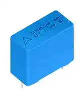


B32641H0153J189
Power Film Capacitor, Double Metallized PP, Radial Box - 2 Pin, 0.015 µF, ± 5%
- Manufacturer: TDK
- Product type: Power Film Capacitors
- ESR: -
- SVHC: No SVHC (25-Jun-2025)
- Capacitance: 0.015µF
- Voltage(AC): 600V
- Voltage(DC): 1kV
- Lead Spacing: 10mm
- Peak Current: -
- dv/dt Rating: 6.2kV/µs
- Output (kvar): -
- Product Range: B3264xH Series
- Product Width: 8mm
- Qualification: AEC-Q200
- Product Height: 17.5mm
- Product Length: 13mm
- Ripple Current: -
- Dielectric Type: Double Metallized PP
- Humidity Rating: GRADE III (Test Condition B)
- Product Diameter: -
- Capacitor Mounting: Through Hole
- RMS Current (Irms): -
- Capacitor Terminals: Radial Leaded
- Typical Applications: Ballast, High Frequency, LLC, SMPS
- Capacitance Tolerance: ± 5%
- Capacitor Case / Package: Radial Box - 2 Pin
- Operating Temperature Max: 125°C
- Operating Temperature Min: -55°C
| Delivery and price | |
|---|---|
| Units per pack | 3200 |
| Price | 0.486 € |
| Current stock | 10+ |
| Lead time | 30 days |
## **Film Capacitors**
Capacitors for Snubbering, Resonant Circuits, Power Factor Correction (PFC)
**Series/Type: B3264*H** Date: May 2025
TDK Electronics AG 2025. Reproduction, publication and dissemination of this publication, enclosures hereto and the information contained therein without TDK Electronics’ prior express consent is prohibited.
———E;_—xK—E”—>—E—ki—Ex—e **Film Capacitors B3264*H Capacitors for Snubbering, Resonant Circuits, Power Factor Correction (PFC)**
## **Typical Applications**
- Electronic ballasts (resonant circuits)
- LLC typology in resonant circuits
- High frequency applications with high current stress
- Switched-mode power supply
## **Climatic**
- Max. operating temperature: 125 °C (case)
- Climatic category (IEC 60068-1:2013): 55/110/56
## **Construction**
- Polypropylene (PP) dielectric with double sided metallized polyester (PET) film as electrodes
- Wound capacitor technology
- Plastic case (UL 94 V-0)
- Epoxy resin sealing
## **Features**
- Very compact design
- High pulse strength
- High current withstand capability
- Usable in harsh humidity environment
- Halogen free available on request
- AEC-Q200 compliant
## **Terminals**
- Parallel wire leads, lead-free tinned
- Special lead lengths available on request
## **Marking**
- Manufacturer’s logo
- Lot number, series number
- Rated capacitance (coded)
- Capacitance Tolerance (code letter)
- Rated DC voltage
- Date of manufacture (coded)
## **Delivery mode**
- Bulk (untaped)
- Taped (Ammo pack or reel)
- For notes on taping, refer to chapter “Taping and packing”
**2** a
Please read _Cautions and warnings_ and _Important notes_ at the end of this document.
**2** 5/25
**Film Capacitors**
**B3264*H**
**Capacitors for Snubbering, Resonant Circuits, Power Factor Correction (PFC)**
## **Dimensional drawing**
**==> picture [50 x 66] intentionally omitted <==**
## Dimensions in mm
## **Dimensions and types**
|Lead spacing<br>±0.4<br>_e_|Lead diameter<br>d1±0.05|Type|
|---|---|---|
|10|0.6|B32641H|
|15|0.8|B32642H|
|22.5|0.8|B32643H|
Please read _Cautions and warnings_ and _Important notes_ at the end of this document.
5/25
**3**
**Film Capacitors Capacitors for Snubbering, Resonant Circuits, Power Factor Correction (PFC)**
**B3264*H**
## **Overview of available types**
|Lead spacing|10 mm|10 mm|15 mm|15 mm|15 mm|15 mm|22.5 mm|22.5 mm|22.5 mm|22.5 mm|
|---|---|---|---|---|---|---|---|---|---|---|
|Type|B32641H||B32642H||||B32643H||||
|VR(V DC)|630|1000|630|1000|1600|2000|630|1000|1600|2000|
|VRMS(V AC)|400|600|400|600|650|700|400|600|650|700|
|CR(nF)|||||||||||
|2.2|||||||||||
|3.3|||||||||||
|3.9|||||||||||
|4.7|||||||||||
|5.6|||||||||||
|6.8|||||||||||
|8.2|||||||||||
|10|||||||||||
|12|||||||||||
|15|||||||||||
|18|||||||||||
|22|||||||||||
|27|||||||||||
|33|||||||||||
|39|||||||||||
|47|||||||||||
|56|||||||||||
|68|||||||||||
|82|||||||||||
|100|||||||||||
|120|||||||||||
|150|||||||||||
|220|||||||||||
|330|||||||||||
|390|||||||||||
|470|||||||||||
Please read _Cautions and warnings_ and _Important notes_ at the end of this document.
**4** 5/25
**Film Capacitors**
**B3264*H**
**Capacitors for Snubbering, Resonant Circuits, Power Factor Correction (PFC)**
## **Ordering codes and packing units B32641H (lead spacing 10 mm)**
|CR1)<br>nF|Max. dimensions<br>w x h x l<br>mm|Ordering code<br>(composition see<br>below)|Ammo pack<br>pcs./MOQ|Reel<br>pcs./MOQ|Untaped<br>pcs./MOQ|
|---|---|---|---|---|---|
|VR, DC= 630 V DC; VRMS(f ≤ 1 kHz) VR, AC= 400 V AC||||||
|6.8<br>8.2<br>10<br>12<br>15<br>18<br>22<br>27<br>33<br>39<br>47|4.0 x 9.0 x 13.0<br>4.0 x 9.0 x 13.0<br>5.0 x 11.0 x 13.0<br>5.0 x 11.0 x 13.0<br>5.0 x 11.0 x 13.0<br>5.0 x 11.0 x 13.0<br>6.0 x 12.0 x 13.0<br>6.0 x 12.0 x 13.0<br>6.0 x 14.0 x 13.0<br>7.0 x 16.0 x 13.0<br>8.0 x 17.5 x 13.0|B32641H6682+***<br>B32641H6822+***<br>B32641H6103+***<br>B32641H6123+***<br>B32641H6153+***<br>B32641H6183+***<br>B32641H6223+***<br>B32641H6273+***<br>B32641H6333+***<br>B32641H6393+***<br>B32641H6473+***|4000<br>4000<br>3320<br>3320<br>3320<br>3320<br>2720<br>2720<br>2720<br>3360<br>2960|6800<br>6800<br>5200<br>5200<br>5200<br>5200<br>4400<br>4400<br>4400<br>3600<br>3200|4000<br>4000<br>4000<br>4000<br>4000<br>4000<br>4000<br>4000<br>4000<br>4000<br>2000|
|VR, DC= 1000 V DC; VRMS(f ≤ 1 kHz) VR, AC= 600 V AC||||||
|2.2<br>3.3<br>3.9<br>4.7<br>5.6<br>6.8<br>8.2<br>10<br>12<br>15<br>18|4.0 x 9.0 x 13.0<br>5.0 x 11.0 x 13.0<br>5.0 x 11.0 x 13.0<br>5.0 x 11.0 x 13.0<br>6.0 x 12.0 x 13.0<br>6.0 x 12.0 x 13.0<br>6.0 x 14.0 x 13.0<br>6.0 x 14.0 x 13.0<br>7.0 x 16.0 x 13.0<br>8.0 x 17.5 x 13.0<br>8.0 x 17.5 x 13.0|B32641H0222+***<br>B32641H0332+***<br>B32641H0392+***<br>B32641H0472+***<br>B32641H0562+***<br>B32641H0682+***<br>B32641H0822+***<br>B32641H0103+***<br>B32641H0123+***<br>B32641H0153+***<br>B32641H0183+***|4000<br>3320<br>3320<br>3320<br>2720<br>2720<br>2720<br>2720<br>3360<br>2960<br>2960|6800<br>5200<br>5200<br>5200<br>4400<br>4400<br>4400<br>4400<br>3600<br>3200<br>3200|4000<br>4000<br>4000<br>4000<br>4000<br>4000<br>4000<br>4000<br>4000<br>2000<br>2000|
MOQ = Minimum Order Quantity, consisting of 4 packing units. Intermediate capacitance values on request.
## **Composition of ordering code**
- + = Capacitance tolerance code: J = ±5% K = ±10%
*** = Packaging code:
- 289 = Straight terminals, Ammo pack
189 = Straight terminals, Reel
000 = Straight terminals, Untaped (lead length 6 – 1 mm)
003 = Straight terminals, Untaped (lead length 3.2 ± 0.3 mm)
- (1) Capacitance value measured at 1 kHz
Please read _Cautions and warnings_ and _Important notes_ at the end of this document.
5/25
**5**
**Film Capacitors Capacitors for Snubbering, Resonant Circuits, Power Factor Correction (PFC)**
**B3264*H**
## **Ordering codes and packing units B32642H (lead spacing 15 mm)**
|CR1)<br>nF|Max. dimensions<br>w x h x l<br>mm|Ordering code<br>(composition see<br>below)|Ammo pack<br>pcs./MOQ|Reel<br>pcs./MOQ|Untaped<br>pcs./MOQ|
|---|---|---|---|---|---|
|VR, DC= 630 V DC; VRMS(f ≤ 1 kHz) VR, AC= 400 V AC||||||
|15<br>18<br>22<br>27<br>33<br>39<br>47<br>56<br>68<br>82<br>100<br>120<br>150|5.0 x 10.5 x 18.0<br>5.0 x 10.5 x 18.0<br>5.0 x 10.5 x 18.0<br>5.0 x 10.5 x 18.0<br>6.0 x 11.0 x 18.0<br>6.0 x 11.0 x 18.0<br>6.0 x 12.0 x 18.0<br>7.0 x 12.5 x 18.0<br>8.0 x 14.0 x 18.0<br>8.5 x 14.5 x 18.0<br>8.5 x 14.5 x 18.0<br>9.0 x 17.5 x 18.0<br>11.0 x 18.5 x 18.0|B32642H6153+***<br>B32642H6183+***<br>B32642H6223+***<br>B32642H6273+***<br>B32642H6333+***<br>B32642H6393+***<br>B32642H6473+***<br>B32642H6563+***<br>B32642H6683+***<br>B32642H6823+***<br>B32642H6104+***<br>B32642H6124+***<br>B32642H6154+***|4680<br>4680<br>4680<br>4680<br>3840<br>3840<br>3840<br>3320<br>2920<br>2720<br>2720<br>2560<br>2120|5200<br>5200<br>5200<br>5200<br>4400<br>4400<br>4400<br>3600<br>3000<br>2800<br>2800<br>2800<br>2200|4000<br>4000<br>4000<br>4000<br>4000<br>4000<br>4000<br>4000<br>2000<br>2000<br>2000<br>2000<br>1200|
MOQ = Minimum Order Quantity, consisting of 4 packing units. Intermediate capacitance values on request.
## **Composition of ordering code**
- + = Capacitance tolerance code: J = ±5% K = ±10%
- *** = Packaging code:
289 = Straight terminals, Ammo pack 189 = Straight terminals, Reel
000 = Straight terminals, Untaped (lead length 6 – 1 mm)
003 = Straight terminals, Untaped (lead length 3.2 ± 0.3 mm)
- (1) Capacitance value measured at 1 kHz
Please read _Cautions and warnings_ and _Important notes_ at the end of this document.
5/25
**6**
**Film Capacitors Capacitors for Snubbering, Resonant Circuits, Power Factor Correction (PFC)**
**B3264*H**
## **Ordering codes and packing units B32642H (lead spacing 15 mm)**
|CR1)<br>nF|Max. dimensions<br>w x h x l<br>mm|Ordering code<br>(composition see<br>below)|Ammo pack<br>pcs./MOQ|Reel<br>pcs./MOQ|Untaped<br>pcs./MOQ|
|---|---|---|---|---|---|
|VR, DC= 1000 V DC; VRMS(f ≤ 1 kHz) VR, AC= 600 V AC||||||
|10<br>12<br>15<br>18<br>22<br>27<br>33<br>39<br>47<br>56<br>68<br>82<br>100|5.0 x 10.5 x 18.0<br>5.0 x 10.5 x 18.0<br>5.0 x 10.5 x 18.0<br>6.0 x 11.0 x 18.0<br>6.0 x 12.0 x 18.0<br>7.0 x 12.5 x 18.0<br>7.0 x 12.5 x 18.0<br>8.0 x 14.0 x 18.0<br>8.5 x 14.5 x 18.0<br>9.0 x 17.5 x 18.0<br>9.0 x 17.5 x 18.0<br>11.0 x 18.5 x 18.0<br>11.0 x 18.5 x 18.0|B32642H0103+***<br>B32642H0123+***<br>B32642H0153+***<br>B32642H0183+***<br>B32642H0223+***<br>B32642H0273+***<br>B32642H0333+***<br>B32642H0393+***<br>B32642H0473+***<br>B32642H0563+***<br>B32642H0683+***<br>B32642H0823+***<br>B32642H0104K***|4680<br>4680<br>4680<br>3840<br>3840<br>3320<br>3320<br>2920<br>2720<br>2560<br>2560<br>2120<br>2120|5200<br>5200<br>5200<br>4400<br>4400<br>3600<br>3600<br>3000<br>2800<br>2800<br>2800<br>2200<br>2200|4000<br>4000<br>4000<br>4000<br>4000<br>4000<br>4000<br>2000<br>2000<br>2000<br>2000<br>1200<br>1200|
MOQ = Minimum Order Quantity, consisting of 4 packing units. Intermediate capacitance values on request.
## **Composition of ordering code**
- + = Capacitance tolerance code: J = ±5% K = ±10%
- *** = Packaging code:
- 289 = Straight terminals, Ammo pack 189 = Straight terminals, Reel
000 = Straight terminals, Untaped (lead length 6 – 1 mm)
003 = Straight terminals, Untaped (lead length 3.2 ± 0.3 mm)
- (1) Capacitance value measured at 1 kHz
Please read _Cautions and warnings_ and _Important notes_ at the end of this document.
5/25
**7**
**Film Capacitors Capacitors for Snubbering, Resonant Circuits, Power Factor Correction (PFC)**
**B3264*H**
## **Ordering codes and packing units B32642H (lead spacing 15 mm)**
|CR1)<br>nF|Max. dimensions<br>w x h x l<br>mm|Ordering code<br>(composition see<br>below)|Ammo pack<br>pcs./MOQ|Reel<br>pcs./MOQ|Untaped<br>pcs./MOQ|
|---|---|---|---|---|---|
|VR, DC= 1600 V DC; VRMS(f ≤ 1 kHz) VR, AC= 650 V AC||||||
|4.7<br>5.6<br>6.8<br>8.2<br>10<br>12<br>15<br>18<br>22<br>27<br>33<br>39<br>47<br>56|5.0 x 10.5 x 18.0<br>5.0 x 10.5 x 18.0<br>5.0 x 10.5 x 18.0<br>5.0 x 10.5 x 18.0<br>6.0 x 11.0 x 18.0<br>6.0 x 11.0 x 18.0<br>6.0 x 12.0 x 18.0<br>7.0 x 12.5 x 18.0<br>7.0 x 12.5 x 18.0<br>8.5 x 14.5 x 18.0<br>9.0 x 17.5 x 18.0<br>9.0 x 17.5 x 18.0<br>11.0 x 18.5 x 18.0<br>11.0 x 18.5 x 18.0|B32642H1472+***<br>B32642H1562+***<br>B32642H1682+***<br>B32642H1822+***<br>B32642H1103+***<br>B32642H1123+***<br>B32642H1153+***<br>B32642H1183+***<br>B32642H1223+***<br>B32642H1273+***<br>B32642H1333+***<br>B32642H1393+***<br>B32642H1473+***<br>B32642H1563+***|4680<br>4680<br>4680<br>4680<br>3840<br>3840<br>3840<br>3320<br>3320<br>2720<br>2560<br>2560<br>2560<br>2120|5200<br>5200<br>5200<br>5200<br>4400<br>4400<br>4400<br>3600<br>3600<br>2800<br>2800<br>2800<br>2800<br>2200|4000<br>4000<br>4000<br>4000<br>4000<br>4000<br>4000<br>4000<br>4000<br>2000<br>2000<br>2000<br>2000<br>1200|
MOQ = Minimum Order Quantity, consisting of 4 packing units. Intermediate capacitance values on request.
## **Composition of ordering code**
- + = Capacitance tolerance code: J = ±5% K = ±10%
*** = Packaging code:
- 289 = Straight terminals, Ammo pack
189 = Straight terminals, Reel
000 = Straight terminals, Untaped (lead length 6 – 1 mm)
003 = Straight terminals, Untaped (lead length 3.2 ± 0.3 mm)
- (1) Capacitance value measured at 1 kHz
Please read _Cautions and warnings_ and _Important notes_ at the end of this document.
5/25
**8**
**Film Capacitors Capacitors for Snubbering, Resonant Circuits, Power Factor Correction (PFC)**
**B3264*H**
## **Ordering codes and packing units B32642H (lead spacing 15 mm)**
|CR1)<br>nF|Max. dimensions<br>w x h x l<br>mm|Ordering code<br>(composition see<br>below)|Ammo pack<br>pcs./MOQ|Reel<br>pcs./MOQ|Untaped<br>pcs./MOQ|
|---|---|---|---|---|---|
|VR, DC= 2000 V DC; VRMS(f ≤ 1 kHz) VR, AC= 700 V AC||||||
|3.3<br>3.9<br>4.7<br>5.6<br>6.8<br>8.2<br>10<br>12<br>15<br>18<br>22<br>27|5.0 x 10.5 x 18.0<br>5.0 x 10.5 x 18.0<br>5.0 x 10.5 x 18.0<br>6.0 x 11.0 x 18.0<br>6.0 x 12.0 x 18.0<br>7.0 x 12.5 x 18.0<br>7.0 x 12.5 x 18.0<br>8.0 x 14.0 x 18.0<br>8.5 x 14.5 x 18.0<br>9.0 x 17.5 x 18.0<br>9.0 x 17.5 x 18.0<br>11.0 x 18.5 x 18.0|B32642H8332+***<br>B32642H8392+***<br>B32642H8472+***<br>B32642H8562+***<br>B32642H8682+***<br>B32642H8822+***<br>B32642H8103+***<br>B32642H8123+***<br>B32642H8153+***<br>B32642H8183+***<br>B32642H8223+***<br>B32642H8273+***|4680<br>4680<br>4680<br>3840<br>3840<br>3320<br>3320<br>2920<br>2720<br>2560<br>2560<br>2120|5200<br>5200<br>5200<br>4400<br>4400<br>3600<br>3600<br>3000<br>2800<br>2800<br>2800<br>2200|4000<br>4000<br>4000<br>4000<br>4000<br>4000<br>4000<br>2000<br>2000<br>2000<br>2000<br>1200|
MOQ = Minimum Order Quantity, consisting of 4 packing units. Intermediate capacitance values on request.
## **Composition of ordering code**
+ = Capacitance tolerance code: J = ±5% K = ±10%
*** = Packaging code: 289 = Straight terminals, Ammo pack 189 = Straight terminals, Reel
000 = Straight terminals, Untaped (lead length 6 – 1 mm) 003 = Straight terminals, Untaped (lead length 3.2 ± 0.3 mm)
- (1) Capacitance value measured at 1 kHz
Please read _Cautions and warnings_ and _Important notes_ at the end of this document.
5/25
**9**
**Film Capacitors**
**B3264*H**
**Capacitors for Snubbering, Resonant Circuits, Power Factor Correction (PFC)**
## **Ordering codes and packing units B32643H (lead spacing 22.5 mm)**
|CR1)<br>nF|Max. dimensions<br>w x h x l<br>mm|Ordering code<br>(composition see<br>below)|Ammo pack<br>pcs./MOQ|Reel<br>pcs./MOQ|Untaped<br>pcs./MOQ|
|---|---|---|---|---|---|
|VR, DC= 630 V DC; VRMS(f ≤ 1 kHz) VR, AC= 400 V AC||||||
|68<br>82<br>100<br>120<br>150<br>220<br>330<br>390<br>470|6.0 x 15.0 x 26.5<br>6.0 x 15.0 x 26.5<br>6.0 x 15.0 x 26.5<br>7.0 x 16.0 x 26.5<br>8.5 x 16.5 x 26.5<br>10.5 x 16.5 x 26.5<br>11.0 x 20.5 x 26.5<br>12.0 x 22.0 x 26.5<br>14.5 x 29.5 x 26.5|B32643H6683+***<br>B32643H6823+***<br>B32643H6104+***<br>B32643H6124+***<br>B32643H6154+***<br>B32643H6224+***<br>B32643H6334+***<br>B32643H6394+***<br>B32643H6474+***|2720<br>2720<br>2720<br>2320<br>1920<br>1560<br>1480<br>1320<br>-|2800<br>2800<br>2800<br>2400<br>2000<br>1600<br>1400<br>1200<br>-|2880<br>2880<br>2880<br>2520<br>2040<br>2160<br>2040<br>1800<br>1040|
MOQ = Minimum Order Quantity, consisting of 4 packing units. Intermediate capacitance values on request.
## **Composition of ordering code**
+ = Capacitance tolerance code: J = ±5% K = ±10%
*** = Packaging code:
289 = Straight terminals, Ammo pack 189 = Straight terminals, Reel
000 = Straight terminals, Untaped (lead length 6 – 1 mm)
003 = Straight terminals, Untaped (lead length 3.2 ± 0.3 mm)
- (1) Capacitance value measured at 1 kHz
Please read _Cautions and warnings_ and _Important notes_ at the end of this document.
5/25
**10**
**Film Capacitors Capacitors for Snubbering, Resonant Circuits, Power Factor Correction (PFC)**
**B3264*H**
## **Ordering codes and packing units B32643H (lead spacing 22.5 mm)**
|CR1)<br>nF|Max. dimensions<br>w x h x l<br>mm|Ordering code<br>(composition see<br>below)|Ammo pack<br>pcs./MOQ|Reel<br>pcs./MOQ|Untaped<br>pcs./MOQ|
|---|---|---|---|---|---|
|VR, DC= 1000 V DC; VRMS(f ≤ 1 kHz) VR, AC= 600 V AC||||||
|33<br>39<br>47<br>56<br>68<br>82<br>100<br>120<br>150<br>220<br>330<br>390|6.0 x 15.0 x 26.5<br>6.0 x 15.0 x 26.5<br>7.0 x 16.0 x 26.5<br>7.0 x 16.0 x 26.5<br>8.5 x 16.5 x 26.5<br>8.5 x 16.5 x 26.5<br>10.5 x 16.5 x 26.5<br>10.5 x 18.5 x 26.5<br>10.5 x 20.5 x 26.5<br>12.0 x 22.0 x 26.5<br>14.5 x 29.5 x 26.5<br>14.5 x 29.5 x 26.5|B32643H0333+***<br>B32643H0393+***<br>B32643H0473+***<br>B32643H0563+***<br>B32643H0683+***<br>B32643H0823+***<br>B32643H0104+***<br>B32643H0124+***<br>B32643H0154+***<br>B32643H0224+***<br>B32643H0334+***<br>B32643H0394+***|2720<br>2720<br>2320<br>2320<br>1920<br>1920<br>1560<br>1560<br>1560<br>1320<br>-<br>-|2800<br>2800<br>2400<br>2400<br>2000<br>2000<br>1600<br>1600<br>1600<br>1200<br>-<br>-|2880<br>2880<br>2520<br>2520<br>2040<br>2040<br>2160<br>2160<br>2160<br>1800<br>1040<br>1040|
MOQ = Minimum Order Quantity, consisting of 4 packing units. Intermediate capacitance values on request.
## **Composition of ordering code**
+ = Capacitance tolerance code: J = ±5% K = ±10%
*** = Packaging code: 289 = Straight terminals, Ammo pack 189 = Straight terminals, Reel 000 = Straight terminals, Untaped (lead length 6 – 1 mm) 003 = Straight terminals, Untaped (lead length 3.2 ± 0.3 mm)
- (1) Capacitance value measured at 1 kHz
Please read _Cautions and warnings_ and _Important notes_ at the end of this document.
5/25
**11**
**Film Capacitors Capacitors for Snubbering, Resonant Circuits, Power Factor Correction (PFC)**
**B3264*H**
## **Ordering codes and packing units B32643H (lead spacing 22.5 mm)**
|CR1)<br>nF|Max. dimensions<br>w x h x l<br>mm|Ordering code<br>(composition see<br>below)|Ammo pack<br>pcs./MOQ|Reel<br>pcs./MOQ|Untaped<br>pcs./MOQ|
|---|---|---|---|---|---|
|VR, DC= 1600 V DC; VRMS(f ≤ 1 kHz) VR, AC= 650 V AC||||||
|22<br>27<br>33<br>39<br>47<br>56<br>68<br>82<br>100<br>120<br>150<br>220|6.0 x 15.0 x 26.5<br>6.0 x 15.0 x 26.5<br>7.0 x 16.0 x 26.5<br>7.0 x 16.0 x 26.5<br>8.5 x 16.5 x 26.5<br>8.5 x 16.5 x 26.5<br>10.5 x 16.5 x 26.5<br>10.5 x 18.5 x 26.5<br>10.5 x 20.5 x 26.5<br>12.0 x 22.0 x 26.5<br>14.5 x 29.5 x 26.5<br>14.5 x 29.5 x 26.5|B32643H1223+***<br>B32643H1273+***<br>B32643H1333+***<br>B32643H1393+***<br>B32643H1473+***<br>B32643H1563+***<br>B32643H1683+***<br>B32643H1823+***<br>B32643H1104+***<br>B32643H1124+***<br>B32643H1154+***<br>B32643H1224+***|2720<br>2720<br>2320<br>2320<br>1920<br>1920<br>1560<br>1560<br>1560<br>1320<br>-<br>-|2800<br>2800<br>2400<br>2400<br>2000<br>2000<br>1600<br>1600<br>1600<br>1200<br>-<br>-|2880<br>2880<br>2520<br>2520<br>2040<br>2040<br>2160<br>2160<br>2160<br>1800<br>1040<br>1040|
MOQ = Minimum Order Quantity, consisting of 4 packing units. Intermediate capacitance values on request.
## **Composition of ordering code**
+ = Capacitance tolerance code: J = ±5% K = ±10%
*** = Packaging code:
289 = Straight terminals, Ammo pack 189 = Straight terminals, Reel
000 = Straight terminals, Untaped (lead length 6 – 1 mm) 003 = Straight terminals, Untaped (lead length 3.2 ± 0.3 mm)
- (1) Capacitance value measured at 1 kHz
Please read _Cautions and warnings_ and _Important notes_ at the end of this document.
5/25
**12**
**Film Capacitors**
**B3264*H**
**Capacitors for Snubbering, Resonant Circuits, Power Factor Correction (PFC)**
## **Ordering codes and packing units B32643H (lead spacing 22.5 mm)**
|CR1)<br>nF|Max. dimensions<br>w x h x l<br>mm|Ordering code<br>(composition see<br>below)|Ammo pack<br>pcs./MOQ|Reel<br>pcs./MOQ|Untaped<br>pcs./MOQ|
|---|---|---|---|---|---|
|VR, DC= 2000 V DC; VRMS(f ≤ 1 kHz) VR, AC= 700 V AC||||||
|10<br>12<br>15<br>18<br>22<br>27<br>33<br>39<br>47<br>56<br>68<br>82<br>100<br>120|6.0 x 15.0 x 26.5<br>6.0 x 15.0 x 26.5<br>6.0 x 15.0 x 26.5<br>7.0 x 16.0 x 26.5<br>7.0 x 16.0 x 26.5<br>8.5 x 16.5 x 26.5<br>8.5 x 16.5 x 26.5<br>10.5 x 16.5 x 26.5<br>10.5 x 18.5 x 26.5<br>11.0 x 20.5 x 26.5<br>12.0 x 22.0 x 26.5<br>12.0 x 22.0 x 26.5<br>14.5 x 29.5 x 26.5<br>14.5 x 29.5 x 26.5|B32643H8103+***<br>B32643H8123+***<br>B32643H8153+***<br>B32643H8183+***<br>B32643H8223+***<br>B32643H8273+***<br>B32643H8333+***<br>B32643H8393+***<br>B32643H8473+***<br>B32643H8563+***<br>B32643H8683+***<br>B32643H8823+***<br>B32643H8104+***<br>B32643H8124+***|2720<br>2720<br>2720<br>2320<br>2320<br>1920<br>1920<br>1560<br>1560<br>1480<br>1320<br>1320<br>-<br>-|2800<br>2800<br>2800<br>2400<br>2400<br>2000<br>2000<br>1600<br>1600<br>1400<br>1200<br>1200<br>-<br>-|2880<br>2880<br>2880<br>2520<br>2520<br>2040<br>2040<br>2160<br>2160<br>2040<br>1800<br>1800<br>1040<br>1040|
MOQ = Minimum Order Quantity, consisting of 4 packing units. Intermediate capacitance values on request.
## **Composition of ordering code**
- + = Capacitance tolerance code: J = ±5% K = ±10%
*** = Packaging code:
289 = Straight terminals, Ammo pack
189 = Straight terminals, Reel
000 = Straight terminals, Untaped (lead length 6 – 1 mm)
003 = Straight terminals, Untaped (lead length 3.2 ± 0.3 mm)
- (1) Capacitance value measured at 1 kHz
Please read _Cautions and warnings_ and _Important notes_ at the end of this document.
5/25
**13**
**Film Capacitors**
**B3264*H**
**Capacitors for Snubbering, Resonant Circuits, Power Factor Correction (PFC)**
## **Technical data**
Reference standard: IEC60384-16: 2019 and AEC-Q200D. All data given at T = 20 °C, unless otherwise specified
|specified|||||
|---|---|---|---|---|
|Rated temperature TR|+105 °C||||
|Operation temperature range|Max. operating temperature Top,max<br>+125 °C1)<br>Upper category temperature Tmax<br>+110 °C<br>Lower category temperature Tmin<br>–55 °C<br>Rated temperature TR<br>+105 °C||||
|Dissipation factor tan δ (in 10-3)<br>at 20 °C (upper limit values)|Frequency|C ≤ 0.1 uF|C > 0.1 uF||
||1 kHz<br>100 kHz|0.3<br>1.0|0.3<br>/||
|Insulation resistance Rins<br>at 20 °C,<br>rel. humidity ≤ 65%<br>(minimum as delivered values)|CR≤ 0.33 µF; 100 GΩ<br>CR˃ 0.33 µF; 30000 S||||
|Test voltage (terminal to terminal)|1.6 · VR, 2s||||
|Test voltage (terminal to case)|2000 V AC, 60s||||
|Peak current Ip(A)|C (µF) x dV/dt||||
|VR,DCat 105 °C|630 V DC|1000 V DC|1600 V DC|2000 V DC|
|VR,ACat 105 °C, f ≤ 1 kHz|400 V AC|600 V AC|650 V AC|700 V AC|
|Continuous operating voltage Vop<br>For temperature 105 °C < T ≤ 125 °C<br>(continuous operation with VDCor<br>VACat f ≤ 1 kHz)|1.25%/°C of Vopderating compared to Vopat 105 °C||||
|Reliability<br>Failure rate λ<br>Service life tSL|1 fit (≤ 1 · 10-9/h) at 0.5 · VR,DC, 40 °C<br>200000 h at 1.0· VR,DCand 85 °C<br>For conversion to other operating conditions and temperatures, refer<br>to chapter “Quality, 2 Reliability”.||||
1)Temperature given as operating Top (ambient temperature + self-heating), for example when ambient temperature is 125 °C, selfheating is 0 °C, or ripple current cannot be permitted.
Please read _Cautions and warnings_ and _Important notes_ at the end of this document.
5/25
**14**
**Film Capacitors**
**B3264*H**
**Capacitors for Snubbering, Resonant Circuits, Power Factor Correction (PFC)**
## **Pulse handling capability**
“dV/dt” represents the maximum permissible voltage change per unit of time for non-sinusoidal voltage, expressed in V/us.
“k0” represents the maximum permissible pulse characteristic of the waveform applied to the capacitor, expressed in V²/us
## Note:
The values of dV/dt and k0 provided below must not be exceeded in order to avoid damaging the capacitor. These parameters are given for isolated pulses in such a way that the heat generated by one pulse will be completely dissipated before applying the next pulse. For a train of pulses, please refer to the curves of permissible AC voltage-current versus frequency.
## **dV/dt values**
|**dV/dt values**|**dV/dt values**||||
|---|---|---|---|---|
|Lead spacing||10 mm|15 mm|22.5 mm|
|VR<br>V DC|VRMS<br>V AC|dV/dt in V/µs|||
|630|400|4000|2700|1500|
|1000|600|6200|3500|2100|
|1600|650|---|5300|3000|
|2000|700|---|6500|3800|
## **K0 values**
|**K0 values**|**K0 values**||||
|---|---|---|---|---|
|Lead spacing||10 mm|15 mm|22.5 mm|
|VR<br>V DC|VRMS<br>V AC|K0in V2/µs|||
|630|400|5 040 000|3 402 000|1 890 000|
|1000|600|12 400 000|7 000 000|4 200 000|
|1600|650|---|16 960 000|9 600 000|
|2000|700|---|26 000 000|15 000 000|
Please read _Cautions and warnings_ and _Important notes_ at the end of this document.
5/25
**15**
**B3264*H**
**Film Capacitors Capacitors for Snubbering, Resonant Circuits, Power Factor Correction (PFC)**
## **Impedance Z versus frequency** (typical values)
Please read _Cautions and warnings_ and _Important notes_ at the end of this document.
5/25
**16**
**Film Capacitors**
**B3264*H**
**Capacitors for Snubbering, Resonant Circuits, Power Factor Correction (PFC)**
**Permissible current IRMS versus frequency f (for sinusoidal waveforms, ambient temperature TA ≤85 °C, ΔT ≤15 °C)**
For TA >85 °C, please use derating factor FT.
Lead space 10 mm 630 V DC / 400 V AC
1000 V DC / 600 V AC
## Lead space 15 mm
630 V DC / 400 V AC
## 1000 V DC / 600 V AC
## Lead space 15 mm
1600 V DC / 650 V AC
## 2000 V DC / 700 V AC
Please read _Cautions and warnings_ and _Important notes_ at the end of this document.
5/25
**17**
**Film Capacitors**
**B3264*H**
**Capacitors for Snubbering, Resonant Circuits, Power Factor Correction (PFC)**
## Lead space 22.5 mm
## 630 V DC / 400 V AC
## Lead space 22.5 mm 1600 V DC / 650 V AC
## 1000 V DC / 600 V AC
## 2000 V DC / 700 V AC
Please read _Cautions and warnings_ and _Important notes_ at the end of this document.
5/25
**18**
**Film Capacitors**
**B3264*H**
**Capacitors for Snubbering, Resonant Circuits, Power Factor Correction (PFC)**
**Permissible AC voltage VRMS versus frequency f (for sinusoidal waveforms, ambient temperature TA ≤85 °C, ΔT ≤15 °C)**
For TA >85 °C, please use derating factor FT.
Lead space 10 mm
630 V DC / 400 V AC
1000 V DC / 600 V AC
## Lead space 15 mm
630 V DC / 400 V AC
## 1000 V DC / 600 V AC
## Lead space 15 mm
## 1600 V DC / 650 V AC
## 2000 V DC / 700 V AC
Please read _Cautions and warnings_ and _Important notes_ at the end of this document.
5/25
**19**
**Film Capacitors**
**B3264*H**
**Capacitors for Snubbering, Resonant Circuits, Power Factor Correction (PFC)**
## Lead space 22.5 mm
## 630 V DC / 400 V AC
## 1000 V DC / 600 V AC
## Lead space 22.5 mm
## 1600 V DC / 650 V AC
## 2000 V DC / 700 V AC
Please read _Cautions and warnings_ and _Important notes_ at the end of this document.
5/25
**20**
**Film Capacitors**
**B3264*H**
**Capacitors for Snubbering, Resonant Circuits, Power Factor Correction (PFC)**
## **Maximum AC voltage (VRMS), current (IRMS) versus frequency and temperature for TA >85 °C**
The graphs described in the previous section for the permissible AC voltage (VRMS) or current (IRMS) versus frequency are given for a maximum ambient temperature TA ≤85 °C.In case of higher ambient temperatures (TA), the self-heating (ΔT) of the component must be reduced to avoid that temperature of the component (Top = TA + ΔT) reaches values above maximum operating temperature. The factor FT shall be applied in the following way:
Derating factor for B3264xH
Maximum IRMS/VRMS as function of the ambient temperature: IRMS (TA) = IRMS,TA ≤85 °C · FT(TA) VRMS (TA) = VRMS,TA ≤85 °C · FT(TA)
Please read _Cautions and warnings_ and _Important notes_ at the end of this document.
5/25
**21**
**Film Capacitors**
**B3264*H**
**Capacitors for Snubbering, Resonant Circuits, Power Factor Correction (PFC)**
## **Maximum permissible DC voltage as a function of temperature (voltage derating)**
**==> picture [39 x 91] intentionally omitted <==**
**==> picture [181 x 37] intentionally omitted <==**
Please read _Cautions and warnings_ and _Important notes_ at the end of this document.
5/25
**22**
**Film Capacitors Film Capacitors**
**B3264*H**
## **Reliability Tests**
|Test<br>description|Reference|Test conditions|Failure criteria|Failure criteria|Failure criteria|Failure criteria|
|---|---|---|---|---|---|---|
||||Visible<br>damages||ΔC/C||tan δ<br>(1 kHz)|Rins|
|0 – Electricity<br>parameters|IEC 60384-16:2019|Capacitance: 1 kHz,1.0<br>V;<br>Loss factor: 1 kHz, 1.0 V;<br>100KHz, 1.0 V;<br>Voltage proof: 1.6 VR, 1<br>min;<br>Insulation Resistance:<br>500 V,1 min;|Yes|Out of specified<br>limits||Out of<br>specified<br>limits|
|1- Damp heat,<br>loading|IEC 60384-16:2019|40 °C/93% relative<br>humidity/VR,DC/56 days|Yes|> 5%|> 0.002|< 50% of<br>initial limit|
|2 –Damp heat,<br>loading|/|85 °C/85% relative<br>humidity/VR,DC/1000 hrs|Yes|> 10%|> 0.005|< 50% of<br>initial limit|
|3 –Damp heat,<br>loading|/|85 °C/85% relative<br>humidity/ VR,AC/1000 hrs|Yes|> 10%|> 0.005|< 50% of<br>initial limit|
|4 – Endurance|IEC 60384-16:2019|105 °C/1.25*VR,DC/1000<br>hrs|Yes|> 5%|> 0.004|< 50% of<br>initial limit|
|5 – Rapid<br>Change of<br>temperature|IEC 60384-16:2019|TA= Lower category<br>temperature<br>TB= Upper category<br>temperature<br>Five cycles<br>Duration t = 30 min|Yes|> 2%|> 0.002|< 50% of<br>initial limit|
|6 - Vibration|IEC 60384-16:2019|Test: vibration sinusoidal<br>Displacement: 0.75 mm<br>Accleration: 100 m/s2<br>Whichever is the lower<br>amplitude<br>Frequency: 10 Hz ... 500<br>Hz<br>Test duration: 3<br>orthogonal axes,<br>2 hours each axe|Yes|-|-|-|
|7 – Bump|IEC 60384-16:2019|Test: Total 4000 bumps<br>with<br>400 m/s2mounted on<br>PCB<br>Duration: 6 ms|Yes|> 2%|> 0.002|< 50% of<br>initial limit|
Please read _Cautions and warnings_ and _Important notes_ at the end of this document.
**23** 5/25
**Film Capacitors Film Capacitors**
**B3264*H**
|Test<br>description|Reference|Test conditions|Failure criteria|Failure criteria|Failure criteria|Failure criteria|
|---|---|---|---|---|---|---|
||||Visible<br>damages||ΔC/C||tan δ<br>(1 kHz)|Rins|
|8 – Climatic<br>sequence|IEC 60384-16:2019|Dry heat Tb / 16 h<br>Damp heat cyclic, 1st<br>cycle<br>+55 °C / 24 h / 95% ...<br>100% RH<br>Cold Ta / 2 h<br>Damp heat cyclic, 5<br>cycles<br>+55 °C / 24 h / 95% ...<br>100% RH|Yes|> 2%|> 0.002|< 50% of<br>initial limit|
|9 – Resistance<br>to soldering<br>heat|IEC 60068-2-20:2008|Solder bath at +260 °C ±<br>5 °C|Yes|> 2%|> 0.002|< 50% of<br>initial limit|
## **Construction MMKP**
**==> picture [202 x 186] intentionally omitted <==**
Dielectric film (1): Metallized polyethylene terephthalate (polyester, PET) Dielectric film (2): Polypropylene (PP) Dielectric film (3): Metallized Polypropylene (PP) Metal spray (4): Lead free alloy Sealing (5): Epoxy resin sealing Case (6): PBT, according to UL 94-0 Terminal (7): Lead free tinned wire
Please read _Cautions and warnings_ and _Important notes_ at the end of this document.
5/25
**24**
**Film Capacitors Film Capacitors**
**B3264*H**
## **Soldering**
## **Solderability of leads**
The solderability of terminal leads is tested to IEC 60068-2-20:2008, test Ta, method 1. Before a solderability test is carried out, terminals are subjected to accelerated ageing (to IEC 60068-22:2007, test Ba: 4 h exposure to dry heat at 155 °C). Since the ageing temperature is far higher than the upper category temperature of the capacitors, the terminal wires should be cut off from the capacitor before the ageing procedure to prevent the solderability being impaired by the products of any capacitor decomposition that might occur.
|Solder bath temperature|235 ± 5 °C|
|---|---|
|Solderingtime|2.0 ± 0.5 s|
|Immersion depth|2.0 +0/–0.5 mm from capacitor bodyor seating plane|
|Evaluation criteria:<br>Visual inspection|Wetting of wire surface by new solder90%,<br>free-flowingsolder|
## **Resistance to soldering heat**
Resistance to soldering heat is tested to IEC 60068-2-20:2008, test Tb, method 1. Conditions:
|Conditions:|||
|---|---|---|
|Series|Solder bath temperature|Soldering time|
|MKT<br>boxed (except 2.5 x 6.5 x7.2 mm)<br>coated<br>uncoated(lead spacing> 10 mm)|260 ± 5 °C|10 ± 1 s|
|MFP<br>MKP<br>(lead spacing> 7.5 mm)|||
|MKT<br>boxed(case 2.5 x 6.5 x 7.2 mm)||5 ± 1 s|
|MKP<br>(lead spacing7.5 mm)<br>MKT<br>uncoated (lead spacing10 mm)<br>insulated (B32559)||< 4 s recommended soldering<br>profile for MKT uncoated<br>(lead spacing10 mm) and<br>insulated(B32559)|
Please read _Cautions and warnings_ and _Important notes_ at the end of this document.
5/25
**25**
**Film Capacitors Film Capacitors**
**B3264*H**
|Immersion depth|2.0 +0/–0.5 mm from capacitor bodyor seating plane|
|---|---|
|Shield|Heat-absorbing board, (1.5 ± 0.5) mm thick, between<br>capacitor bodyand liquid solder|
|Evaluation criteria:<br>Visual inspection<br>C/C0<br>tan|No visible damage<br>2% for MKT/MKP/MFP<br>5% for EMI suppression capacitors<br>As specified in sectional specification|
## **General notes on soldering**
Permissible heat exposure loads on film capacitors are primarily characterized by the upper category temperature Tmax. Long exposure to temperatures above this type-related temperature limit can lead to changes in the plastic dielectric and thus change irreversibly a capacitor's electrical characteristics. For short exposures (as in practical soldering processes) the heat load (and thus the possible effects on a capacitor) will also depend on other factors like:
- Pre-heating temperature and time
- Forced cooling immediately after soldering
- Terminal characteristics: diameter, length, thermal resistance, special configurations (e.g. crimping)
- Height of capacitor above solder bath
- Shadowing by neighboring components
- Additional heating due to heat dissipation by neighboring components
- Use of solder-resist coatings
Please read _Cautions and warnings_ and _Important notes_ at the end of this document.
5/25
**26**
**Film Capacitors Film Capacitors**
**B3264*H**
The overheating associated with some of these factors can usually be reduced by suitable countermeasures. For example, if a pre-heating step cannot be avoided, an additional or reinforced cooling process may possibly have to be included.
## **TDK Recommendations**
As a reference, the recommended wave soldering profile for our film capacitors is as follows:
**==> picture [94 x 42] intentionally omitted <==**
**==> picture [294 x 175] intentionally omitted <==**
Please read _Cautions and warnings_ and _Important notes_ at the end of this document.
5/25
**27**
**Film Capacitors Film Capacitors**
**B3264*H**
Body temperature should follow the description below:
- MKP capacitor
> During pre-heating: Tp 110 °C
> During soldering: Ts 120 °C, ts 45 s
- MKT capacitor During pre-heating: Tp 125 °C
> During soldering: Ts 160 °C, ts 45 s
When SMD components are used together with leaded ones, the film capacitors should not pass into the SMD adhesive curing oven. The leaded components should be assembled after the SMD curing step. Leaded film capacitors are not suitable for reflow soldering.
In order to ensure proper conditions for manual or selective soldering, the body temperature of the capacitor (Ts) must be ≤120 °C.
One recommended condition for manual soldering is that the tip of the soldering iron should be <360 °C and the soldering contact time should be no longer than 3 seconds.
For uncoated MKT capacitors with lead spacings ≤10 mm (B32560/B32561) the following measures are recommended:
- pre-heating to not more than 110 °C in the preheater phase
- rapid cooling after soldering
## **Cleaning**
To determine whether the following solvents, often used to remove flux residues and other substances, are suitable for the capacitors described, refer to the table below:
|Type|Ethanol, isopropanol, n-propanol|n-propanol-water mixtures, water<br>with surface tension-reducing<br>tensides(neutral)|
|---|---|---|
|MKT(uncoated)|Suitable|Unsuitable|
|MKT, MKP, MFP<br>(coated/boxed)||Suitable|
Even when suitable solvents are used, a reversible change of the electrical characteristics may occur in uncoated capacitors immediately after they are washed. Thus it is always recommended to dry the components (e.g. 4 h at 70 °C) before they are subjected to subsequent electrical testing.
## **Caution:**
Consult us first if you wish to use new solvents!
## **Embedding of capacitors in finished assemblies**
In many applications, finished circuit assemblies are embedded in plastic resins. In this case, both chemical and thermal influences of the embedding ("potting") and curing processes must be taken into account. Our experience has shown that the following potting materials can be recommended: non-flexible epoxy resins with acid-anhydride hardeners; chemically inert, non-conducting fillers; maximum curing temperature of 100 °C.
## **Caution:**
Consult us first if you wish to embed uncoated types!
Please read _Cautions and warnings_ and _Important notes_ at the end of this document.
5/25
**28**
**Film Capacitors Film Capacitors**
**B3264*H**
## **Marking**
## **Capacitor markings**
Depending on the capacitor size, the markings are positioned either on the side and/or the top of the component. The coded forms specified in IEC 60062:2004 are used to indicate the rated capacitance, capacitance tolerance and date of manufacture.
The lot number (production batch number) ensures unique identification of a particular capacitor and allows, together with the date of manufacture, exact assignment to the process data of the entire production run (traceability).
|Marking example|Remarks|
|---|---|
||Manufacturer‘s logo<br>1st line:<br>Lot number<br>(1 character, 9 digits),<br>series number (film material is coded in the series<br>number)<br>2nd line:<br>CR, tolerance, VR,<br>date of manufacture (year and month coded)|
## **Codes for rated capacitance**
|**Codes for rated capacitance**|||
|---|---|---|
|Rated capacitance|To IEC 60062|Short code|
|100 pF|100p|n1|
|150 pF|150p|n15|
|1.0 nF|1n0|1n|
|1.5 nF|1n5||
|10 nF|10n||
|100 nF|100n|1|
|150 nF|150n|15|
|1.0F|1|1|
|1.5F|15||
|10F|1||
|15F|15||
Please read _Cautions and warnings_ and _Important notes_ at the end of this document.
5/25
**29**
**Film Capacitors Film Capacitors**
**B3264*H**
## **Codes for capacitance tolerance**
|Capacitance tolerance|Code letter|Remark|
|---|---|---|
||A|Capacitance tolerances for which no code letter is defined can be<br>indicated by an A.<br>The meaning of code A must then be mutually specified in other<br>documentation.|
|±2.5%|H||
|±5%|J||
|±10%|K||
|±20%|M||
## **Codes for date of manufacture (to IEC 60062:2004)**
|Code foryear|Code foryear|Code foryear|Code foryear|Code foryear|Code for month|Code for month|Code for month|Code for month|Code for month|
|---|---|---|---|---|---|---|---|---|---|
|Year|Code<br>letter||Year|Code<br>letter|Month|Code<br>numeral||Month|Code<br>numeral/letter|
|2023|R||2029|X|January|1||July|7|
|2024|S||2030|A|February|2||August|8|
|2025|T||2031|B|March|3||September|9|
|2026|U||2032|C|April|4||October|O|
|2027|V||2033|D|May|5||November|N|
|2028|W||2034|E|June|6||December|D|
E.g.: J5 2017 May
## **Marking types**
The capacitors may have either an ink-jet marking or a laser marking. The main advantage of laser marking is that it cannot be removed by solvents, which ensures the reliable identification of the capacitor. Moreover, because the laser marking process reduces the amount of chemicals used, it is an environmentally friendly marking solution.
Please read _Cautions and warnings_ and _Important notes_ at the end of this document.
5/25
**30**
**Film Capacitors Film Capacitors**
**B3264*H**
## **Ordering code system**
A component and the packing in which it is to be delivered are defined by the ordering code, which has 15 digits (plus 3 additional digits for internal use). For all capacitors the ordering codes are explicitly stated (together with the corresponding tolerance and/or packing variants) in the data sheets.
Should there be any doubt about the coding system, however, then it is better to order the capacitor using a plain text description (i.e. without a code).
## **Basic structure of the ordering code:**
|Digit|1<br>2<br>3<br>4<br>5<br>6<br>7<br>8<br>9<br>10<br>11<br>12<br>13<br>14<br>15<br>16<br>17<br>18<br>**B**<br>Block 1<br>Block 2<br>Block 3<br>Block 4 (for<br>internal use)|1<br>2<br>3<br>4<br>5<br>6<br>7<br>8<br>9<br>10<br>11<br>12<br>13<br>14<br>15<br>16<br>17<br>18<br>**B**<br>Block 1<br>Block 2<br>Block 3<br>Block 4 (for<br>internal use)|1<br>2<br>3<br>4<br>5<br>6<br>7<br>8<br>9<br>10<br>11<br>12<br>13<br>14<br>15<br>16<br>17<br>18<br>**B**<br>Block 1<br>Block 2<br>Block 3<br>Block 4 (for<br>internal use)|1<br>2<br>3<br>4<br>5<br>6<br>7<br>8<br>9<br>10<br>11<br>12<br>13<br>14<br>15<br>16<br>17<br>18<br>**B**<br>Block 1<br>Block 2<br>Block 3<br>Block 4 (for<br>internal use)|1<br>2<br>3<br>4<br>5<br>6<br>7<br>8<br>9<br>10<br>11<br>12<br>13<br>14<br>15<br>16<br>17<br>18<br>**B**<br>Block 1<br>Block 2<br>Block 3<br>Block 4 (for<br>internal use)|1<br>2<br>3<br>4<br>5<br>6<br>7<br>8<br>9<br>10<br>11<br>12<br>13<br>14<br>15<br>16<br>17<br>18<br>**B**<br>Block 1<br>Block 2<br>Block 3<br>Block 4 (for<br>internal use)|1<br>2<br>3<br>4<br>5<br>6<br>7<br>8<br>9<br>10<br>11<br>12<br>13<br>14<br>15<br>16<br>17<br>18<br>**B**<br>Block 1<br>Block 2<br>Block 3<br>Block 4 (for<br>internal use)|1<br>2<br>3<br>4<br>5<br>6<br>7<br>8<br>9<br>10<br>11<br>12<br>13<br>14<br>15<br>16<br>17<br>18<br>**B**<br>Block 1<br>Block 2<br>Block 3<br>Block 4 (for<br>internal use)|1<br>2<br>3<br>4<br>5<br>6<br>7<br>8<br>9<br>10<br>11<br>12<br>13<br>14<br>15<br>16<br>17<br>18<br>**B**<br>Block 1<br>Block 2<br>Block 3<br>Block 4 (for<br>internal use)|
|---|---|---|---|---|---|---|---|---|---|
|Digit||Meaning||||||||
|1||B = Passive components||||||||
|2,3||32 = Metallized film capacitors, EMI suppression capacitors<br>81 = EMI suppression capacitors||||||||
|4 ... 6||Type (block 1 is termed the "type number")||||||||
|7||Revision status||||||||
|8||Rated DC voltage, coded (not for EMI suppression capacitors)||||||||
|9 ... 11||Rated capacitance (coding method for value in pF)<br>Examples:||||||||
|||Digit<br>B 3 2 6 4 2 H 6|9<br>10 11<br>1<br>5<br>4 K<br>=||||||15<br>• 10 4 pF = 150 nF|
||||1||5||4|||
|||||||||||
|||||||||||
|||||||||||
|12||Code letter for capacitance tolerance||||||||
|13 ... 15||Codes for lead and taping parameters (refer to respective data sheet)||||||||
|16 ... 18||Internal use||||||||
Please read _Cautions and warnings_ and _Important notes_ at the end of this document.
5/25
**31**
**Film Capacitors Film Capacitors**
**B3264*H**
## **Cautions and warnings**
- Do not exceed the upper category temperature (UCT).
- Do not apply any mechanical stress to the capacitor terminals.
- Avoid any compressive, tensile or flexural stress.
- Do not move the capacitor after it has been soldered to the PC board.
- Do not pick up the PC board by the soldered capacitor.
- Do not place the capacitor on a PC board whose PTH hole spacing differs from the specified lead spacing.
- Do not exceed the specified time or temperature limits during soldering.
- Avoid external energy inputs, such as fire or electricity.
- Avoid overload of the capacitors.
- Consult us if application is with severe temperature and humidity condition.
- There are no serviceable or repairable parts inside the capacitor. Opening the capacitor or any attempts to open or repair the capacitor will void the warranty and liability of TDK Electronics.
- Please note that the standards referred to in this publication may have been revised in the meantime.
The table below summarizes the safety instructions that must always be observed. A detailed description can be found in the relevant sections of the chapters "General technical information" and "Mounting guidelines".
|Topic|Safety information|Reference chapter<br>"General technical<br>information"|
|---|---|---|
|Storage conditions|Make sure that capacitors are stored within the spe-<br>cified range of time, temperature and humidity condi-<br>tions.|4.5 "Storage conditions"|
|Flammability|Avoid external energy, such as fire or electricity (pas-<br>sive flammability), avoid overload of the capacitors<br>(active flammability) and consider the flammability of<br>materials.|5.3 "Flammability"|
|Resistance to<br>vibration|Do not exceed the tested ability to withstand vibrati-<br>on.<br>The capacitors are tested to IEC 60068-2-6:2007.<br>TDK Electronics offers film capacitors specially de-<br>signed for operation under more severe vibration re-<br>gimes such as those found in automotive applicati-<br>ons. Consult our catalog "Film Capacitors for Auto-<br>motive Electronics".|5.2 "Resistance to vibration"|
|Soldering|Do not exceed the specified time or temperature li-<br>mits during soldering.|1 "Soldering"|
|Cleaning|Use only suitable solvents for cleaning capacitors.|2 "Cleaning"|
|Embedding of capaci-<br>tors in finished assem-<br>blies|When embedding finished circuit assemblies in plas-<br>tic resins, chemical and thermal influences must be<br>taken into account.<br>Caution: Consult us first, if you also wish to embed<br>other uncoated component types!|3 "Embedding of capacitors<br>in finished assemblies"|
**32** April
**Film Capacitors Film Capacitors**
**B3264*H**
## **Display of ordering codes for TDK Electronics products**
The ordering code for one and the same product can be represented differently in data sheets, data books, other publications, on the company website, or in order-related documents such as shipping notes, order confirmations and product labels. The varying representations of the ordering codes are due to different processes employed and do not affect the specifications of the respective products.
Detailed information can be found on the Internet under www.tdk-electronics.tdk.com/orderingcodes.
## **Correlation of data sheet values and modelling tool outputs**
Data sheet values and results of design tools may deviate as they have not been derived in the same context.
While data sheets show individual parameter statements without considering a possible dependency to other parameters. Tools model a complete given scenario as input and processed inside the tool. Furthermore as we constantly strive to improve our models, the results of tools can change over time and be a non-binding indication only.
**33**
April
**Film Capacitors**
**B3264*H**
**Capacitors for Snubbering, Resonant Circuits, Power Factor Correction (PFC)**
## **Symbols and terms**
|Symbol|English|German|
|---|---|---|
|<br>C<br>A<br>C<br>C<br>CR<br>C<br>C/C<br>C/CR<br>dt<br>t<br>T<br>tan<br>V<br>dV/dt<br>V/t<br>E<br>ESL<br>ESR<br>f<br>f1<br>f2<br>fr<br>FD<br>FT<br>i<br>IC<br>IRMS<br>iz<br>k0<br>LS<br>|Heat transfer coefficient<br>Temperature coefficient of capacitance<br>Capacitor surface area<br>Humidity coefficient of capacitance<br>Capacitance<br>Rated capacitance<br>Absolute capacitance change<br>Relative capacitance change<br>(relative deviation of actual value)<br>Capacitance tolerance<br>(relative deviation from rated capacitance)<br>Time differential<br>Time interval<br>Absolute temperature change<br>(self-heating)<br>Absolute change of dissipation factor<br>Absolute voltage change<br>Time differential of voltage function<br>(rate of voltage rise)<br>Voltage change per time interval<br>Activation energy for diffusion<br>Self-inductance<br>Equivalent series resistance<br>Frequency<br>Frequency limit for reducing permissible<br>AC voltage due to thermal limits<br>Frequency limit for reducing permissible<br>AC voltage due to current limit<br>Resonant frequency<br>Thermal acceleration factor for diffusion<br>Derating factor<br>Current (peak)<br>Category current (max. continuous current)<br>(Sinusoidal) alternating current, root-mean-<br>square value<br>Capacitance drift<br>Pulse characteristic<br>Series inductance<br>Failure rate|Wärmeübergangszahl<br>Temperaturkoeffizient der Kapazität<br>Kondensatoroberfläche<br>Feuchtekoeffizient der Kapazität<br>Kapazität<br>Nennkapazität<br>Absolute Kapazitätsänderung<br>Relative Kapazitätsänderung<br>(relative Abweichung vom Ist-Wert)<br>Kapazitätstoleranz<br>(relative Abweichung vom Nennwert)<br>Differentielle Zeit<br>Zeitintervall<br>Absolute Temperaturänderung<br>(Selbsterwärmung)<br>Absolute Änderung des Verlustfaktors<br>Absolute Spannungsänderung<br>Differentielle Spannungsänderung<br>(Spannungsflankensteilheit)<br>Spannungsänderung pro Zeitintervall<br>Aktivierungsenergie zur Diffusion<br>Eigeninduktivität<br>Ersatz-Serienwiderstand<br>Frequenz<br>Grenzfrequenz für thermisch bedingte<br>Reduzierung der zulässigen Wechselspannung<br>Grenzfrequenz für strombedingte Reduzierung der<br>zulässigen Wechselspannung<br>Resonanzfrequenz<br>Therm. Beschleunigungsfaktor zur Diffusion<br>Deratingfaktor<br>Stromspitze<br>Kategoriestrom (max. Dauerstrom)<br>(Sinusförmiger) Wechselstrom<br>Inkonstanz der Kapazität<br>Impulskennwert<br>Serieninduktivität<br>Ausfallrate|
Please read _Cautions and warnings_ and _Important notes_ at the end of this document.
**34** 5/25
**Film Capacitors Capacitors for Snubbering, Resonant Circuits, Power Factor Correction (PFC)**
**B3264*H**
|Symbol|English|German|
|---|---|---|
|0<br>test<br>Pdiss<br>Pgen<br>Q<br><br>R<br>R<br>Ri<br>Rins<br>RP<br>RS<br>S<br>t<br>T<br><br>tan<br>tanD<br>tanP<br>tanS<br>TA<br>Tmax<br>Tmin<br>tOL<br>Top<br>TR<br>Tref<br>tSL<br>VAC<br>VC<br>VC,RMS<br>VCD<br>Vch<br>VDC<br>VFB|Constant failure rate during useful service life <br>Failure rate, determined by tests<br>Dissipated power<br>Generated power<br>Heat energy<br>Density of water vapor in air<br>Universal molar constant for gases<br>Ohmic resistance of discharge circuit<br>Internal resistance<br>Insulation resistance<br>Parallel resistance<br>Series resistance<br>severity (humidity test)<br>Time<br>Temperature<br>Time constant<br>Dissipation factor<br>Dielectric component of dissipation factor<br>Parallel component of dissipation factor<br>Series component of dissipation factor<br>Temperature of the air surrounding the<br>component<br>Upper category temperature<br>Lower category temperature<br>Operating life at operating temperature and<br>voltage<br>Operating temperature, TA+T<br>Rated temperature<br>Reference temperature<br>Reference service life<br>AC voltage<br>Category voltage<br>Category AC voltage<br>Corona-discharge onset voltage<br>Charging voltage<br>DC voltage<br>Fly-back capacitor voltage|Konstante Ausfallrate in der Nutzungsphase<br>Experimentell ermittelte Ausfallrate<br>Abgegebene Verlustleistung<br>Erzeugte Verlustleistung<br>Wärmeenergie<br>Dichte von Wasserdampf in Luft<br>Allg. Molarkonstante für Gas<br>Ohmscher Widerstand des Entladekreises<br>Innenwiderstand<br>Isolationswiderstand<br>Parallelwiderstand<br>Serienwiderstand<br>Schärfegrad (Feuchtetest)<br>Zeit<br>Temperatur<br>Zeitkonstante<br>Verlustfaktor<br>Dielektrischer Anteil des Verlustfaktors<br>Parallelanteil des Verlfustfaktors<br>Serienanteil des Verlustfaktors<br>Temperatur der Luft, die das Bauteil umgibt<br>Obere Kategorietemperatur<br>Untere Kategorietemperatur<br>Betriebszeit bei Betriebstemperatur und<br>-spannung<br>Beriebstemperatur, TA+T<br>Nenntemperatur<br>Referenztemperatur<br>Referenz-Lebensdauer<br>Wechselspannung<br>Kategoriespannung<br>(Sinusförmige) Kategorie-Wechselspannung<br>Teilentlade-Einsatzspannung<br>Ladespannung<br>Gleichspannung<br>Spannung (Flyback)|
Please read _Cautions and warnings_ and _Important notes_ at the end of this document.
**35** 5/25
**Film Capacitors Capacitors for Snubbering, Resonant Circuits, Power Factor Correction (PFC)**
**B3264*H**
|Symbol|English|German|
|---|---|---|
|Vi<br>Vo<br>Vop<br>Vp<br>Vpp<br>VR<br>^VR<br>VRMS<br>VSC<br>Vsn<br>Z<br>~~_e_~~|Input voltage<br>Output voltage<br>Operating voltage<br>Peak pulse voltage<br>Peak-to-peak voltage Impedance<br>Rated voltage<br>Amplitude of rated AC voltage<br>(Sinusoidal) alternating voltage,<br>root-mean-square value<br>S-correction voltage<br>Snubber capacitor voltage<br>Impedance<br>Lead spacing|Eingangsspannung<br>Ausgangssspannung<br>Betriebsspannung<br>Impuls-Spitzenspannung<br>Spannungshub<br>Nennspannung<br>Amplitude der Nenn-Wechselspannung<br>(Sinusförmige) Wechselspannung<br>Spannung bei Anwendung "S-correction”<br>Spannung bei Anwendung "Beschaltung"<br>Scheinwiderstand<br>Rastermaß|
Please read _Cautions and warnings_ and _Important notes_ at the end of this document.
5/25
**36**
## **Important notes**
The following applies to all products named in this publication:
- 1 Some parts of this publication contain **statements about the suitability of our products for certain areas of application** . These statements are based on our knowledge of typical requirements that are often placed on our products in the areas of application concerned. We nevertheless expressly point out **that such statements cannot be regarded as binding statements about the suitability of our products for a particular customer application** . As a rule we are either unfamiliar with individual customer applications or less familiar with them than the customers themselves. For these reasons, it is always ultimately incumbent on the customer to check and decide whether a product with the properties described in the product specification is suitable for use in a particular customer application.
- 2 We also point out that **in individual cases, a malfunction of electronic components or failure before the end of their usual service life cannot be completely ruled out in the current state of the art, even if they are operated as specified** . In customer applications requiring a very high level of operational safety and especially in customer applications in which the malfunction or failure of an electronic component could endanger human life or health (e.g. in accident prevention or life-saving systems), it must therefore be ensured by means of suitable design of the customer application or other action taken by the customer (e.g. installation of protective circuitry or redundancy) that no injury or damage is sustained by third parties in the event of malfunction or failure of an electronic component.
- 3 **The warnings, cautions and product-specific notes must be observed** .
- 4 In order to satisfy certain technical requirements, **some of the products described in this publication may contain substances subject to restrictions in certain jurisdictions (e.g. because they are classed as hazardous)** . Useful information on this will be found in our Material Data Sheets on the Internet (www.tdk-electronics.tdk.com/material). Should you have any more detailed questions, please contact our sales offices.
- 5 We constantly strive to improve our products. Consequently, **the products described in this publication may change from time to time** . The same is true of the corresponding product specifications. Please check therefore to what extent product descriptions and specifications contained in this publication are still applicable before or when you place an order.
- We also **reserve the right to discontinue production and delivery of products** . Consequently, we cannot guarantee that all products named in this publication will always be available. The aforementioned does not apply in the case of individual agreements deviating from the foregoing for customer-specific products.
- 6 Unless otherwise agreed in individual contracts, **all orders are subject to our General Terms and Conditions of Supply** .
- 7 **Our manufacturing sites serving the automotive business apply the IATF 16949 standard** . The IATF certifications confirm our compliance with requirements regarding the quality management system in the automotive industry. Referring to customer requirements and customer specific requirements (“CSR”) TDK always has and will continue to have the policy of respecting individual agreements. Even if IATF 16949 may appear to support the acceptance of unilateral requirements, we hereby like to emphasize that **only requirements mutually agreed upon can and will be implemented in our Quality Management System** . For clarification purposes we like to point out that obligations from IATF 16949 shall only become legally binding if individually agreed upon.
**37** 5/25
## **Important notes**
- 8 The trade names EPCOS, CarXield, CeraCharge, CeraDiode, CeraLink, CeraPad, CeraPlas, CSMP, CTVS, DeltaCap, DigiSiMic, FilterCap, FormFit, InsuGate, LeaXield, MediPlas, MiniBlue, MiniCell, MKD, MKK, ModCap, MotorCap, PCC, PhaseCap, PhaseCube, PhaseMod, PhiCap, PiezoBrush, PlasmaBrush, PowerHap, PQSine, PQvar, SIFERRIT, SIFI, SIKOREL, SilverCap, SIMDAD, SiMic, SIMID, SineFormer, SIOV, SurfIND, ThermoFuse, WindCap, XieldCap are **trademarks registered or pending** in Europe and in other countries. Further information will be found on the Internet at www.tdkelectronics.tdk.com/trademarks.
## Release 2024-02
5/25
**38**
Updated at April 27, 2026
TDK Corporation is a globally recognized leader in electronic components and magnetic materials. Founded in 1935 to commercialize ferrites, the Tokyo-based company has evolved into a comprehensive manufacturer of high-performance passive components, sensors, and power electronics. TDK’s advanced materials technology serves as the foundation for its extensive portfolio, driving innovation across automotive, industrial, consumer electronics, and communication technologies. Our selection of TDK components heavily features their industry-leading passive components, with a primary focus on magnetics. TDK excels in manufacturing reliable inductive solutions, offering a vast array of power inductors and RF inductors optimized for demanding power management and high-frequency applications. Furthermore, their expertise in electromagnetic compatibility is showcased through a comprehensive range of EMC and RFI suppression products. This includes common mode chokes, power line filters, and specialized shielding materials designed to ensure superior signal integrity in complex designs. Beyond inductors and filtering components, TDK provides robust circuit protection and sensing solutions essential for modern engineering. The portfolio includes precision temperature sensing and compensation NTC thermistors, alongside TVS varistors and inrush current limiting components that safeguard sensitive electronics. Complemented by fixed value inductors, supercapacitors, and charging coils, TDK's versatile product offering delivers the reliability and performance required for sophisticated circuit design.
About Novapart
Novapart is a B2B electronic component broker specialising in stock shortages and cost reduction. We source hard-to-find parts and identify compliant alternatives across a catalogue of 410,000+ components from 500+ manufacturers.
Learn more →Stock Shortage Specialist
When a component is unavailable, discontinued or has an unacceptable lead time, we tap into our network of vetted European and Asian distributors to source what you need — without compromising on quality or traceability.
Request a quote →Compliant Alternatives
We identify pin-to-pin, electrically equivalent substitutes that meet the same certifications (RoHS, AEC-Q100, REACH) as your original specification — validated against datasheets, not just part numbers. Often at a lower cost.
BOM Analysis service →