

AWCM0016100822NJ00
Wirewound Inductor, 22 nH, 0.17 ohm, 4.6 GHz, 500 mA, AWCM Series
- Manufacturer: PULSE ELECTRONICS
- Product type: Wirewound Inductors
- SVHC: No SVHC (04-Feb-2026)
- Inductance: 22nH
- Product Width: 1.02mm
- Product Height: 0.82mm
- Product Length: 1.6mm
- DC Current Rating: 500mA
- DC Resistance Max: 0.17ohm
- Self Resonant Frequency: 4.6GHz
| Delivery and price | |
|---|---|
| Units per pack | 8000 |
| Price | 0.061 € |
| Current stock | 1000+ |
| Lead time | 30 days |
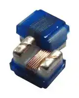
## **RF Inductor**

## **Automotive Grade AWCM Series**

## **Overview**

Wire-wound RF inductors are electronic components designed to store energy in a magnetic field when electrical current passes through them. They are constructed by winding a conductive wire (usually copper or gold-plated) around a core material such as air, ceramic, or ferrite.

This configuration allows them to provide high inductance values with minimal power loss, especially at high frequencies.

## **Benefits**

1. High Q-Factor (Quality Factor)

2. Wide Frequency Range

3. Low Signal Loss

4. High Current Handling

5. Can maintain excellent thermal stability at different temperatures

## **Applications**

1. Automotive Electronics: infotainment systems, ADAS, and car keyless entry systems.

2. Industrial and Medical Equipmen: RFID systems and medical imaging equipment.

3. Data Centers and Networking

4. Consumer Electronics

## **Product Information**

|**Series**|**Size Code (JIS/EIA)**|**Inductance (nH)**|
|---|---|---|
|AWCM|1005/0402|1.5 ~ 470|
||1608/0603||


AEC-Q200

## **AWCM00161008  Series Specification**

**1 Scope:** This specification applies to Wire Wound Ceramic Chip Inductors ~~_|~~

**==> picture [122 x 21] intentionally omitted <==**

**----- Start of picture text -----**<br>
2 [Part Numbering: ]<br>_|<br>**----- End of picture text -----**<br>


## **3 Rating:** ~~_|~~

Operating Temperature: - 40℃ ~ 125℃ (Including self - temperature rise) Storage Temperature: - 40℃ ~ 125℃ (The storage temperature range is for after the as **4 Marking:** ~~_|~~

**==> picture [182 x 21] intentionally omitted <==**

**----- Start of picture text -----**<br>
5 [Standard Testing Condition]<br>_|<br>**----- End of picture text -----**<br>


|**[Standard Testing Condition]**<br>~~_|~~|**[Standard Testing Condition]**||
|---|---|---|
||Unless otherwise specified|Incase ofdoubt|
|Temperature|OrdinaryTemperature(15to 35℃)|20 to 30℃|
|Humidity|OrdinaryHumidity(25to 85%RH)|50to 80 %RH|


AEC-Q200

## **AWCM00161008  Series Specification**

## **6 Configuration and Dimensions and Unit Weight:**

## **7 Electrical Characteristics:**

|**Part No.**|**Inductance**|**L/Q Test Freq.**|**Q**|**SRF**|**RDC**|**Irms**|**Tolerance**|
|---|---|---|---|---|---|---|---|
||**(nH)**|**(MHz)**|**Min.**|**(MHz)Min.**|**(Ω)Max.**|**(mA)Max.**||
|AWCM001610082N2□00|2.2|100/250|16|6000|0.049|700|B,C,D|
|AWCM001610083N6□00|3.6|100/250|25|6000|0.059|850|H,J|
|AWCM001610083N9□00|3.9|100/250|35|6000|0.059|850|H,J|
|AWCM001610084N3□00|4.3|100/250|35|6000|0.059|850|H,J|
|AWCM001610084N7□00|4.7|100/250|35|6000|0.059|850|H,J|
|AWCM001610085N6□00|5.6|100/250|35|6000|0.082|750|H,J|
|AWCM001610086N2□00|6.2|100/250|35|6000|0.082|750|H,J|
|AWCM001610086N8□00|6.8|100/250|35|6000|0.082|750|H,J,D|
|AWCM001610087N5□00|7.5|100/250|35|6000|0.082|750|H,J|
|AWCM001610088N2□00|8.2|100/250|35|6000|0.11|650|H,J,G|
|AWCM001610088N7□00|8.7|100/250|35|6000|0.11|650|H,J|
|AWCM001610089N1□00|9.1|100/250|35|6000|0.11|650|H,J|
|AWCM001610089N5□00|9.5|100/250|35|6000|0.11|650|H,J,G|
|AWCM0016100810N□00|10|100/250|35|6000|0.11|650|G,J|
|AWCM0016100811N□00|11|100/250|35|6000|0.11|650|G,J|
|AWCM0016100812N□00|12|100/250|35|6000|0.13|600|G,J|
|AWCM0016100813N□00|13|100/250|35|6000|0.13|600|G,J|
|AWCM0016100815N□00|15|100/250|40|6000|0.13|600|G,J|
|AWCM0016100816N□00|16|100/250|40|5500|0.16|550|G,J|
|AWCM0016100818N□00|18|100/250|40|5500|0.16|550|G,J|
|AWCM0016100820N□00|20|100/250|40|4900|0.16|550|G,J|
|AWCM0016100822N□00|22|100/250|40|4600|0.17|500|G,J|
|AWCM0016100824N□00|24|100/250|40|3800|0.21|500|G,J|
|AWCM0016100827N□00|27|100/250|40|3700|0.21|440|G,J|
|AWCM0016100830N□00|30|100/250|40|3300|0.23|420|G,J|


**NOTE: □-tolerance B=±0.1nH / C=±0.2nH / D=±0.5nH / H=±3%/ J=±5% / G=±2%**

1.Operating temperature range - 40℃ ~ 125℃

2.Irms for a 15℃ temperature rise from 25℃ ambient.

3.L/Q Test OSC @200mV.

4.Inductance would be correct Chilisin standard piece. 5.Offset value : -0.771nH

## ~~a~~ **AWCM00161008  Series Specification** AEC-Q200

**==> picture [457 x 400] intentionally omitted <==**

**----- Start of picture text -----**<br>
|||||||||
|---|---|---|---|---|---|---|---|
|Part No.|Inductance|L/Q Test Freq.|Q|SRF|RDC|Irms|Tolerance|
|(nH)|(MHz)|Min.|(MHz)Min.|(Ω)Max.|(mA)Max.|
|AWCM0016100833N□00|33|100/250|40|3200|0.23|420|G,J|
|AWCM0016100836N□00|36|100/250|40|2900|0.26|400|G,J|
|AWCM0016100839N□00|39|100/250|40|2800|0.26|400|G,J|
|AWCM0016100843N□00|43|100/200|40|2700|0.29|380|G,J|
|AWCM0016100847N□00|47|100/200|38|2600|0.29|380|G,J|
|AWCM0016100851N□00|51|100/200|38|2500|0.33|370|G,J|
|AWCM0016100856N□00|56|100/200|38|2400|0.35|360|G,J|
|AWCM0016100862N□00|62|100/200|38|2300|0.51|280|G,J|
|AWCM0016100868N□00|68|100/200|38|2200|0.38|340|G,J|
|AWCM0016100872N□00|72|100/150|34|2100|0.56|270|G,J|
|AWCM0016100875N□00|75|100/150|34|2050|0.56|270|G,J|
|AWCM0016100882N□00|82|100/150|34|2000|0.6|250|G,J|
|AWCM0016100891N□00|91|100/150|34|1900|0.64|230|G,J|
|AWCM00161008R10□00|100|100/150|34|1800|0.68|220|G,J|
|AWCM00161008R11□00|110|100/150|32|1700|1.2|200|G,J|
|AWCM00161008R12□00|120|100/150|32|1600|1.3|180|G,J|
|AWCM00161008R13□00|130|100/150|32|1450|1.4|170|G,J|
|AWCM00161008R15□00|150|100/150|32|1400|1.5|160|G,J|
|AWCM00161008R16□00|160|100/150|32|1350|2.1|150|G,J|
|AWCM00161008R18□00|180|100/100|25|1300|2.2|140|G,J|
|AWCM00161008R20□00|200|100/100|25|1250|2.4|120|G,J|
|AWCM00161008R22□00|220|100/100|25|1200|2.5|120|G,J|
|AWCM00161008R27□00|270|100/100|30|960|3.4|110|G,J|
|AWCM00161008R33□00|330|100/100|30|800|5.5|85|G,J|
|AWCM00161008R39□00|390|100/100|30|800|6.2|80|G,J|
|AWCM00161008R47□00|470|100/100|30|700|7|75|G,J|

**----- End of picture text -----**<br>


**NOTE: □-tolerance B=±0.1nH / C=±0.2nH / D=±0.5nH / H=±3%/ J=±5% / G=±2%** 1.Operating temperature range - 40℃ ~ 125℃ 2.Irms for a 15℃ temperature rise from 25℃ ambient. 3.L/Q Test OSC @200mV. 4.Inductance would be correct Chilisin standard piece. 5.Offset value : -0.771nH

**AWCM00161008  Series Specification** AEC-Q200

**==> picture [156 x 30] intentionally omitted <==**

**----- Start of picture text -----**<br>
8 AWCM00161008 Series<br>_<br>8.1 Construction:<br>**----- End of picture text -----**<br>


## **8.2 Material List:**

|NO|PART|MATERIAL|
|---|---|---|
|1|WIRE|Grade  180|
|2|EPOXY|UV GLUE|
|3|CORE|CERAMIC|
|4|TERMINAL|Ag/Ni/Sn|


AEC-Q200

## **AWCM00161008  Series Specification**

||**9**|**Reliability Of Ceramic Wire Wound Chip Inductor/CERAMIC SERIES**|**Reliability Of Ceramic Wire Wound Chip Inductor/CERAMIC SERIES**|**Reliability Of Ceramic Wire Wound Chip Inductor/CERAMIC SERIES**|||
|---|---|---|---|---|---|---|
||**1-1.Mechanical Performance**||||||
|**Item**<br>**Specification**<br>1-1-1 Board Flex<br>The forces applied on the right Test device shall be soldered on the substrate<br>conditions must not damage<br>Substrate Dimension: 100x40x1.6mm<br>the terminal electrode and the<br>Deflection: 2.0mm<br>ferrite.<br>Keeping Time: 60 sec<br>1-1-2 Terminal Strength<br>The chip must not damage the Refer to AEC-Q200-006<br>terminal electrode and the<br>Test device shall be soldered on the substrate<br>**TestMethod**<br>~~SS~~<br>~~{off~~<br>~~wee~~|||||||
||||ferrite.|Force 0.5lbs for 60±1 seconds for 0201 series|||
|||||Force 1lbs for 60±1 seconds for 0402 series|||
|||||Force 2lbs for 60±1 seconds for 0603 series|||
|||||Force 1.8Kgfor 60±1 seconds for the other series.|for 60±1 seconds for the other series.||
||1-1-3|Solderability|The electrodes shall be at|Pre-heating: 150℃, 1min|||
||||least 95% covered with new|Solder Composition: Sn/3.0Ag/0.5Cu|||
||||solder coating.|Solder Temperature: 245±5℃|||
|||||Immersion Time: 4±1sec|||
||1-1-4|Resistance to|Appearance:No damage|Pre-heating: 150℃, 1min|||
|||Soldering Heat|Inductance change shall|Solder Composition: Sn/Ag3.0/Cu0.5|||
||||be within ±10%.|Solder Temperature: 260±5℃|||
||||Q change:within±30% of||||
|initial value<br>1-1-5 ~~Resistance to~~<br>Solvents<br>There must be no change in<br>appearance or obliteration of<br>marking.<br>1-1-6 Mechanical Shock<br>The forces applied on the right Pulse shape<br>conditions must not damage<br>the terminal electrode and the<br>ferrite.<br>~~a~~||||Immersion Time: 10±1sec<br>Inductors must withstand 6 minutes of alcohol or water.<br>The forces applied on the right Pulse shape:Half-sine waveform<br>Impact acceleration:100 g<br>Pulse duration:6 ms<br>Number of shocks:18 shocks (3 shocks for each face)<br>Orientation:Bottom,top,left,right,front and rear faces|||
||1-1-7|Vibration|Appearance:No damage|Vibration waveform: Sine waveform|||
||||Inductance change shall be|Vibration frequency: 10Hz~2000Hz|||
||||within ±10%.|Vibration acceleration: 5g|||
||||Q change:within±30% of|Sweep rate: 0.764386otcave/minute|||
||||initial value|Duration of test: 12 cycles each of 3 orientations|||
|||||20 minutes for each cycle|||
|||||Vibration axes: X,Y & Z|||
||**1-2.Environmental Performance**||||||
|**No**<br>**Item**<br>**Specification**<br>1-2-1 High Temperature<br>Appearance:No damage (for<br>Exposure (Storage)<br>microscope of CASTOR MZ-45 <br>20X)Inductance change shall<br>1-2-2 Low Temperature<br>be within ±10%.<br>Exposure (Storage)<br>Q change:within±30% of<br>initial value<br>1-2-3 Biased Humidity<br>1-2-4 Temperature Cycling<br>~~ee~~<br>~~{oo~~<br>~~= ~~||||Temperature: 125±3℃<br> Time: 1000hrs<br>Measured after exposure in the room condition for 24hrs<br>Temperature: -40±3℃<br>Time: 1000hrs<br>Measured after exposure in the room condition for 24hrs<br>Temperature: 85±2℃<br>Relative Humidity: 85%<br>Time: 1000hrs<br>Measured after exposure in the room condition for 24hrs<br>Total cycles: 1000 cycles<br>**Test Method**<br>~~SC~~<br> ~~ee~~|||
|||||Temperature Cycling Test Conditions : -40 to +125℃|||
|||||Soak Mode Condition :  30 minutes|||
|||||Measured after exposure in the room condition for 24hrs|||
||1-2-5|Operational Life|Appearance:No damage|Temperature: 125±2℃|||
||||Inductance change shall|Appliend Current : Rated Current|||
||||be within ±10%.|Time: 1000± 24 hrs|||
|||||Measured after exposure in the room condition for 24hrs|||
||1-2-6|ESD||Test mode:Contact Discharge|||
|||||Discharge level:±6KV, Discharge interval:1 second|||
|||||Polarity of the output voltage:Positive and negative|Positive and negative||
|||||Number of discharge:Discharge +/- for 1 time for the 2 test|||
|||||points.|||
|||||Test Mode:Air Discharge|||
|||||Discharge level:±12KV, ±16KV, ±25KV|||
|||||Discharge interval:<5 seconds|||
|||||Polarity of the output voltage:Positive and negative|Positive and negative||
|||||Number of discharge:Discharge +/- for 1 time for the 1~2 test|||
|||||points.|||


**AWCM00161008  Series Specification** AEC-Q200

**==> picture [493 x 20] intentionally omitted <==**

**----- Start of picture text -----**<br>
AWCM00161008  Series Specification AEC-Q200<br>**----- End of picture text -----**<br>


**==> picture [482 x 537] intentionally omitted <==**

**----- Start of picture text -----**<br>
10 Packaging:<br>_ |<br>10.1 Packaging -Cover Tape<br>The force for tearing off cover tape is 10 to 100 grams in the arrow direction.<br>\ / 185°to180<br>CARRIER \\BASE TAPE<br>10.2 Packaging Quantity<br>TYPE PCS/REEL<br>161008 4000<br>10.3 Reel Dimensions<br>Dimensions in mm<br>TYPE A B C D<br>161008 178±1 60±0.5 12±0.5 1.5±0.5<br>**----- End of picture text -----**<br>


**AWCM00161008  Series Specification** AEC-Q200

**==> picture [386 x 214] intentionally omitted <==**

**----- Start of picture text -----**<br>
10 Packaging:<br>10.4 Tape Dimensions in mm<br>sna Tape Material<br>1 440.1 CoverCarrier tane:tape :PolyethyleneP<br>- —--j--- =e<br>! TT Beams, 5) A<br>|<br>Epi |<br>Cc 460mm hlN [Chip Mountinghéomm hl<br>Trail Part Part Blank<br>Cover<br>Tape<br>TYPE A B C D E F G T<br>161008 8.0 1.20 4 1.80 3.5 1.75 2 1.05<br>**----- End of picture text -----**<br>


## **11 Recommended Land Pattern:**

**==> picture [263 x 41] intentionally omitted <==**

**----- Start of picture text -----**<br>
Dimensions in mm<br>TYPE H(In/mm) I(In/mm) J(In/mm)<br>161008 0.04/1.02 0.025/0.64 0.025/0.64<br>**----- End of picture text -----**<br>


## **12 Note:**

1. Please make sure that your product has been evaluated and confirmed against your specifications when our product is mounted to your product.

2. Do not knock nor drop.

3. All the items and parameters in this product specification have been prescribed on the premise that our product is used for the purpose,under the condition and in the environment agreed upon between you and us. You are requested not to use our product deviating from  such agreement. 4.The storage period is less than 12 months. Be sure to follow the storage conditions (Temperature: 5 to 40°C, Humidity: 10 to 75% RHor less). If the storage period elapses, the soldering of the terminal   electrodes may deteriorate. 5.Do not use or store in locations where there are conditions such as gas corrosion (salt, acid, alkali, etc.).

6. The moisture sensitivity level (MSL) of products is classified as level 1.

AEC-Q200

## **AWCM00161008  Series Specification**

**==> picture [59 x 12] intentionally omitted <==**

**----- Start of picture text -----**<br>
13 Graph:<br>**----- End of picture text -----**<br>


## **AWCM00161008  Series Specification** AEC-Q200

AEC-Q200

## **AWCM00161008  Series Specification**

AEC-Q200

##

AEC-Q200

##

**AWCM00161008  Series Specification** AEC-Q200

**AWCM00161008  Series Specification** AEC-Q200
Updated at June 4, 2026
Pulse Electronics, a YAGEO company, is a global leader in the design and manufacturing of passive electronic components. With a legacy of innovation dating back to 1956, the company provides essential technology for the communications, computing, industrial, transportation, and IoT sectors. Pulse is recognized worldwide for delivering high-performance solutions that power advanced applications, ranging from 5G networks and electric vehicles to data centers and smart grids. The company's extensive product portfolio is heavily anchored in power and networking magnetics. This includes a comprehensive range of power inductors engineered for exceptional efficiency and reliability in demanding environments. To address complex electromagnetic compatibility challenges, Pulse also manufactures highly effective EMC and RFI suppression solutions, such as common mode chokes and filters, alongside specialized toroidal and RF inductors designed to ensure clean power delivery and optimal signal integrity. Beyond traditional magnetics, Pulse excels in the development of advanced wireless and power conversion components. Their connectivity solutions feature a wide array of high-performance RF antennas and single-band chip antennas tailored for modern connected devices. Furthermore, to support sophisticated power architectures, Pulse provides a broad spectrum of transformers—encompassing PCB-mounted designs, current sensing transformers, and precise pulse transformers—equipping engineers with robust, industry-proven components for power isolation and measurement.
About Novapart
Novapart is a B2B electronic component broker specialising in stock shortages and cost reduction. We source hard-to-find parts and identify compliant alternatives across a catalogue of 410,000+ components from 500+ manufacturers.
Learn more →Stock Shortage Specialist
When a component is unavailable, discontinued or has an unacceptable lead time, we tap into our network of vetted European and Asian distributors to source what you need — without compromising on quality or traceability.
Request a quote →Compliant Alternatives
We identify pin-to-pin, electrically equivalent substitutes that meet the same certifications (RoHS, AEC-Q100, REACH) as your original specification — validated against datasheets, not just part numbers. Often at a lower cost.
BOM Analysis service →