


AUIRGPS4070D0
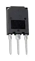
IGBT, 240 A, 1.7 V, 750 W, 600 V, TO-274, 3 Pins
- Manufacturer: INFINEON
- Product type: Single IGBTs
- DC Collector Current:240A; Collector Emitter Saturation Voltage Vce(on):1.7V; Power Dissipation Pd:750W; Collector Emitter Voltage V(br)ceo:600V; Transistor Case Style:TO-274; No
- MSL: MSL 1 - Unlimited
- SVHC: No SVHC (25-Jun-2025)
- No. of Pins: 3Pins
- Product Range: -
- Power Dissipation: 750W
- Transistor Mounting: Through Hole
- Transistor Case Style: TO-274
- Operating Temperature Max: 175°C
- Continuous Collector Current: 240A
- Collector Emitter Voltage Max: 600V
- Collector Emitter Saturation Voltage: 1.7V
| Delivery and price | |
|---|---|
| Units per pack | 250 |
| Price | 9.39 € |
| Current stock | 10+ |
| Lead time | 30 days |
~~Cinfineon~~ **AUTOMOTIVE GRADE** AUIRGPS4070D0 ~~a~~ _**INSULATED GATE BIPOLAR TRANSISTOR WITH ULTRAFAST SOFT RECOVERY DIODE**_ **Features** Low VCE (on) Trench IGBT Technology C VCES = 600V Low Switching Losses IC = 160A, TC = 100°C 6µs SCSOA Square RBSOA G tsc 6µs, TJ(MAX) = 175°C 100% of the parts tested for ILM[] E VCE(on) typ. = 1.70V n-channel Positive VCE (on) Temperature Coefficient Soft Recovery Co-pak Diode o] Lead-Free, RoHS Compliant C Automotive Qualified * **Benefits** High Efficiency in a Wide Range of Applications Suitable for Applications in the Low to Mid-Range Frequencies G C[E ] Rugged Transient Performance for Increased Reliability PG-TO274-3-903 Excellent Current Sharing in Parallel Operation Low EMI G C E Gate Collector Emitter ~~———~~ **Standard Pack Base Part Number Package Type Orderable Part Number Form Quantity** AUIRGPS4070D0 PG-TO274-3-903 Tube 25 AUIRGPS4070D0 ~~Se~~ **Absolute Maximum Ratings** ~~ee ee~~ Stresses beyond those listed under “Absolute Maximum Ratings” may cause permanent damage to the device. These are stress ratings only; and functional operation of the device at these or any other condition beyond those indicated in the specifications is not implied. Exposure to absolute-maximum-rated conditions for extended periods may affect device reliability. The thermal resistance and power dissipation ratings are measured under board mounted and still air conditions. Ambient temperature (TA) is 25°C, unless otherwise specified. ||**Parameter**|**Max.**|**Units**| |---|---|---|---| |VCES|Collector-to-Emitter Voltage|600|V| |IC @TC= 25°C|Continuous Collector Current|240|A| |IC @TC= 100°C|Continuous Collector Current|160|| |INOMINAL|Nominal Current|120|| |ICM|Pulse Collector Current,VGE= 15V|360|| |ILM|ClampedInductiveLoad Current,VGE= 20V|480|| |IF NOMINAL|Diode Nominal Current|120|| |IFM|Diode Maximum Forward Current|480|| |VGE|Continuous Gate-to-Emitter Voltage|±20|V| ||Transient Gate-to-Emitter Voltage|±30|| |PD @TC= 25°C|Maximum Power Dissipation|750|W<br>| |PD @TC= 100°C<br>~~pf~~|Maximum Power Dissipation<br>~~pf~~|375<br>|| |TJ<br>TSTG<br>~~pf~~|Operating Junction and<br>Storage Temperature Range<br>~~pffd~~|-55 to +175<br>~~fd~~|°C<br>~~fd~~| |~~pf~~|Soldering Temperature, for 10 sec.<br>~~pffd~~|300 (0.063 in. (1.6mm) from case)<br>~~fd~~|| ## **Thermal Resistance** ||**Parameter**|**Typ.**|**Max. Units**|**Max. Units**| |---|---|---|---|---| |RJC (IGBT)|Thermal Resistance Junction-to-Case(each IGBT) |–––|0.20|°C/W| |RJC(Diode)|Thermal Resistance Junction-to-Case(each Diode) |–––|0.45|| |RCS|Thermal Resistance,Case-to-Sink(flat, greased surface)|0.24|–––|| |RJA|Thermal Resistance,Junction-to-Ambient(typical socket mount)|–––|40|| * Qualification standards can be found at www.infineon.com V 2.4 1 2018-12-03 ## ~~Cinfin eon~~ ## AUIRGPS4070D0 ~~_~~ |<br>AUIRGPS4070D0<br>~~Cinfineon~~<br>~~_~~|| |---|---| |**Electrical Characteristics@ TJ = 25°C(unless otherwise specified)**|| |**Parameter**<br>**Min.**<br>**Typ. **<br>**Max. Units**<br>**Conditions**<br>V(BR)CES<br>Collector-to-Emitter Breakdown Voltage<br>600<br>—<br>—<br>V<br>VGE =0V, IC =500µA<br>V(BR)CES/TJTemperature Coeff. of Breakdown Voltage<br>—<br>0.74<br>—<br>V/°C VGE= 0V,IC= 5mA(25°C-175°C)<br>VCE(on)<br>Collector-to-Emitter Saturation Voltage<br>—<br>1.7<br>2.0<br>V<br>IC= 120A,VGE= 15V,TJ= 25°C<br>—<br>2.0<br>—<br>IC =120A, VGE =15V, TJ =150°C<br>—<br>2.1<br>—<br>IC =120A, VGE =15V, TJ =175°C<br>~~es~~<br>~~nn~~<br>~~GR~~<br>~~es~~<br>~~nD(OD IYQO~~<br>~~es~~<br>~~I GDQU (~~<br>~~ee~~|| |VGE(th)<br>GateThresholdVoltage<br>4.0<br>—<br>6.5<br>V<br>VCE= VGE,IC=5.6mA<br>VGE(th)/TJThreshold Voltage temp. coefficient<br>—<br>-16<br>—<br>mV/°C VCE= VGE,IC= 5.6mA(25°C-175°C)<br>gfe<br>Forward Transconductance<br>—<br>87<br>—<br>S<br>VCE =50V, IC =120A<br>Collector-to-Emitter Leakage Current<br>—<br>1.0<br>200<br>µAVGE =0V, VCE =600V<br>—<br>2.0<br>—<br>mA<br>VGE= 0V,VCE= 600V,TJ= 175°C<br>ICES<br>~~a~~<br>~~ee ee~~<br>~~EEE~~|| |VFM<br>Diode Forward Voltage Drop<br>—<br>1.8<br>2.1<br>VIF= 120A<br>—<br>1.9<br>—<br>IF= 120A,TJ= 175°C<br>IGES<br>Gate-to-Emitter Leakage Current<br>—<br>—<br>±100<br>nA<br>VGE= ±20V<br>~~rr~~<br>~~ee~~<br>~~I (RD (ROD (OR~~|| |**Switching Characteristics@ TJ = 25°C(unless otherwise specified)**|| |**Parameter**<br>**Min.**<br>**Typ.**<br>**Max. Units**<br>**Conditions**<br>Qg<br>Total Gate Charge (turn-on)<br>—<br>250<br>375<br>nC<br>IC= 120A<br>Qge<br>Gate-to-Emitter Charge (turn-on)<br>—<br>65<br>98<br>VGE= 15V<br>Qgc<br>Gate-to-Collector Charge (turn-on)<br>—<br>100<br>150<br>VCC= 400V<br>Eon<br>Turn-On Switching Loss<br>—<br>5.7<br>6.7<br>mJ<br>Eoff<br>Turn-Off Switching Loss<br>—<br>4.2<br>5.2<br>Etotal<br>TotalSwitchingLoss<br>—<br>9.9<br>11.9<br>IC= 120A, VCC= 400V, VGE= 15V<br>~~————~~<br>~~ee ee ae a~~<br>~~ne~~<br>~~ee~~<br>~~—ae~~|| |td(on)<br>Turn-On delaytime<br>—<br>40<br>60<br>ns<br>RG= 4.7, L = 87µH, TJ= 25°C<br>tr<br>Rise time<br>—<br>125<br>155<br>Energy losses include tail & diode<br>td(off)<br>Turn-Off delaytime<br>—<br>140<br>170<br>reverse recovery<br>tf<br>Fall time<br>—<br>120<br>170<br>Eon<br>Turn-On Switching Loss<br>—<br>6.4<br>—<br>mJ<br>Eoff<br>Turn-Off Switching Loss<br>—<br>4.7<br>—<br>Etotal<br>Total Switching Loss<br>—<br>11.1<br>—<br>IC= 120A, VCC= 400V, VGE= 15V<br>td(on)<br>Turn-On delaytime<br>—<br>40<br>—<br>ns<br>RG= 4.7, L = 87µH, TJ= 175°C<br>tr<br>Rise time<br>—<br>110<br>—<br>Energy losses include tail & diode<br>td(off)<br>Turn-Off delay time<br>—<br>160<br>—<br>reverse recovery<br>tf<br>Fall time<br>—<br>125<br>—<br>Cies<br>Input Capacitance<br>—<br>7600<br>—<br>pF<br>VGE= 0V<br>Coes<br>Output Capacitance<br>—<br>510<br>—<br>VCC= 30V<br>Cres<br>Reverse Transfer Capacitance<br>—<br>230<br>—<br>f = 1.0Mhz<br>TJ= 175°C, IC= 480A<br>RBSOA<br>Reverse Bias Safe Operating Area<br>FULL SQUARE<br>VCC= 480V, Vp ≤ 600V<br>Rg=4.7, VGE = +20V to 0V<br>SCSOA<br>Short Circuit Safe Operating Area<br>6<br>—<br>—<br>VCC= 400V, Vp ≤ 600V<br>Rg=5.0, VGE = +15V to 0V<br>Erec<br>ReverseRecoveryEnergy oftheDiode<br>—<br>1740<br>—<br>µJ<br>TJ= 175°C<br>trr<br>Diode Reverse Recovery Time<br>—<br>210<br>—<br>ns<br>VCC= 400V, IF= 120A<br>Irr<br>Peak Reverse RecoveryCurrent<br>—<br>45<br>—<br>A<br>VGE= 15V,Rg= 4.7,L = 87µH<br>µs<br>~~——~~<br>~~ee—————~~<br>~~esa~~<br>~~——————a~~<br>~~esen~~<br>~~po~~<br>~~pf ff~~<br>~~———————————~~|| |**Notes:**|| | VCC= 80% (VCES), VGE= 20V, L = 3.5µH, RG= 47tested in production ILM400A.|| - Pulse width limited by max. junction temperature. - Refer to AN-1086 for guidelines for measuring V(BR)CES safely. - R is measured at TJ approximately 90°C. - Calculated continuous current based on maximum allowable junction temperature. Package IGBT current limit is 195A. Package diode current limit is120A. Note that current limitations arising from heating of the device leads may occur. 2 V 2.4 ~~re~~ 2018-12-03 ~~Cafineon~~ AUIRGPS4070D0 ~~LLL~~ **==> picture [205 x 693] intentionally omitted <==** **----- Start of picture text -----**<br> 250<br>200<br>aw<br>150<br>CPN ET<br>100 PIN<br>50<br>EEEERS<br>0 Pe} ELEN<br>25 50 75 100 125 150 175<br> TC (°C)<br>Fig. 1 - Maximum DC Collector Current vs.<br>Case Temperature<br>1000<br>10µsec<br>100<br>100µsec<br>1msec<br>10<br>DC<br>1 me<br>Tc = 25°C<br>Tj = 175°C<br>Single Pulse<br>0.1<br>1 10 100 1000<br>VCE (V)<br>Fig. 3 - Forward SOA<br>TC = 25°C, TJ 175°C; VGE =15V<br>480<br>420 Tyr V V GEGE = 18V = 15V<br>VGE = 12V<br>360 V GE = 10V<br>300 otEO VGE = 8.0V<br>Fee =<br>240<br>180 A<br>120 7 a<br>60 fT<br>JSS<br>0<br>0 2 4 6 8 10<br> VCE (V)<br>Fig. 5 - Typ. IGBT Output Characteristics<br>TJ = -40°C; tp = 20µs<br>IC (A)<br>IC (A)<br>ICE (A)<br>**----- End of picture text -----**<br> **==> picture [203 x 194] intentionally omitted <==** **----- Start of picture text -----**<br> 800<br>700<br>600 PASCEECE<br>500<br>400 PCPS<br>300 FECES<br>200<br>100 FECES<br>0 CCEEECENS<br>0 20 40 60 80 100 120 140 160 180<br> TC (°C)<br>Ptot (W)<br>**----- End of picture text -----**<br> **Fig. 2** - Power Dissipation vs. Case Temperature **==> picture [206 x 432] intentionally omitted <==** **----- Start of picture text -----**<br> 1000<br>100<br>10<br>Samal<br>1<br>10 100 1000<br>VCE (V)<br>Fig. 4 - Reverse Bias SOA<br> TJ = 175°C; VGE = 20V<br>480<br>420 or V V GEGE = 18V = 15V<br>VGE = 12V<br>360 V GE = 10V<br>300 t=ah VGE = 8.0V<br>240 a<br>180 s/o<br>120 OTT<br>60 FEEEEET=<br>0 SORE<br>0 2 4 6 8 10<br> VCE (V)<br>IC (A)<br>ICE (A)<br>**----- End of picture text -----**<br> **Fig. 6** - Typ. IGBT Output Characteristics TJ = 25°C; tp = 20µs 3 ~~=~~ V 2.4 2018-12-03 AUIRGPS4070D0 ~~oe~~ ## ~~Giro~~ **==> picture [199 x 193] intentionally omitted <==** **----- Start of picture text -----**<br> 480<br>VGE = 18V<br>420 V GE = 15V<br>VGE = 12V<br>360 V GE = 10V<br>300 AS VGE = 8.0V<br>any 74<br>240<br>Pear<br>7<br>180<br>120<br>60 p=|<br>0 ALT<br>0 2 4 6 8 10<br> VCE (V)<br>ICE (A)<br>**----- End of picture text -----**<br> **Fig. 7** - Typ. IGBT Output Characteristics TJ = 175°C; tp = 20µs **==> picture [195 x 465] intentionally omitted <==** **----- Start of picture text -----**<br> 10<br>8 lta<br>ICE = 60A<br>6 I CE = 120A<br>ICE = 195A<br>4 |l ll<br>2<br>2a<br>0 | TP<br>5 10 15 20<br> VGE (V)<br>Fig. 9 - Typical VCE vs. VGE<br>TJ = -40°C<br>10<br>ICE = 60A<br>8 I CE = 120A<br>ICE = 195A<br>6 a<br>4 ry<br>2 =<br>f_<br>0 [|<br>5 10 15 20<br> VGE (V)<br>Fig. 11 - Typical VCE vs. VGE<br>TJ = 175°C<br>VCE (V)<br>VCE (V)<br>**----- End of picture text -----**<br> **==> picture [242 x 668] intentionally omitted <==** **----- Start of picture text -----**<br> 480<br>420<br>-40°C<br>360<br>25°C<br>PE 175°C<br>300 - Hf<br>240 a<br>// ae<br>180<br>120<br>a)ffZee<br>60<br>So<br>0<br>0.0 1.0 2.0 3.0 4.0 5.0<br> VF (V)<br>Fig. 8 - Typ. Diode Forward Characteristics<br>tp = 20µs<br>10<br>8 Lt<br>ICE = 60A<br>6 ICE = 120A<br>ICE = 195A<br>4 iaii<br>2<br>|<br>0 |TtWe<br>5 10 15 20<br> VGE (V)<br>Fig. 10 - Typical VCE vs. VGE<br>TJ = 25°C<br>480<br>420<br>TJ = -40°C<br>360 T J = 25°C<br>300 T J = 175°C a) ae<br>240<br>pf<br>180<br>120<br>I<br>60<br>s—<br>0 fe<br>4 6 8 10 12 14<br> VGE (V)<br>VCE (V)<br>ICE (A)<br>IF (A)<br>**----- End of picture text -----**<br> **Fig. 12** - Typ. Transfer Characteristics VCE = 50V; tp = 20µs 4 V 2.4 2018-12-03 AUIRGPS4070D0 **==> picture [490 x 681] intentionally omitted <==** **----- Start of picture text -----**<br> 25<br>1000<br>20<br>tdOFFOFF<br>15<br>EON tFF<br>100<br>10<br>tRR<br>EOFF<br>5 tdONON<br>0<br>0 50 100 150 200 250 10<br>0 50 100 150 200<br>IC (A)<br>IC (A)<br>Fig. 13 - Typ. Energy Loss vs. IC Fig. 14 - Typ. Switching Loss vs. IC<br>TJ = 175°C; L = 0.087mH; VCE = 400V, RG = 4.7; VGE = 15V TJ = 175°C; L = 0.087mH; VJ = 175°C; L = 0.087mH; V = 175°C; L = 0.087mH; VCE = 400V, RG = 4.7= 400V, RG = 4.7G = 4.7 = 4.7; VGE = 15V [ARE] CE = 400V, RG = 4.7= 400V, RG = 4.7G = 4.7 = 4.7; VGE = 15V<br>16 10000<br>14<br>12 E ON<br>10 1000 tdOFF<br>8<br>-| EOFF Ee tF<br>6<br>100 tR<br>Z| lee<br>4<br>tdON<br>2<br>0 10 Eannae<br>0 10 20 30 40 50 60 0 10 20 30 40 50 60<br>Rg () RG ()<br>Fig. 15 - Typ. Energy Loss vs. RG G Fig. 16 - Typ. Switching Time vs. RG<br> = 175°C; L = 0.087mH; VCE = 400V, ICE = 120A; VGE = 15V CE = 400V, ICE = 120A; VGE = 15V = 400V, ICE = 120A; VGE = 15V CE = 120A; VGE = 15V = 120A; VGE = 15V GE = 15V = 15V TJ = 175°C; L = 0.087mH; VCE = 400V, ICEJ = 175°C; L = 0.087mH; VCE = 400V, ICE = 175°C; L = 0.087mH; VCE = 400V, ICECE = 400V, ICE = 400V, ICECE = 120A; VGE = 15V<br>45 45<br>RG = 4.7<br>40 40<br>Ve}<br>35 R G = 35<br>t<br>30 30 ENE<br>RG = 20<br>25 25<br>P|] NEE<br>RG = 50<br>20 Ex 20 SEEee<br>0 50 100 150 200 250 0 10 20 30 40 50 60<br>IF (A) RG (<br>Energy (mJ)<br>Energy (mJ)<br>Swiching Time (ns)<br>Swiching Time (ns)<br>IRR (A) IRR (A)<br>**----- End of picture text -----**<br> **==> picture [199 x 193] intentionally omitted <==** **----- Start of picture text -----**<br> 1000<br>tdOFFOFF<br>tFF<br>100<br>tRR<br>tdONON<br>10<br>0 50 100 150 200 250<br>IC (A)<br>Swiching Time (ns)<br>**----- End of picture text -----**<br> **Fig. 14** - Typ. Switching Loss vs. IC TJ = 175°C; L = 0.087mH; VJ = 175°C; L = 0.087mH; V = 175°C; L = 0.087mH; VCE = 400V, RG = 4.7= 400V, RG = 4.7G = 4.7 = 4.7; VGE = 15V **Fig. 15** - Typ. Energy Loss vs. RG G TJ = 175°C; L = 0.087mH; VCE = 400V, ICE = 120A; VGE = 15V CE = 400V, ICE = 120A; VGE = 15V = 400V, ICE = 120A; VGE = 15V CE = 120A; VGE = 15V = 120A; VGE = 15V GE = 15V = 15V **Fig. 16** - Typ. Switching Time vs. RG TJ = 175°C; L = 0.087mH; VCE = 400V, ICEJ = 175°C; L = 0.087mH; VCE = 400V, ICE = 175°C; L = 0.087mH; VCE = 400V, ICECE = 400V, ICE = 400V, ICECE = 120A; VGE = 15V **Fig. 17** - Typ. Diode IRR vs. IF TJ = 175°C **Fig. 18** - Typ. Diode IRR vs. RG TJ = 175°C 5 V 2.4 2018-12-03 **==> picture [216 x 232] intentionally omitted <==** **----- Start of picture text -----**<br> Gafineon<br>45<br>40<br>35<br>30<br>25<br>20<br>PEE<br>200 400 600 800<br>diF /dt (A/µs)<br>IRR (A)<br>**----- End of picture text -----**<br> **==> picture [251 x 230] intentionally omitted <==** **----- Start of picture text -----**<br> AUIRGPS4070D0<br>LLL<br>10000<br>9000<br>240A<br>8000 4.7<br>10<br>7000 pc<br>20<br>6000 50 120A<br>5000<br>60A<br>a<br>4000<br>3000<br>P| tt<br>300 400 \ 500 600 AA 700 800<br>diF /dt (A/µs)<br>QRR (nC)<br>**----- End of picture text -----**<br> **Fig. 19** - Typ. Diode IRR vs. diF/dt VCC = 400V; VGE = 15V; IF = 120A; TJ = 175°C **Fig. 20** - Typ. Diode QRR vs. diF/dt VCC = 400V; VGE = 15V; TJ = 175°C **==> picture [528 x 435] intentionally omitted <==** **----- Start of picture text -----**<br> 24 1200<br>3000<br>RG = 4.7 20 1000<br>2500<br>RG = 10 a Att Tt) Isc<br>RG = 20<br>2000 R G = 50 16 800<br>T<br>sc<br>pe 12 ENGEp 4s 600<br>1500<br>inaa PENSE<br>8 400<br>1000<br>ea [Aan<br>4 200<br>500<br>pt | 9 E4RREEE 10 11 12 13 14 15 16<br>50 100 150 200 250<br>VGE (V)<br>IF (A)<br>Fig. 21 - Typ. Diode ERR vs. IF Fig. 22 - VGE vs. Short Circuit Time<br>TJ = 175°C VCC = 400V; TC = 25°C<br>100000 16<br>VCES = 400V<br>Cies VCES = 300V<br>10000 12<br>Too «6g<br>1000 8<br>Ser} Coes<br>100 4<br>Saaee Cres Fanaal<br>10 Sinn 0 AREEEE<br>0 100 200 300 400 500 0 50 100 150 200 250 300<br>VCE (V) Q G, Total Gate Charge (nC)<br>Capacitance (pF)<br>VGE, Gate-to-Emitter Voltage (V)<br>Energy (µJ) Time (µs) Current (A)<br>**----- End of picture text -----**<br> **Fig. 23** - Typ. Capacitance vs. VCE VGE= 0V; f = 1MHz **Fig. 24** - Typical Gate Charge vs. VGE ICE = 120A 6 V 2.4 2018-12-03 AUIRGPS4070D0 **==> picture [444 x 469] intentionally omitted <==** **----- Start of picture text -----**<br> 1<br>0.1 D = 0.50<br>0.20<br>°<br>0.10 Ri ( C/W) I (sec)<br>0.01 0.05 R1R1 R2R2 R3R3 R 4R4 0.00442 0.000014<br>0.02 J J C C 0.04530 0.000165<br>0.01 1 1 2 2 3 3 4 4 0.08912 0.004938<br>0.001 SINGLE PULSE — CiCi= =iRiiRi / 0.06121 0.026150<br>( THERMAL RESPONSE ) Notes:<br>1. Duty Factor D = t1/t2<br>2. Peak Tj = P dm x Zthjc + Tc<br>0.0001<br>1E-006 1E-005 0.0001 0.001 0.01 0.1<br>t1 , Rectangular Pulse Duration (sec)<br>Fig 25. Maximum Transient Thermal Impedance, Junction-to-Case (IGBT)<br>1<br>TC<br>D = 0.50<br>0.1 0.20<br>Ph TMCTU<br>0.10<br>°<br>0.05 Ri ( C/W) I (sec)<br>0.01 0.02 R1 R1 R2 R2 R3 R3 R 4R 4 0.00948 0.000013<br>Tr 0.01 diese J J IN | |} C C 0.12750 0.000134<br>et rey 1 1 oo 2 2 3 3 4 4 0.18573 0.003167<br>0.001 eal Ci= Ci i =iRiiRi 0.12730 0.020010<br>Notes:<br>SINGLE PULSE<br>1. Duty Factor D = t1/t2<br>( THERMAL RESPONSE )<br>2. Peak Tj = P dm x Zthjc + Tc<br>0.0001 Sime |<br>1E-006 1E-005 0.0001 0.001 0.01 0.1<br>t1 , Rectangular Pulse Duration (sec)<br>Thermal Response ( Z thJC )<br>Thermal Response ( Z thJC )<br>**----- End of picture text -----**<br> **Fig 26.** Maximum Transient Thermal Impedance, Junction-to-Case (DIODE) 7 V 2.4 ~~——_—__--~~ V 2.4 2018-12-03 ~~Cinfineon~~ AUIRGPS4070D0 ~~_~~ **==> picture [472 x 105] intentionally omitted <==** **----- Start of picture text -----**<br> L<br>L<br>DUT VCC 80 V +<br>0<br>1K - DUT VCC<br>Rg<br>**----- End of picture text -----**<br> Gate Charge Circuit **==> picture [71 x 9] intentionally omitted <==** **----- Start of picture text -----**<br> RBSOA Circuit<br>**----- End of picture text -----**<br> **Fig.C.T.1** - Gate Charge Circuit (turn-off) **Fig.C.T.2** - RBSOA Circuit **==> picture [81 x 109] intentionally omitted <==** **----- Start of picture text -----**<br> 4X<br>DC VCC<br>DUT<br>RSH<br>**----- End of picture text -----**<br> **Fig.C.T.3** - S.C. SOA Circuit **==> picture [170 x 101] intentionally omitted <==** **----- Start of picture text -----**<br> R = [VCC]<br>ICM<br>VCC<br>DUT<br>Rg<br>**----- End of picture text -----**<br> **==> picture [197 x 413] intentionally omitted <==** **----- Start of picture text -----**<br> diode clamp /<br>DUT<br>L<br>><br>-5V<br>DUT / VCC<br>DRIVER<br>;<br>Rg<br>Switching Loss<br>Fig.C.T.4 - Switching Loss Circuit<br>C force<br>100K<br>D1 22K<br>C sense<br>DUT<br>G force 0.0075µF<br>E sense<br>E force<br>**----- End of picture text -----**<br> **Fig.C.T.5** - Resistive Load Circuit **Fig.C.T.6** - BVCES Filter Circuit 8 V 2.4 **==> picture [544 x 669] intentionally omitted <==** **----- Start of picture text -----**<br> AUIRGPS4070D0<br>EEE—<§ |<br>600 180<br>600 180<br>tf<br>tr<br>500 150<br>500 150<br>TEST CURRENT<br>400 120<br>400 120<br>300 a ieee 90 le 90% ICE<br>90% ICE 300 90<br>200 60<br>200 60<br>10% ICE 10%ICE<br>100 30<br>a 100 ne 30<br>10% VCE 10% VCE<br>0 0<br>0 0<br>| an NiE-<br>Eoff Loss<br>Eon Loss<br>-100 -30<br>-100 -30<br>0 0.5 1 1.5<br>0 0.5 1 1.5<br>time(µs)<br>time (µs)<br>Fig. WF1 - Typ. Turn-off Loss Waveform Fig. WF2 - Typ. Turn-on Loss Waveform<br>@ TJ = 175°C using Fig. CT.4 @ TJ = 175°C using Fig. CT.4<br>140<br>500<br>— QRR<br>120<br>VCECE<br>a<br>100 400<br>80<br>tRR<br>300<br>fe<br>60 ICECE<br>40<br>200<br>20 eeeee<br>0 ee 100<br>-20 Peak<br>IRR<br>nye 0 0<br>-40 \<br>c e<br>-60<br>-0.40 0.10 0.60 1.10 -100<br>-4.00 0.00 4.00 8.00 12.00<br>time (µS)<br> (V) (A)<br>VCE ICE (V)VCE (A)ICE<br> (A)<br>IF<br>Vce (V)<br>**----- End of picture text -----**<br> **==> picture [231 x 257] intentionally omitted <==** **----- Start of picture text -----**<br> 500 2000<br>VCECE<br>400 1600<br>300 1200<br>ICECE<br>200 800<br>100 400<br>0 0<br>-100 -400<br>-4.00 0.00 4.00 8.00 12.00<br>Time (uS)<br>Ice (A)<br>Vce (V)<br>**----- End of picture text -----**<br> **Fig. WF3** - Typ. Diode Recovery Waveform @ TJ = 175°C using Fig. CT.4 **Fig. WF4** - Typ. S.C. Waveform @ TJ = 25°C using Fig. CT.3 9 V 2.4 ~~EO~~ V 2.4 2018-12-03 AUIRGPS4070D0 ~~_~~ ## ~~Cinfineon~~ Case Outline and Dimensions-PG-TO274-3-903 (Dimensions are shown in millimeters (inches)) ## PG-TO274-3-903 -Part Marking Information **==> picture [371 x 147] intentionally omitted <==** **----- Start of picture text -----**<br> Part Number AUGPS4070D0<br>Date Code<br>YWWA Y = Year<br>IR Logo 1 éaR WW = Work Week<br>A = Automotive, Lead Free<br><br>XX XX<br>|<br>Lot Code<br>**----- End of picture text -----**<br> 10 V 2.4 2018-12-03 ~~Cinfineon~~ AUIRGPS4070D0 ~~_~~ **Qualification Information** Automotive (per AEC-Q101) **Qualification Level** This part number(s) passed Automotive qualification. Infineon’s Industrial and Consumer qualification level is granted by extension of the higher Automotive level. **Moisture Sensitivity Level** PG-TO274-3-903 N/A Class H3B(+/‐ 8000)[† ] Human Body Model AEC-Q101-001 **ESD** Class C3 (+/‐ 2000)[† ] Charged Device Model AEC-Q101-005 **RoHS Compliant** Yes ~~oe~~ † Highest passing voltage. ## **Revision History** |**Revision**|**Date**|**Subjects(major changes since last revision)**|**Subjects(major changes since last revision)**| |---|---|---|---| |2.0|12/12/2016||Final Datasheet.| |2.1|08/31/2017||Corrected typo error onpart marking.| |2.2|11/14/2017||Updated with IFX nomenclature.| |2.3|07/19/2018||Updated with minor changes.| |2.4|12/03/2018||Updated withpackage outline.| **Published by Infineon Technologies AG 81726 München, Germany © Infineon Technologies AG 2015 All Rights Reserved.** ## **IMPORTANT NOTICE** The information given in this document shall in no event be regarded as a guarantee of conditions or characteristics (“Beschaffenheitsgarantie”). With respect to any examples, hints or any typical values stated herein and/or any information regarding the application of the product, Infineon Technologies hereby disclaims any and all warranties and liabilities of any kind, including without limitation warranties of non-infringement of intellectual property rights of any third party. In addition, any information given in this document is subject to customer’s compliance with its obligations stated in this document and any applicable legal requirements, norms and standards concerning customer’s products and any use of the product of Infineon Technologies in customer’s applications. The data contained in this document is exclusively intended for technically trained staff. It is the responsibility of customer’s technical departments to evaluate the suitability of the product for the intended application and the completeness of the product information given in this document with respect to such application. For further information on the product, technology, delivery terms and conditions and prices please contact your nearest Infineon Technologies office (www.infineon.com). ## **WARNINGS** Due to technical requirements products may contain dangerous substances. For information on the types in question please contact your nearest Infineon Technologies office. Except as otherwise explicitly approved by Infineon Technologies in a written document signed by authorized representatives of Infineon Technologies, Infineon Technologies’ products may not be used in any applications where a failure of the product or any consequences of the use thereof can reasonably be expected to result in personal injury. 11 V 2.4 2018-12-03
Updated at June 9, 2026
Infineon Technologies is a globally recognized leader in semiconductor solutions, renowned for driving innovation in power management, energy efficiency, and modern mobility. With a strong legacy of engineering excellence, the company provides highly reliable components designed to meet the rigorous demands of industrial, automotive, and advanced commercial applications. The core of our Infineon portfolio is centered on their industry-leading discrete semiconductors. We offer an extensive selection of single and dual MOSFETs, alongside a robust range of single IGBTs and advanced IGBT modules. These flagship power transistors are essential for high-efficiency power conversion and motor control, providing engineers with superior thermal performance and minimized switching losses. Beyond advanced field-effect transistors, the selection includes a comprehensive array of diodes and rectifiers, heavily featuring Schottky diodes, as well as fast-recovery and RF/PIN diodes. This power foundation is further supported by bipolar transistors, intelligent power modules, and thyristor SCR modules, delivering the critical building blocks required for complex power system designs. To support broader system integration, the portfolio also encompasses specialized solutions such as solid-state relays, AC/DC LED driver ICs, and Bluetooth communications modules. From high-power industrial rectifiers to wireless connectivity adapters, Infineon equips designers with the precision components needed to build efficient, scalable, and fully connected electronic systems.
About Novapart
Novapart is a B2B electronic component broker specialising in stock shortages and cost reduction. We source hard-to-find parts and identify compliant alternatives across a catalogue of 410,000+ components from 500+ manufacturers.
Learn more →Stock Shortage Specialist
When a component is unavailable, discontinued or has an unacceptable lead time, we tap into our network of vetted European and Asian distributors to source what you need — without compromising on quality or traceability.
Request a quote →Compliant Alternatives
We identify pin-to-pin, electrically equivalent substitutes that meet the same certifications (RoHS, AEC-Q100, REACH) as your original specification — validated against datasheets, not just part numbers. Often at a lower cost.
BOM Analysis service →