
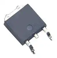


AUIRG4BC30USTRL
IGBT, 23 A, 2.52 V, 100 W, 600 V, TO-263AB, 3 Pins
- Manufacturer: INFINEON
- Product type: Single IGBTs
- No. of Pins: 3Pins
- Power Dissipation: 100W
- Transistor Mounting: Through Hole
- Transistor Case Style: TO-263AB
- Operating Temperature Max: 150°C
- Continuous Collector Current: 23A
- Collector Emitter Voltage Max: 600V
- Automotive Qualification Standard: AEC-Q101
- Collector Emitter Saturation Voltage: 2.52V
| Delivery and price | |
|---|---|
| Units per pack | 1 |
| Price | 0.868 € |
| Current stock | 10+ |
| Lead time | 30 days |
PD - 96335

## **AUTOMOTIVE GRADE**

## AUIRG4BC30U-S AUIRG4BC30U-SL

## UltraFast Speed IGBT

## INSULATED GATE BIPOLAR TRANSISTOR

## **Features**

- UltraFast: Optimized for high operating frequencies 8-40 kHz in hard switching, >200 kHz in resonant mode

- Industry standard D[2] Pak & TO-262 package

- Lead-Free, RoHS Compliant

- Automotive Qualified *

## **Benefits**

- Typical Applications: SMPS, PFC

## **Absolute Maximum Ratings**

**==> picture [211 x 213] intentionally omitted <==**

**----- Start of picture text -----**<br>
C<br>VCES = 600V<br>G VCE(on) typ. = 1.95V<br>E<br>n-channel @VGE = 15V, IC = 12A<br>D [2] Pak TO-262<br>AUIRG4BC30U-S AUIRG4BC30U-SL<br>G C  E<br>Gate Collector Emitter<br>ee<br>**----- End of picture text -----**<br>


Stresses beyond those listed under “Absolute Maximum Ratings” may cause permanent damage to the device. These are stress ratings only; and functional operation of the device at these or any other condition beyond those indicated in the specifications is not implied.Exposure to absolute-maximum-rated conditions for extended periods may affect device reliability. The thermal resistance and power dissipation ratings are measured under board mounted and still air conditions. Ambient temperature (TA) is 25 C, unless otherwise specified

**Parameter Max. Units** VCES ~~a~~ Collector-to-Emitter Breakdown Voltage 600 V IC @ TC = 25°C Continuous Collector Current 23 IC @ TC = 100°C Continuous Collector Current 12 A ~~Se~~ ICM Pulsed Collector Current 92 ILM Clamped Inductive Load Current 92 ———— ae VGE a Gate-to-Emitter Voltage ± 20 V EARV Reverse Voltage Avalanche Energy 10 mJ PD @ TC = 25°C _———————a Maximum Power Dissipation 100 PD @ TC = 100°C Maximum Power Dissipation 42 ~~—— i~~ TJ Operating Junction and -55  to + 150 °C ~~a~~ TSTG Storage Temperature Range **Thermal Resistance Parameter Typ. Max. Units** R θ JC Junction-to-Case ––– 1.2 °C/W R θ JA Junction-to-Ambient,  ( PCB Mounted,steady-state)** ––– 40

- * When mounted on 1" square PCB (FR-4 or G-10 Material ). For recommended footprint and soldering techniques refer  to application note #AN-994.

- Qualification standards can be found at http://www.irf.com/

www.irf.com

1

## AUIRG4BC30U-S/SL

## **Dynamic Electrical Characteristics @ TJ = 25°C (unless otherwise specified)**

|**Parameter**<br>**Min. Typ. Max.**<br>**Units**<br>**Conditions**<br>V(BR)CES<br>Collector-to-Emitter Breakdown Voltage<br>600<br>—<br>—<br>V<br>VGE= 0V, IC= 250µA<br>V(BR)ECS<br>Emitter-to-Collector Breakdown Voltag<br>18<br>—<br>—<br>V<br>VGE= 0V, IC= 1.0A<br>∆V(BR)CES/∆TJ Temperature Coeff. of Breakdown Voltage<br>—<br>0.63<br>—<br>V/°C<br>VGE= 0V, IC= 1.0mA<br>—<br>1.95<br>2.1<br>IC= 12A                          VGE= 15V<br>VCE(ON)<br>Collector-to-Emitter Saturation Voltage<br>—<br>2.52<br>—<br>IC= 23A<br>See Fig.2, 5<br>Se nn SE<br>Se<br>ndde<br>rs<br>Gs ss<br>|<br>|ft<br>a ey|
|---|
|—<br>2.09<br>—<br>IC= 12A , TJ= 150°C<br>VGE(th)<br>Gate Threshold Voltage<br>3.0<br>—<br>6.0<br>VCE= VGE, IC= 250µA<br>∆VGE(th)/∆TJ<br>Temperature Coeff. of Threshold Voltage<br>—<br>-13<br>—<br>mV/°C VCE= VGE, IC= 250µA<br>gfe<br>Forward Transconductance<br>3.1<br>8.6<br>—<br>S<br>VCE=  100V, IC= 12A<br>—<br>—<br>250<br>VGE= 0V, VCE= 600V<br>—<br>—<br>2.0<br>VGE= 0V, VCE= 10V, TJ= 25°C<br>—<br>—<br>1000<br>VGE= 0V, VCE= 600V, TJ= 150°C<br>IGES<br>Gate-to-Emitter Leakage Current<br>—<br>—<br>±100<br>nA<br>VGE= ±20V<br>ICES<br>Zero Gate Voltage Collector Current<br>**Static or Switching Characteristics @ TJ = 25°C (unless otherwise specified)**<br>~~|~~<br>~~| ||~~<br>~~Po~~<br>~~Po~~<br>~~RseG GG~~<br>~~RsGGG~~<br>~~E>~~<br>—a~~ee~~<br>~~es~~<br>~~rs~~ rs rs rs re|
|**Parameter**<br>**Min. Typ. Max.**<br>**Units**<br>**Conditions**|
|Qg<br>Total Gate Charge (turn-on)<br>—<br>50<br>75<br>IC= 12A<br>Qge<br>Gate - Emitter Charge (turn-on)<br>—<br>8.1<br>12<br>nC<br>VCC= 400V<br>See Fig.8<br>Qgc<br>Gate - Collector Charge(turn-on)<br>—<br>18<br>27<br>VGE= 15V<br>td(on)<br>Turn-On Delay Time<br>—<br>17<br>—<br>tr<br>Rise Time<br>—<br>9.6<br>—<br>TJ= 25°C<br>td(off)<br>Turn-Off Delay Time<br>—<br>78<br>120<br>IC= 12A, VCC= 480V<br>tf<br>Fall Time<br>—<br>97<br>150<br>VGE= 15V, RG= 23Ω<br>eeee<br>eees<br>~~ee~~<br>~~ee~~ee<br>~~a~~<br>ee~~ee~~<br>ee~~es~~<br>ee<br>es|
|Eon<br>Turn-On Switching Loss<br>—<br>0.16<br>—<br>Energy losses include "tail"<br>a|
|Eoff<br>Turn-Off Switching Loss<br>—<br>0.20<br>—<br>mJ<br>See Fig. 10, 11, 13, 14<br>Ets<br>Total Switching Loss<br>—<br>0.36<br>0.50<br>td(on)<br>Turn-On Delay Time<br>—<br>20<br>—<br>TJ= 150°C,<br>tr<br>Rise Time<br>—<br>13<br>—<br>IC= 12A, VCC= 480V<br>td(off)<br>Turn-Off Delay Time<br>—<br>180<br>—<br>VGE= 15V, RG= 23Ω<br>tf<br>Fall Time<br>—<br>140<br>—<br>Energy losses include "tail"<br>Ets<br>Total Switching Loss<br>—<br>0.73<br>—<br>mJ<br>See Fig. 13, 14<br>LE<br>Internal Source Inductance<br>—<br>7.5<br>—<br>nH<br>Measured 5mm from package<br>Cies<br>Input Capacitance<br>—<br>1100<br>—<br>VGE= 0V<br>Coes<br>Output Capacitance<br>—<br>73<br>—<br>pF<br>VCC= 30V<br>See Fig.7<br>Cres<br>Reverse Transfer Capacitance<br>—<br>14<br>—<br>ƒ = 1.0MHz<br>a<br>eeee<br>ee<br>a<br>aes<br>ee<br>eeee<br>eG<br>aee<br>es<br>a<br>eeee|


Repetitive rating; VGE = 20V, pulse width limited by max. junction temperature. ( See fig. 13b )

VCC = 80%(VCES), VGE = 20V, L = 10µH, RG = 23 Ω (See fig. 13a)

Pulse width ≤ 80µs; duty factor ≤ 0.1%

Pulse width 5.0µs, single shot.

Repetitive rating; pulse width limited by maximum junction temperature.

www.irf.com

2

## AUIRG4BC30U-S/SL

## **Qualification Information[†]**

|**Qualification Information[†]**|**Qualification Information[†]**|||
|---|---|---|---|
|**Qualification Level**||Automotive<br>(per AEC-Q101)††||
|||Comments:<br>This<br>part<br>number(s)<br>passed<br>Automotive<br>qualification.<br>IR’s<br>Industrial<br>and<br>Consumer<br>qualification<br>level<br>is<br>granted<br>by<br>extension of the higher Automotive level.||
|**Moisture Sensitivity Level**||D2PAK|MSL1|
|||TO-262|N/A|
|**ESD**|Machine Model|Class M4 (+/-450V)<br>AEC-Q101-002||
||Human Body Model|Class  H1C (+/-1750V)<br>AEC-Q101-001||
||Charged Device Model|Class  C5 (+/-1000V)<br>AEC-Q101-005||
|**RoHS Compliant**||Yes||


http://www.irf.com

www.irf.com

3

## AUIRG4BC30U-S/SL

**==> picture [438 x 473] intentionally omitted <==**

**----- Start of picture text -----**<br>
6.0<br>For both: Triangular wave:<br>Duty cycle: 50%<br>5.0 T   = 125°CJ<br>T        = 55°Csink<br>Gate drive as specified<br>a a Power Dissipation = 1.75W Clamp voltage:<br>4.0 80% of rated<br>m A |<br>Square wave:<br>3.0<br>60% of rated<br>         voltage<br>pe<br>2.0 ET L LLL<br>1.0 P oe Ideal diodes TEE PTR SACO<br>| 7"= | ~R |<br>0.0 ee ea:<br>0.1 1 10 100<br>f, Frequency (kHz)<br>Fig. 1  - Typical Load Current vs. Frequency<br>(For square wave, I=IRMS of fundamental; for triangular wave, I=IPK)<br>100 100<br>T  = 25°CJ<br>a T  = 150°CJ EO T  = 150°CJ g o<br>10 10<br>| 2 fey (Annee<br>SSS eet ee Ao T  = 25°C a J aooo<br>ErFIAee eee eee / eee eyPALGey 2 eeetoteee eedegee eee<br>1 1<br>N/E l Ay | | | | |<br>V     = 15VGE V      = 10VCC<br>0.1 Mb oe rurse wore A 0.1 TEsense more A<br>0.1 1 10 5 6 7 8 9 10 11 12<br>V     , Collector-to-Emitter Voltage (V)CE V    , Gate-to-Emitter Voltage (V)GE<br>Load Current (A)<br>I   , Collector-to-Emitter Current (A)C I   , Collector-to-Emitter Current (A)C<br>**----- End of picture text -----**<br>


**Fig. 2** - Typical Output Characteristics

**Fig. 3** - Typical Transfer Characteristics

www.irf.com

4

## AUIRG4BC30U-S/SL

**==> picture [436 x 198] intentionally omitted <==**

**----- Start of picture text -----**<br>
25 3.0<br>I    = 24AC<br>Co E) Pe re<br>20<br>NOL 2.5<br>15<br>SS PTT TNT TTT ae<br>I    = 12AC<br>10<br>PEASE 2.0 ee<br>Pit Te TN oar<br>5<br>I    = 6.0AC<br>pop PN TUT<br>0 EENee ee ee ee A 1.5 TELE Tr [<br>25 50 75 100 125 150 -60 -40 -20 0 20 40 60 80 100 120 140 160<br>T   , Case Temperature (°C)C T  , Junction Temperature (°C)J<br>Maximum DC Collector Current (A CE<br>V     , Collector-to-Emitter Voltage (V)<br>**----- End of picture text -----**<br>


**Fig. 4** - Maximum Collector Current vs.Case Temperature

**Fig. 5** - Collector-to-Emitter  Voltage  vs. Junction Temperature

**==> picture [433 x 197] intentionally omitted <==**

**----- Start of picture text -----**<br>
10<br>po Sep Snaps ssc sp yg<br>a<br>1 |eeeee ee |<br>D = 0.50<br>p e]<br>0.20<br>a 0.10 —_———S——— ee PDM<br>0.1 r r<br>0.05 TT TT t t L<br>1<br>0.020.01       SINGLE PULSE t2<br>(THERMAL RESPONSE)<br>Pe m |e 1. Duty factor D =  t   / t 1 2<br>EL c e e<br>0.01<br>0.00001 0.0001 0.001 0.01 0.1 1 10<br>t   , Rectangular Pulse Duration (sec)1<br>thJC<br>Thermal Response (Z        )<br>**----- End of picture text -----**<br>


**Fig. 6** - Maximum Effective Transient Thermal Impedance, Junction-to-Case

www.irf.com

5

## AUIRG4BC30U-S/SL

**==> picture [208 x 477] intentionally omitted <==**

**----- Start of picture text -----**<br>
2000<br>V      = 0V,         f = 1MHzGE<br>C      = C     + C     ,   C     SHORTEDies         ge         gc         ce<br>C      = C<br>res         gc<br>1600 S| C      = C     + Coes        ce         gc<br>s<br>|<br>1200<br>et lll<br>a eet<br>800 es<br>PNo! TUT TT<br>0<br>400 es<br>ee |<br>PTRTT]<br>0 PE<br>1 10 100<br>V    , Collector-to-Emitter Voltage (V)CE<br>Fig. 7 -  Typical Capacitance vs.<br>Collector-to-Emitter Voltage<br>0.5<br>ivaay—=a80y Pf pp<br>cae”<br>0.4 P| +LA<br>PL  LI<br>ta}<br>0.3 naa 4eeeeee<br>ru KO<br>yf ty<br>0.2 PEE Ey A<br>0 10 20 30 40 50 60<br>R   , Gate Resistance (G Ω )<br>C, Capacitance (pF)<br>Total Switching Losses (mJ)<br>**----- End of picture text -----**<br>


**Fig. 9** - Typical Switching Losses vs. Gate Resistance

**==> picture [196 x 196] intentionally omitted <==**

**----- Start of picture text -----**<br>
20<br>16 Pop | | |<br>12<br>ee<br>Pot LA<br>8<br>a Ae<br>ae<br>4<br>240 eee<br>FE<br>0 pot  tt<br>0 10 20 30 40 50<br>Q  , Total Gate Charge (nC)g<br>GE<br>V     , Gate-to-Emitter Voltage (V)<br>**----- End of picture text -----**<br>


**Fig. 8** - Typical Gate Charge vs. Gate-to-Emitter Voltage

**==> picture [199 x 197] intentionally omitted <==**

**----- Start of picture text -----**<br>
10<br> R      = 23G    Ω TEE<br> V      = 15VGE<br> V      = 480V PEE CC<br>Seeeeeeeeeeeeee<br>PP<br>I    = 24AC<br>1 OEEELLE peeer<br>I    = 12AC<br>PRR tet<br>I    = 6.0AC<br>PEPER EREEEE ee<br>SEPe GRGREDP>—aGaUnenDeen e pee<br>0.1 PTELoeeet<br>-60 -40 -20 0 20 40 60 80 100 120 140 160<br>T  , Junction Temperature (°C)J<br>Total Switching Losses (mJ)<br>**----- End of picture text -----**<br>


**Fig. 10** - Typical Switching Losses vs. Junction Temperature

www.irf.com

6

## AUIRG4BC30U-S/SL

**==> picture [432 x 199] intentionally omitted <==**

**----- Start of picture text -----**<br>
1.6 1000<br>Ω<br>IR =2 Ar T 20V =<br>1.2 IVv_516v= 480V a J ae 100 |0<br>0.8 ee eee 10 [|Z ITSAFE OPERATING AREAQ| (V1<br>EY 401<br>0.4 Aree 1 eyFAREA | ee<br>|<br>0.0 ee eee eee A 0.1 aes|  ev<br>0 10 20 30 1 10 100 1000<br>I   , Collector-to-Emitter Current (A)C V     , Collector-to-Emitter Voltage (V)CE<br>Total Switching Losses (mJ)<br>C<br>I   , Collector-to-Emitter Current (A)<br>**----- End of picture text -----**<br>


**Fig. 11 -** Typical Switching Losses vs. Collector-to-Emitter Current

**Fig. 12** - Turn-Off SOA

www.irf.com

7

## AUIRG4BC30U-S/SL

**==> picture [308 x 99] intentionally omitted <==**

**----- Start of picture text -----**<br>
L D.U.T.<br>V  *<br>C<br>50V 0 - 480v<br>il<br>1000V 480µF<br>960V<br>(0)<br>(2)<br>* Driver same type as D.U.T.; Vc = 80% of Vce(max)<br>* Note: Due to the 50V power supply, pulse width and inductor<br>   will increase to obtain rated Id.<br>**----- End of picture text -----**<br>


**==> picture [264 x 334] intentionally omitted <==**

**----- Start of picture text -----**<br>
IC<br>000 NN<br>L<br>Driver* D.U.T.<br>VC<br>50V<br>1000V<br>T (IE) Ci)<br>o<br>(©)<br>JV<br>90%<br>10%<br>VC<br>90%<br>SS See (ose td(off) 2 a<br>IC 5%10%<br>tr tf<br>t d(on) t=5µs<br>Eon Eoff<br>E   = (E    +E    )ts        on      off<br>**----- End of picture text -----**<br>


www.irf.com

8

## AUIRG4BC30U-S/SL

## www.irf.com

9

## AUIRG4BC30U-S/SL

## TO-262 Package Outline

Dimensions are shown in millimeters (inches)

## TO-262 Part Marking Information

www.irf.com

10

## AUIRG4BC30U-S/SL

Dimensions are shown in millimeters (inches)

**==> picture [343 x 171] intentionally omitted <==**

**----- Start of picture text -----**<br>
TRR<br>1.60 (.063)<br>1.50 (.059)<br>1.60 (.063)<br>4.10 (.161)3.90 (.153) 1.50 (.059) 0.368 (.0145)<br>0.342 (.0135)<br>(=) |<br>FEED DIRECTION 1.85 (.073) 11.60 (.457)<br>1.65 (.065) 11.40 (.449) 24.30 (.957)<br>ZN — eosao 15.42 (.609) £4<br>23.90 (.941)<br>15.22 (.601)<br>TRL<br>eee 10.90 (.429) tt- | 1.75 (.069)1.25 (.049) Tl<br>10.70 (.421) 4.72 (.136)<br>0000 “7 16.10 (.634) J 4.52 (.178)<br>15.90 (.626)<br>FEED DIRECTION<br>**----- End of picture text -----**<br>


**==> picture [334 x 167] intentionally omitted <==**

**----- Start of picture text -----**<br>
13.50 (.532) 27.40 (1.079)<br>; 12.80 (.504) 23.90 (.941) a<br>4<br>330.00 60.00 (2.362)<br>(14.173)       MIN.<br>  MAX.<br>| OO |<br>30.40 (1.197)<br>NOTES : OO a=       MAX.<br>1.   COMFORMS TO EIA-418.2.   CONTROLLING DIMENSION: MILLIMETER. 26.40 (1.039)24.40 (.961) IE 4<br>3.   DIMENSION MEASURED @ HUB.<br>3<br>**----- End of picture text -----**<br>


4.   INCLUDES FLANGE DISTORTION @ OUTER EDGE.

www.irf.com

11

## AUIRG4BC30U-S/SL

## **Ordering Information**

|**Base part number**|**Package Type**|**Standard Pack**|**Standard Pack**|**Complete Part Number**|
|---|---|---|---|---|
|||**Form**|**Quantity**||
|AUIRG4BC30U-SL|TO-262|Tube|**Quantity**<br>50|AUIRG4BC30U-SL|
|AUIRG4BC30U-S|D2Pak|Tube|50|AUIRG4BC30U-S|
|||Tape and Reel Left|800|AUIRG4BC30USTRL|
|||Tape and Reel Right|800|AUIRG4BC30USTRR|


www.irf.com

12

## AUIRG4BC30U-S/SL

Unless specifically designated for the automotive market, International Rectifier Corporation and its subsidiaries (IR) reserve the right to make corrections, modifications, enhancements, improvements, and other changes to its products and services at any time and to discontinue any product or services without notice. Part numbers designated with the “AU” prefix follow automotive industry and / or customer specific requirements with regards to product discontinuance and process change notification. All products are sold subject to IR’s terms and conditions of sale supplied at the time of order acknowledgment.

IR warrants performance of its hardware products to the specifications applicable at the time of sale in accordance with IR’s standard warranty.  Testing and other quality control techniques are used to the extent IR deems necessary to support this warranty. Except where mandated by government requirements, testing of all parameters of each product is not necessarily performed.

IR assumes no liability for applications assistance or customer product design. Customers are responsible for their products and applications using IR components. To minimize the risks with customer products and applications, customers should provide adequate design and operating safeguards.

Reproduction of IR information in IR data books or data sheets is permissible only if reproduction is without alteration and is accompanied by all associated warranties, conditions, limitations, and notices.  Reproduction of this information with alterations is an unfair and deceptive business practice.  IR is not responsible or liable for such altered documentation.  Information of third parties may be subject to additional restrictions.

Resale of IR products or serviced with statements different from or beyond the parameters stated by IR for that product or service voids all express and any implied warranties for the associated IR product or service and is an unfair and deceptive business practice.  IR is not responsible or liable for any such statements.

IR products are not designed, intended, or authorized for use as components in systems intended for surgical implant into the body, or in other applications intended to support or sustain life, or in any other application in which the failure of the IR product could create a situation where personal injury or death may occur.  Should Buyer purchase or use IR products for any such unintended or unauthorized application, Buyer shall indemnify and hold International Rectifier and its officers, employees, subsidiaries, affiliates, and distributors harmless against all claims, costs, damages, and expenses, and reasonable attorney fees arising out of, directly or indirectly, any claim of personal injury or death associated with such unintended or unauthorized use, even if such claim alleges that IR was negligent regarding the design or manufacture of the product.

IR products are neither designed nor intended for use in military/aerospace applications or environments unless the IR products are specifically designated by IR as military-grade or “enhanced plastic.”  Only products designated by IR as military-grade meet military specifications.  Buyers acknowledge and agree that any such use of IR products which IR has not designated as military-grade is solely at the Buyer’s risk, and that they are solely responsible for compliance with all legal and regulatory requirements in connection with such use.

IR products are neither designed nor intended for use in automotive applications or environments unless the specific IR products are designated by IR as compliant with ISO/TS 16949 requirements and bear a part number including the designation “AU”.  Buyers acknowledge and agree that, if they use any non-designated products in automotive applications, IR will not be responsible for any failure to meet such requirements

For technical support, please contact IR’s Technical Assistance Center

http://www.irf.com/technical-info/

## **WORLD HEADQUARTERS:**

233 Kansas St., El Segundo, California 90245

Tel: (310) 252-7105

www.irf.com

13
Updated at February 9, 2023
Infineon Technologies is a globally recognized leader in semiconductor solutions, renowned for driving innovation in power management, energy efficiency, and modern mobility. With a strong legacy of engineering excellence, the company provides highly reliable components designed to meet the rigorous demands of industrial, automotive, and advanced commercial applications. The core of our Infineon portfolio is centered on their industry-leading discrete semiconductors. We offer an extensive selection of single and dual MOSFETs, alongside a robust range of single IGBTs and advanced IGBT modules. These flagship power transistors are essential for high-efficiency power conversion and motor control, providing engineers with superior thermal performance and minimized switching losses. Beyond advanced field-effect transistors, the selection includes a comprehensive array of diodes and rectifiers, heavily featuring Schottky diodes, as well as fast-recovery and RF/PIN diodes. This power foundation is further supported by bipolar transistors, intelligent power modules, and thyristor SCR modules, delivering the critical building blocks required for complex power system designs. To support broader system integration, the portfolio also encompasses specialized solutions such as solid-state relays, AC/DC LED driver ICs, and Bluetooth communications modules. From high-power industrial rectifiers to wireless connectivity adapters, Infineon equips designers with the precision components needed to build efficient, scalable, and fully connected electronic systems.
About Novapart
Novapart is a B2B electronic component broker specialising in stock shortages and cost reduction. We source hard-to-find parts and identify compliant alternatives across a catalogue of 410,000+ components from 500+ manufacturers.
Learn more →Stock Shortage Specialist
When a component is unavailable, discontinued or has an unacceptable lead time, we tap into our network of vetted European and Asian distributors to source what you need — without compromising on quality or traceability.
Request a quote →Compliant Alternatives
We identify pin-to-pin, electrically equivalent substitutes that meet the same certifications (RoHS, AEC-Q100, REACH) as your original specification — validated against datasheets, not just part numbers. Often at a lower cost.
BOM Analysis service →