


AUIRF7304Q
Dual MOSFET, P Channel, 20 V, 4.3 A
- Manufacturer: INFINEON
- Product type: Dual MOSFETs
- Transistor Polarity:Dual P Channel; Continuous Drain Current Id:-4.3A; Drain Source Voltage Vds:-20V; On Resistance Rds(on):0.09ohm; Rds(on) Test Voltage Vgs:-4.5V; Threshold Voltage Vgs:-7
- No. of Pins: 8Pins
- Channel Type: P Channel
- Product Range: -
- Qualification: AEC-Q101
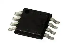
- Transistor Case Style: SOIC
- Operating Temperature Max: 150°C
- Power Dissipation N Channel: -
- Power Dissipation P Channel: 2W
- Drain Source Voltage Vds N Channel: -
- Drain Source Voltage Vds P Channel: 20V
- Continuous Drain Current Id N Channel: -
- Continuous Drain Current Id P Channel: 4.3A
- Drain Source On State Resistance N Channel: -
- Drain Source On State Resistance P Channel: 0.09ohm
| Delivery and price | |
|---|---|
| Units per pack | 5000 |
| Price | 0.491 € |
| Current stock | 10+ |
| Lead time | 30 days |
## **AUTOMOTIVE GRADE**

## **Features**

Advanced Planar Technology Low On-Resistance Dual P Channel MOSFET

Dynamic dV/dT Rating Logic Level 150°C Operating Temperature Fast Switching Lead-Free, RoHS Compliant Automotive Qualified*

**==> picture [226 x 67] intentionally omitted <==**

**----- Start of picture text -----**<br>
S1 1 8 D1 V -20V<br>(BR)DSS<br>G1 2 7 D1<br>S2 3 6 D2 R  max. 0.090 Ω<br>DS(on)<br>G2 ait 4 5 D2<br>“nape<br>Top View ID -4.3A<br>**----- End of picture text -----**<br>


## **Description**

Specifically designed for Automotive applications, this cellular design of HEXFET® Power MOSFETs utilizes the latest processing techniques to achieve low on-resistance per silicon area. This benefit combined with the fast switching speed and ruggedized device design that HEXFET power MOSFETs are well known for, provides the designer with an extremely efficient and reliable device for use in Automotive and a wide variety of other applications.

**==> picture [58 x 21] intentionally omitted <==**

**----- Start of picture text -----**<br>
SO-8<br>AUIRF7304Q<br>**----- End of picture text -----**<br>


## **Absolute Maximum Ratings**

|Stresses beyond those listed under “Absolute Maximum Ratings” may cause permanent damage to the device.   These|
|---|
|are stress ratings only; and functional operation of the device at these or any other condition beyond those indicated|
|in the specifications is not implied. Exposure to absolute-maximum-rated conditions for extended periods may affect|
|device reliability. The thermal resistance and power dissipation ratings are measured under board mounted and still air|
|conditions. Ambient temperature (TA) is 25°C, unless otherwise specified.|
|**Parameter**<br>**Units**<br>ID@ TA= 25°C<br>10 Sec. Pulsed Drain Current, VGS@ -4.5V<br>ID @ TA= 25°C<br>Continuous Drain Current, VGS@ -4.5V<br>A<br>ID@ TA= 70°C<br>Continuous Drain Current, VGS@ -4.5V<br>IDM<br>Pulsed Drain Current<br>PD@TA= 25°C<br>Power Dissipation<br>W<br>Linear Derating Factor<br>W/°C<br>VGS<br>Gate-to-Source Voltage<br>V<br>dv/dt<br>Peak Diode Recovery dv/dt<br>V/ns<br>TJ<br>Operating Junction and<br>°C<br>TSTG<br>Storage Temperature Range<br>**Max.**<br>-4.7<br>-4.3<br>-17<br>-3.4<br>-55  to + 150<br>2.0<br>0.016<br>-5.0<br>± 12<br>~~===.~~<br>~~To~~<br>~~i~~<br>~~oo~~<br>~~OO~~<br>~~oes~~<br>~~oT~~<br>~~EET~~<br>~~LO~~<br>~~a~~<br>~~ee~~<br>~~ee ee~~|
|**Thermal Resistance**|
|**Parameter**<br>**Typ.**<br>**Max.**<br>**Units**<br>RθJA<br>Junction-to-Ambient<br>–––<br>62.5<br>°C/W<br>~~ee~~|


HEXFET[®] is a registered trademark of International Rectifier.

***** Qualification standards can be found at http://www.irf.com/

www.irf.com

1

**Static Electrical Characteristics @ TJ = 25°C (unless otherwise specified)**

||**Parameter**<br>**Min. Typ. Max. Units**<br>**Conditions**||
|---|---|---|
|V(BR)DSS<br>ΔV(BR)DSS/ΔTJ<br>VGS(th)<br>gfs<br>IDSS<br>IGSS<br>RDS(on)|Drain-to-Source Breakdown Voltage<br>-20<br>–––<br>–––<br>V<br>Breakdown Voltage Temp. Coefficient<br>–––<br>-0.012<br>–––<br>V/°C<br>–––<br>–––<br>0.090<br>–––<br>–––<br>0.140<br>Gate Threshold Voltage<br>-0.70<br>–––<br>-1.5<br>V<br>Forward Transconductance<br>4.0<br>–––<br>–––<br>S<br>Drain-to-Source Leakage Current<br>–––<br>–––<br>-1.0<br>–––<br>–––<br>-25<br>Gate-to-Source Forward Leakage<br>–––<br>–––<br>-100<br>Gate-to-Source Reverse Leakage<br>–––<br>–––<br>100<br>nA<br>μA<br>VDS= -16V, VGS= 0V<br>VDS= -16V, VGS= 0V, TJ= 125°C<br>VGS= 12V<br>VGS= 0V, ID= -250μA<br>Reference to 25°C, ID= -1mA<br>VGS= -4.5V, ID= -2.2A<br>Static Drain-to-Source On-Resistance<br>Ω<br>VGS= -2.7V,ID= -1.8A<br>VDS= VGS, ID= -250μA<br>VDS= -16V, ID= -2.2A<br>VGS= -12V<br>~~GO~~<br>~~Gn~~<br>~~QO QO~~<br>~~es~~<br>~~||~~<br>~~es~~<br>~~GS QO~~<br>~~Gn~~<br>~~GN QO OO~~<br>~~—————~~<br>~~aesa~~||
|**Dynamic  Electrical Characteristics @ TJ = 25°C(unless otherwise specified)**|||
|Qg<br>Qgs<br>Qgd<br>td(on)|**Parameter**<br>**Min. Typ. Max. Units**<br>Total Gate Charge<br>–––<br>–––<br>22<br>Gate-to-Source Charge<br>–––<br>–––<br>3.3<br>Gate-to-Drain("Miller")Charge<br>–––<br>–––<br>9.0<br>Turn-On DelayTime<br>–––<br>8.4<br>–––<br>VGS= -4.5V, See Fig. 6 & 12<br>VDS= -16V<br>VDD= -10V<br>nC<br>**Conditions**<br>ID= -2.2A<br>~~ss~~<br>~~GG~~<br>~~ee~~<br>~~es~~<br>~~ee~~<br>~~es~~<br>~~ee ee~~<br>~~ee~~<br>~~@~~<br>~~ee~~||
|tr<br>td(off)|Rise Time<br>–––<br>26<br>–––<br>Turn-Off DelayTime<br>–––<br>51<br>–––<br>ID= -2.2A<br>RG= 6.0Ω<br>ns<br>~~ee~~<br>~~ee~~||
|tf|Fall Time<br>–––<br>33<br>–––<br>RD= 4.5Ω, See Fig. 10<br>~~ee~~<br>®||
|LD<br>LS<br>Ciss<br>Coss<br>Crss|S<br>D<br>G<br>Internal Drain Inductance<br>–––<br>4.0<br>–––<br>Between lead,<br>nH<br>6mm (0.25in.)<br>Internal Source Inductance<br>–––<br>6.0<br>–––<br>from package<br>and center of die contact<br>Input Capacitance<br>–––<br>610<br>–––<br>Output Capacitance<br>–––<br>310<br>–––<br>Reverse Transfer Capacitance<br>–––<br>170<br>–––<br>VGS= 0V<br>VDS= -15V<br>ƒ= 1.0MHz, See Fig. 5<br>pF<br>~~ra~~<br>~~|~~<br>~~ee~~<br>~~es~~<br>~~ee~~<br>~~es~~<br>~~ee~~||
|**Diode Characteristics**|||
||**Parameter**<br>**Min. Typ. Max. Units**<br>**Conditions**||
|IS<br>ISM|S<br>D<br>G<br>Continuous Source Current<br>(BodyDiode)<br>Pulsed Source Current<br>(BodyDiode)<br>-17<br>–––<br>–––<br>–––<br>–––<br>-2.5<br>A<br>integral reverse<br>p-njunction diode.<br>MOSFET symbol<br>showing  the<br>~~|~~||
|VSD<br>trr<br>Qrr<br>ton|Diode Forward Voltage<br>–––<br>–––<br>-1.0<br>V<br>Reverse RecoveryTime<br>–––<br>56<br>84<br>ns<br>TJ= 25°C,IF= -2.2A<br>Reverse RecoveryCharge<br>–––<br>71<br>110<br>nC<br>di/dt = 100A/μs<br>Forward Turn-On Time<br>Intrinsic turn-on time is negligible (turn-on is dominated by LS+LD)<br>TJ= 25°C, IS= -1.8A, VGS= 0V<br>~~Gn~~<br>~~GN~~<br>~~rr~~<br>~~ee~~<br>~~°~~<br>~~a~~||


Pulse width ≤ 300μs; duty cycle ≤ 2%.

ISD ≤ ≤− ≤ ≤

Starting TJ = 25°C, RG = 25 Ω , IAS = -2.2A.

When mounted  on 1 inch square copper board,  t<10 sec.

www.irf.com

2

## **Qualification Information†**

|**Qualification Information†**<br>**†**|**Qualification Information†**<br>**†**|||
|---|---|---|---|
|**Qualification Level**||Automotive<br>(per AEC-Q101)<br>††||
|||Comments: This part number(s) passed Automotive qualification. IR’s<br>Industrial and Consumer qualification level is granted by extension of the<br>higher Automotive level.||
|**Moisture Sensitivity Level**||SO-8|MSL1|
|**ESD**|Machine Model|Class M1B (+/- 100V)<br>†††<br>AEC-Q101-002||
||Human Body Model|Class H0 (+/- 250V)<br>†††<br>AEC-Q101-001||
||Charged Device<br>Model|Class C5 (+/- 2000V)†††<br>AEC-Q101-005||
|**RoHS Compliant**||Yes||


www.irf.com

3

**==> picture [439 x 473] intentionally omitted <==**

**----- Start of picture text -----**<br>
100 100<br> TOP         - 7.5V  TOP         - 7.5V<br>- 5.0V - 5.0V<br>- 4.0V or AA oo - 4.0V oe eo<br>                 - 3.5V                  - 3.0V a 7 el                  - 3.5V                  - 3.0V |<br>- 2.5V EE - 2.5V A |<br>                 - 2.0V                  - 2.0V<br> BOTTOM - 1.5V Y/Zc a  BOTTOM - 1.5V a<br>10 10<br>PaAG cI<br>an Ad ae pL ffffon<br>1 1<br>-1.5V<br>| \  -1.5V a) //4y Ae<br> 20μs PULSE WIDTH<br>0.1 AVAYe  T   = 25°CJ rues mone A 0.1 Vd y Pi  T   = 150°CJ<br>0.01 0.1 1 10 100 0.01 0.1 1 10 100<br>-V     , Drain-to-Source Voltage (V)DS -V     , Drain-to-Source Voltage (V)DS<br>Fig 1. Typical Output Characteristics Fig 2. Typical Output Characteristics<br>100 BSS ES SSS 2.0 PTT<br>ee ee ee ee ee ee<br>ae S———- 1.5 OO UR GR GR GR GU GR GR GRURGE<br>T  = 25°CJ T  = 150°CJ<br>10<br>| yee PEELE EP<br>Sar 4eaeseseses 1.0 ee ttl<br>PA LS ar<br>4 eT ELE<br>1 Yjti| | | ft | cn<br>f= 0.5 PPE EEE<br>a2eeee eee eee SE<br> V     = -15V DS<br>0.11.5 PTTPETA 2.0 2.5 3.0 saatusewors 3.5 couspurse 4.0 4.5 wor 5.0A 0.0-60 PPE -40 -20 0 20 40 EE 60 80 100 bes 120 140 160<br>-V     , Gate-to-Source Voltage (V)GS T   , Junction Temperature (°C)J<br>D D<br>-I   , Drain-to-Source Current (A) -I   , Drain-to-Source Current (A)<br>(Normalized)<br>D<br>-I   , Drain-to-Source Current (A)<br>DS(on)<br>R           ,  Drain-to-Source On Resistance<br>**----- End of picture text -----**<br>


www.irf.com

4

**==> picture [443 x 467] intentionally omitted <==**

**----- Start of picture text -----**<br>
1500 10<br>V      = 0V,         f = 1MHzGS  I    = -2.2AD<br>C      = C     + C     ,   C     SHORTEDiss         gs         gd         ds  V     =   DS -16V<br>C      = Crss         gd<br>C      = C     + C oss        ds         gd 8<br>\ [ot ft<br>s<br>1000 Nt) Fee<br>6<br>ss<br>NO AU<br>Null l Saaeeny ane<br>ss 4<br>A el eee<br>500<br>2<br>EN a) ee oe ee  Ae<br>0 TF A 0 rere     SEE FIGURE 12<br>1 10 100 0 5 10 15 20 25<br>-V     , Drain-to-Source Voltage (V)DS Q   , Total Gate Charge (nC)G<br>Fig 5. Typical Capacitance Vs. Fig 6. Typical Gate Charge Vs.<br>Drain-to-Source Voltage Gate-to-Source Voltage<br>100  100<br>OPERATION IN THIS AREA LIMITED<br>SSS SSS SS SS =n: BY RDS(on)<br>10 aso|__| T    __|_esep_ J = 150°C achEen ellth<br>T  = 25J °C<br>Sa<br> 10<br>+ 2 a e eAi<br>V ff + J ——— a ee eee 1ms<br>1<br>ap ESSER CEH<br>ael<br>——  a/.eeee SSS<br>my ew eee eee eee  T  TAJ = 25  C = 150  C ° ° N 10ms<br>0.1 al A  1  Single Pulse all<br>0.3 0.6 0.9 1.2 1.5  1  10  100<br>-V     , Source-to-Drain Voltage (V)SD -V     , Drain-to-Source Voltage (V)DS<br>C, Capacitance (pF)<br>GS<br>-V     , Gate-to-Source Voltage (V)<br>SD I   , Drain Current (A) D-<br>-I     , Reverse Drain Current (A)<br>**----- End of picture text -----**<br>


www.irf.com

5

**==> picture [400 x 199] intentionally omitted <==**

**----- Start of picture text -----**<br>
5.0<br>-<br>+<br>4.0 ~GREEEEEEe<br>PP $ 48  1<br>Sayracor ≤ 0.1 %<br>3.0 PtP [PNET] V<br>HERP Fig 10a. Switching Time Test Circuit<br>2.0<br>VDS<br>PEN 90% —<br>1.0 Pt PT TT TT TN x<br>pi titi titty<br>0.0 pit iT  tt 10% X<br>25 50 75 100 125 150<br>T   , Case TemperatureC (  C)° VGS<br>td(on) tr td(off) tf<br>D<br>-I   , Drain Current (A)<br>**----- End of picture text -----**<br>


**==> picture [426 x 194] intentionally omitted <==**

**----- Start of picture text -----**<br>
 100<br>D = 0.50<br>nena GREE, cae ee<br>0.20 STeee<br> 10 ee eerwoes<br>0.10<br>0.05<br>eee aati menses 2: ete ee ee<br>0.02<br>PDM<br>0.01<br> 1 = S SINGLE PULSE oTLe CU LL t1<br>(THERMAL RESPONSE) t2<br>aa eeee eeee eeeeee 1. Duty factor D = Notes: t   / t 1 2<br>a 2. Peak T J = P DM x  Z thJA + TA<br>0.1<br>0.0001 0.001 0.01 0.1  1  10  100<br>t  , Rectangular Pulse Duration (sec)1<br>thJA<br>(Z        )<br>Thermal Response<br>**----- End of picture text -----**<br>


www.irf.com

6

**==> picture [379 x 158] intentionally omitted <==**

**----- Start of picture text -----**<br>
Current Regulator<br>Same Type as D.U.T.<br>50K Ω<br>12V .2 μ F<br>QG .3 μ F<br>QGS QGD ne i D.U.T. +-VDS<br>VGS<br>V Me G -3mA (ay<br>or al IG ID<br>Charge Current Sampling Resistors<br>**----- End of picture text -----**<br>


www.irf.com

7

**==> picture [271 x 451] intentionally omitted <==**

**----- Start of picture text -----**<br>
D.U.T + Circuit Layout Considerations<br>™    •  Low Stray Inductance<br>®  •   Ground Plane<br> •   Low Leakage Inductance<br>| - Current Transformer<br>+<br>- - +<br>0<br>kK<br>®<br>Re •   dv/dt controlled by Rg +<br>•   -<br>CO •   D.U.T. - Device Under Test<br>‘ > Isp controlled by Duty Factor "D"<br>* Reverse Polarity for P-Channel<br>** Use P-Channel Driver for P-Channel Measurements<br>® Driver Gate Drive<br>P.W.<br>Period D =<br>P.W. | Period _ t<br>t<br>@ D.U.T. ISD Waveform<br>Reverse<br>Recovery Body Diode Forward<br>Current "\ Current di/dt a<br>©) D.U.T. VDS Waveform<br>Diode Recoverydv/dt \ F<br>[,<br>Re-Applied<br>Voltage Body Diode  Forward Drop<br>® Inductor Curent<br>a<br>Ripple  ≤ 5% ]<br>**----- End of picture text -----**<br>


www.irf.com

8

**SO-8 Package Outline** Dimensions are shown in millimeters (inches)

## **SO-8 Part Marking**

**==> picture [185 x 419] intentionally omitted <==**

**----- Start of picture text -----**<br>
|__|| 0 | coveiso || 1908cov8 || o19480 [ozs[500 ||<br>|e | 050 Basic | 127 BASIC |<br>lyfefe te fe |<br>7 i Kx 45 °<br>y £ —t<br>L 0 4) ~ La x axe +<br>FOOTPRINT<br>Y14.5M-1994. 8X.0.72 [,028]<br>_ [~<br>redo<br>eei25)“ iFO e e| i<br>TO<br>3X 1.27 [050] — = | 8X 1.78<br>D A T E COD E<br>5<br>=P| = I) WNE K O @<br>TéaR A YWW? | M A RKING COD E<br>=F , | (Per Marking<br>- i F 7304Q z<br>**----- End of picture text -----**<br>


www.irf.com

9

## **SO-8 Tape and Reel**

Dimensions are shown in millimeters (inches)

**==> picture [72 x 5] intentionally omitted <==**

**----- Start of picture text -----**<br>
TERMINAL NUMBER 1<br>**----- End of picture text -----**<br>


**==> picture [239 x 97] intentionally omitted <==**

**----- Start of picture text -----**<br>
12.3 ( .484 )<br>11.7 ( .461 )<br>8.1 ( .318 )<br>7.9 ( .312 ) FEED DIRECTION<br>TT<br>**----- End of picture text -----**<br>


NOTES:

1.   CONTROLLING DIMENSION : MILLIMETER.

2.   ALL DIMENSIONS ARE SHOWN IN MILLIMETERS(INCHES). 3.   OUTLINE CONFORMS TO EIA-481 & EIA-541.

**==> picture [252 x 152] intentionally omitted <==**

**----- Start of picture text -----**<br>
 330.00<br>(12.992)<br>  MAX.<br>ID |<br>[ V Y<br>14.40 ( .566 )<br>12.40 ( .488 )<br>**----- End of picture text -----**<br>


NOTES :

1. CONTROLLING DIMENSION : MILLIMETER.

2. OUTLINE CONFORMS TO EIA-481 & EIA-541.

www.irf.com

10

## **Ordering Information**

|**Base part**<br>**number**|**Package Type**|**Standard Pack**|**Standard Pack**|**Complete Part Number**|
|---|---|---|---|---|
|||**Form**|**Quantity**||
|AUIRF7304Q|SO-8|Tube|95|AUIRF7304Q|
|||Tape and Reel|2500|AUIRF7304QTR|


www.irf.com

11

Unless specifically designated for the automotive market, International Rectifier Corporation and its subsidiaries (IR) reserve the right to make corrections, modifications, enhancements, improvements, and other changes to its products and services at any time and to discontinue any product or services without notice. Part numbers designated with the “AU” prefix follow automotive industry and / or customer specific requirements with regards to product discontinuance and process change notification. All products are sold subject to IR’s terms and conditions of sale supplied at the time of order acknowledgment.

IR warrants performance of its hardware products to the specifications applicable at the time of sale in accordance with IR’s standard warranty.  Testing and other quality control techniques are used to the extent IR deems necessary to support this warranty. Except where mandated by government requirements, testing of all parameters of each product is not necessarily performed.

IR assumes no liability for applications assistance or customer product design. Customers are responsible for their products and applications using IR components. To minimize the risks with customer products and applications, customers should provide adequate design and operating safeguards.

Reproduction of IR information in IR data books or data sheets is permissible only if reproduction is without alteration and is accompanied by all associated warranties, conditions, limitations, and notices.  Reproduction of this information with alterations is an unfair and deceptive business practice.  IR is not responsible or liable for such altered documentation.  Information of third parties may be subject to additional restrictions.

Resale of IR products or serviced with statements different from or beyond the parameters stated by IR for that product or service voids all express and any implied warranties for the associated IR product or service and is an unfair and deceptive business practice.  IR is not responsible or liable for any such statements.

IR products are not designed, intended, or authorized for use as components in systems intended for surgical implant into the body, or in other applications intended to support or sustain life, or in any other application in which the failure of the IR product could create a situation where personal injury or death may occur.  Should Buyer purchase or use IR products for any such unintended or unauthorized application, Buyer shall indemnify and hold International Rectifier and its officers, employees, subsidiaries, affiliates, and distributors harmless against all claims, costs, damages, and expenses, and reasonable attorney fees arising out of, directly or indirectly, any claim of personal injury or death associated with such unintended or unauthorized use, even if such claim alleges that IR was negligent regarding the design or manufacture of the product.

IR products are neither designed nor intended for use in military/aerospace applications or environments unless the IR products are specifically designated by IR as military-grade or “enhanced plastic.”  Only products designated by IR as military-grade meet military specifications.  Buyers acknowledge and agree that any such use of IR products which IR has not designated as military-grade is solely at the Buyer’s risk, and that they are solely responsible for compliance with all legal and regulatory requirements in connection with such use.

IR products are neither designed nor intended for use in automotive applications or environments unless the specific IR products are designated by IR as compliant with ISO/TS 16949 requirements and bear a part number including the designation “AU”.  Buyers acknowledge and agree that, if they use any non-designated products in automotive applications, IR will not be responsible for any failure to meet such requirements.

For technical support, please contact IR’s Technical Assistance Center http://www.irf.com/technical-info/

## **WORLD HEADQUARTERS:**

101 N. Sepulveda Blvd., El Segundo, California 90245 Tel: (310) 252-7105

www.irf.com

12
Updated at June 9, 2026
Infineon Technologies is a globally recognized leader in semiconductor solutions, renowned for driving innovation in power management, energy efficiency, and modern mobility. With a strong legacy of engineering excellence, the company provides highly reliable components designed to meet the rigorous demands of industrial, automotive, and advanced commercial applications. The core of our Infineon portfolio is centered on their industry-leading discrete semiconductors. We offer an extensive selection of single and dual MOSFETs, alongside a robust range of single IGBTs and advanced IGBT modules. These flagship power transistors are essential for high-efficiency power conversion and motor control, providing engineers with superior thermal performance and minimized switching losses. Beyond advanced field-effect transistors, the selection includes a comprehensive array of diodes and rectifiers, heavily featuring Schottky diodes, as well as fast-recovery and RF/PIN diodes. This power foundation is further supported by bipolar transistors, intelligent power modules, and thyristor SCR modules, delivering the critical building blocks required for complex power system designs. To support broader system integration, the portfolio also encompasses specialized solutions such as solid-state relays, AC/DC LED driver ICs, and Bluetooth communications modules. From high-power industrial rectifiers to wireless connectivity adapters, Infineon equips designers with the precision components needed to build efficient, scalable, and fully connected electronic systems.
About Novapart
Novapart is a B2B electronic component broker specialising in stock shortages and cost reduction. We source hard-to-find parts and identify compliant alternatives across a catalogue of 410,000+ components from 500+ manufacturers.
Learn more →Stock Shortage Specialist
When a component is unavailable, discontinued or has an unacceptable lead time, we tap into our network of vetted European and Asian distributors to source what you need — without compromising on quality or traceability.
Request a quote →Compliant Alternatives
We identify pin-to-pin, electrically equivalent substitutes that meet the same certifications (RoHS, AEC-Q100, REACH) as your original specification — validated against datasheets, not just part numbers. Often at a lower cost.
BOM Analysis service →