
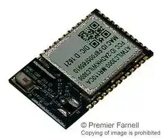


ATWILC3000-MR110CA
Wireless LAN Module, 2.472 GHz, SPI, SDIO, Wireless Connectivity
- Manufacturer: MICROCHIP
- Product type: WLAN Modules & USB Adaptors
- Frequency RF:2.472GHz; Module Interface:SPI, SDIO; Module Applications:Wireless Connectivity; Product Range:-; SVHC:No SVHC (15-Jan-2018)
- SVHC: No SVHC (04-Feb-2026)
- Frequency RF: 2.472GHz
- Product Range: -
- Module Interface: SPI, SDIO
- Module Applications: Wireless Connectivity
| Delivery and price | |
|---|---|
| Units per pack | 250 |
| Price | 9.05 € |
| Current stock | 100+ |
| Lead time | 30 days |
**==> picture [39 x 54] intentionally omitted <==**

## **ATWILC3000-MR110CA**

## **IEEE 802.11 b/g/n Link Controller Module with Integrated Bluetooth® 4.0**

## **Description**

The ATWILC3000-MR110CA module is an IEEE 802.11 b/g/n RF/Baseband/Medium Access Control (MAC) link controller and Bluetooth 4.0 compliant module[(1)] , optimized for low power mobile applications. This module supports single stream 1x1 IEEE 802.11n mode providing up to 72 Mbps PHY rate. The ATWILC3000-MR110CA module features small form factor when integrating Power Amplifier (PA), LowNoise Amplifier (LNA), Transmit/Receive switch, Power Management, and chip Antenna. This module offers very low power consumption while simultaneously providing high performance. This module contains all circuitry required including a chip antenna, 26 MHz crystal, and PMU circuitry. The ATWILC3000-MR110CA module requires a 32.768 kHz clock for sleep operation.

The ATWILC3000-MR110CA module utilizes highly optimized IEEE 802.11 Bluetooth coexistence protocols, and provides Serial Peripheral Interface (SPI) and Secure Digital Input Output (SDIO) for interfacing with the host controller.

## **Features**

## **IEEE 802.11:**

- IEEE 802.11 b/g/n RF/PHY/MAC SOC

- IEEE 802.11 b/g/n (1x1) for up to 72 Mbps PHY rate

- Single spatial stream in 2.4 GHz ISM band

- Integrated PA and T/R switch

- Integrated chip antenna

- Superior sensitivity and range via advanced PHY signal processing

- Advanced equalization and channel estimation

- Advanced carrier and timing synchronization

- Wi-Fi Direct® and Soft-AP support

- Supports IEEE 802.11 WEP, WPA, WPA2 and WPA2 Enterprise security

- Superior MAC throughput through hardware accelerated two-level A-MSDU/A-MPDU frame aggregation and block acknowledgement

- On-chip memory management engine to reduce host load

- SPI and SDIO host interfaces

- Operating temperature range from -40°C to +85°C

- Wi-Fi Alliance[®] certified for connectivity and optimizations

   - ID: WFA72428

## **Bluetooth:**

- Bluetooth 4.0(Basic Rate, Enhanced Data Rate and BLE)[(1)]

**Datasheet**

DS70005327A-page 1

© 2017 Microchip Technology Inc.

**ATWILC3000-MR110CA**

- Frequency hopping

- Host Control Interface (HCI) through high speed UART

- Integrated PA and T/R switch

- Superior sensitivity and range

- BT SIG QDID - 99659[(1)]

## **Note:**

1. BT SIG QDID qualification is for BLE only

**Datasheet**

DS70005327A-page 2

© 2017 Microchip Technology Inc.

## **Table of Contents**

|Description.......................................................................................................................1|Description.......................................................................................................................1|
|---|---|
|Features.......................................................................................................................... 1||
|1. Ordering Information and Module Marking................................................................6||
|2. Block|Diagram........................................................................................................... 7|
|3. Pinout and Package Information............................................................................... 8||
|3.1.|Package Description...................................................................................................................11|
|4. Electrical Characteristics......................................................................................... 12||
|4.1.|Absolute Maximum Ratings........................................................................................................12|
|4.2.|Recommended Operating Conditions........................................................................................ 12|
|4.3.|DC Characteristics..................................................................................................................... 13|
|4.4.|IEEE 802.11 b/g/n Radio Performance...................................................................................... 13|
|4.5.|Bluetooth Radio Performance.................................................................................................... 16|
|4.6.|Timing Characteristics................................................................................................................17|
|5. Power Management................................................................................................ 23||
|5.1.|Device States............................................................................................................................. 23|
|5.2.|Controlling Device States...........................................................................................................23|
|5.3.|Power-Up/Down Sequence........................................................................................................24|
|5.4.|Digital I/O Pin Behavior During Power-Up Sequences...............................................................25|
|6. Clocking...................................................................................................................27||
|6.1.|Low-Power Clock....................................................................................................................... 27|
|7. CPU and Memory Subsystem................................................................................. 28||
|7.1.|Processor................................................................................................................................... 28|
|7.2.|Memory Subsystem....................................................................................................................28|
|7.3.|Nonvolatile Memory....................................................................................................................28|
|8. WLAN Subsystem................................................................................................... 30||
|8.1.|MAC........................................................................................................................................... 30|
|8.2.|PHY............................................................................................................................................31|
|8.3.|Radio..........................................................................................................................................31|
|9. Bluetooth Subsystem...............................................................................................33||
|9.1.|Bluetooth 4.0.............................................................................................................................. 33|
|9.2.|Features..................................................................................................................................... 33|
|10. External Interfaces...................................................................................................34||
|10.1.|Interfacing with the Host Microcontroller.................................................................................... 34|
|10.2.|SDIO Slave Interface..................................................................................................................35|
|10.3.|SPI Slave Interface.....................................................................................................................36|


**Datasheet**

DS70005327A-page 3

© 2017 Microchip Technology Inc.

**ATWILC3000-MR110CA**

|10.4. I2C Slave Interface..................................................................................................................... 37|
|---|
|10.5. UART Debug Interface...............................................................................................................37|
|10.6. SPI Master Interface...................................................................................................................38|
|10.7. PCM Interface............................................................................................................................ 38|
|10.8. GPIOs.........................................................................................................................................39|
|10.9. Internal Pull up Resistors........................................................................................................... 39|
|11. Application Reference Design................................................................................. 40|
|11.1.<br>Host Interface - SPI....................................................................................................................40|
|11.2.<br>Host Interface - SDIO ................................................................................................................41|
|12. Module Outline Drawings........................................................................................ 43|
|13. Design Consideration.............................................................................................. 44|
|13.1. Module Placement and Routing Guidelines............................................................................... 44|
|13.2. Antenna Performance................................................................................................................ 45|
|14. Reflow Profile Information....................................................................................... 49|
|14.1. Storage Condition.......................................................................................................................49|
|14.2. Solder Paste...............................................................................................................................49|
|14.3. Stencil Design............................................................................................................................ 49|
|14.4. Baking Conditions...................................................................................................................... 49|
|14.5. Soldering and Reflow Condition.................................................................................................49|
|15. Module Assembly Considerations........................................................................... 52|
|16. Regulatory Approval................................................................................................53|
|16.1. United States..............................................................................................................................53|
|16.2. Canada.......................................................................................................................................54|
|16.3. Europe........................................................................................................................................56|
|17. Reference documentation....................................................................................... 58|
|18. Document Revision History..................................................................................... 59|
|The Microchip Web Site................................................................................................ 60|
|Customer Change Notification Service..........................................................................60|
|Customer Support......................................................................................................... 60|
|Product Identification System........................................................................................61|
|Microchip Devices Code Protection Feature................................................................. 61|
|Legal Notice...................................................................................................................62|
|Trademarks................................................................................................................... 62|
|Quality Management System Certified by DNV.............................................................63|


**Datasheet**

DS70005327A-page 4

© 2017 Microchip Technology Inc.

**ATWILC3000-MR110CA**

Worldwide Sales and Service........................................................................................64

**Datasheet**

DS70005327A-page 5

© 2017 Microchip Technology Inc.

**ATWILC3000-MR110CA**

## **1. Ordering Information and Module Marking**

The following table provides the ordering details for the ATWILC3000-MR110CA module.

**Table 1-1. Ordering Details**

|**Model Number**|**Ordering Code**|**Package**|**Description**|**Regulatory**<br>**Information**<br>**(1)**|
|---|---|---|---|---|
|ATWILC3000-<br>MR110CA|ATWILC3000-<br>MR110CA|22.4 x 14.7 x 2.0 mm|Certified module with<br>ATWILC3000-MU IC and<br>chip antenna|FCC, IC, CE|


## **Note:**

1. For additional details refer to Regulatory Approval

The following figure illustrates the ATWILC3000-MR110CA module marking information.

## **Figure 1-1. Marking Information**

**Datasheet**

DS70005327A-page 6

© 2017 Microchip Technology Inc.

**ATWILC3000-MR110CA**

## **2. Block Diagram**

The following figure shows the block diagram of the ATWILC3000-MR110CA module.

**Figure 2-1. ATWILC3000-MR110CA Module Block Diagram**

**Datasheet**

DS70005327A-page 7

© 2017 Microchip Technology Inc.

**ATWILC3000-MR110CA**

## **3. Pinout and Package Information**

This package contains an exposed paddle that must be connected to the system board ground. The ATWILC3000-MR110CA module pin assignment is shown in following figure.

## **Figure 3-1. ATWILC3000-MR110CA Module Pin Assignment**

The following table provides the ATWILC3000-MR110CA module pin description.

**Table 3-1. ATWILC3000-MR110CA Module Pin Description**

|**Pin #**|**Pin Name**|**Pin Type**|**Description**|
|---|---|---|---|
|1|GND|GND|Ground|
|2|SDIO/SPI CFG|Digital Input|Connect to VDDIO through a 1 MOhm<br>resistor to enable SPI interface.<br>Connect to GND to enable SDIO<br>interface|
|3|NC|-|No connection|
|4|NC|-|No connection|
|5|NC|-|No connection|
|6|NC|-|No connection|
|7|RESETN|Digital Input|Active-low hard Reset. When this pin<br>is asserted low, the module is placed<br>in the Reset state. When this pin is<br>asserted high, the module is out of<br>Reset and functions normally.<br>Connect to a host output that defaults<br>low on power-up. If the host output is|


**Datasheet**

DS70005327A-page 8

© 2017 Microchip Technology Inc.

**ATWILC3000-MR110CA**

|**Pin #**|**Pin Name**|**Pin Type**|**Description**|
|---|---|---|---|
||||tri-stated, add a 1 MOhm pull down<br>resistor to ensure a low level at<br>power-up|
|8|BT_TXD|Digital I/O,<br>Programmable pull up|Bluetooth UART transmit data output.<br>Connect to UART_RXD of host|
|9|BT_RXD|Digital I/O,<br>Programmable pull up|Bluetooth UART receive data input.<br>Connect to UART_TXD of host|
|10|BT_RTS/I2C_SDA_S|Digital I/O,<br>Programmable pull up|I2C Slave data. Used only for debug<br>development purposes. It is<br>recommended to add a test point for<br>this pin. I2C will be the default<br>configuration. If flow control is<br>enabled, this pin will be configured as<br>UART RTS|
|11|BT_CTS/I2C_SCL_S|Digital I/O,<br>Programmable pull up|I2C Slave clock. Used only for debug<br>development purposes. It is<br>recommended to add a test point for<br>this pin. I2C will be the default<br>configuration. If flow control is<br>enabled, this pin will be configured as<br>UART CTS|
|12|VDDIO|Power|Digital I/O power supply|
|13|GND|GND|Ground|
|14|GPIO3|Digital I/O,<br>Programmable pull up|GPIO_3|
|15|GPIO4|Digital I/O,<br>Programmable pull up|GPIO_4|
|16|UART_TXD|Digital I/O,<br>Programmable pull up|Wi-Fi®UART TxD output. Used only<br>for debug development purposes. It is<br>recommended to add a test point for<br>this pin|
|17|UART_RXD|Digital I/O,<br>Programmable pull up|Wi-Fi UART RxD input. Used only for<br>debug development purposes. It is<br>recommended to add a test point for<br>this pin|
|18|VBAT|Power|Power supply pin for DC/DC converter<br>and PA|
|19|CHIP_EN|Digital Input|PMU enable. High level enables the<br>module and the low level places the<br>module in Power- Down mode.<br>Connect to a host output that defaults<br>low at power-up. If the host output is|


**Datasheet**

DS70005327A-page 9

© 2017 Microchip Technology Inc.

**ATWILC3000-MR110CA**

|**Pin #**|**Pin Name**|**Pin Type**|**Description**|
|---|---|---|---|
||||tri-stated, add a 1 MOhm pull down<br>resistor if necessary to ensure a low<br>level at power-up|
|20|RTC_CLK|Digital I/O,<br>Programmable pull up|RTC Clock input. Connect to a 32.768<br>kHz clock source|
|21|GND|GND|Ground|
|22|SD_CLK/GPIO8|Digital I/O,<br>Programmable pull up|SDIO clock line from the<br>ATWILC3000-MR110CA, when the<br>module is configured for SDIO|
|23|SD_CMD/SPI_SCK|Digital I/O,<br>Programmable pull up|SDIO CMD line from ATWILC3000-<br>MR110CA, when the module is<br>configured for SDIO. SPI clock from<br>ATWILC3000-MR110CA, when the<br>module is configured for SPI|
|24|SD_DAT0/SPI_MISO|Digital I/O,<br>Programmable pull up|SDIO Data Line 0 from the<br>ATWILC3000-MR110CA, when the<br>module is configured for SDIO. SPI<br>MISO (Master In Slave Out) pin from<br>the ATWILC3000-MR110CA, when<br>the module is configured for SPI|
|25|SD_DAT1/SPI_SSN|Digital I/O,<br>Programmable pull up|SDIO Data Line 1 from the<br>ATWILC3000-MR110CA, when the<br>module is configured for SDIO. Active-<br>low SPI SSN (Slave Select) pin from<br>the ATWILC3000-MR110CA, when<br>the module is configured for SPI|
|26|SD_DAT2/SPI_MOSI|Digital I/O,<br>Programmable pull up|SDIO Data Line 2 from the<br>ATWILC3000-MR110CA, when the<br>module is configured for SDIO. SPI<br>MIOSI (Master Out Slave In) pin from<br>the ATWILC3000-MR110CA, when<br>the module is configured for SPI|
|27|SD_DAT3/GPIO7|Digital I/O,<br>Programmable pull up|SDIO Data Line 3 from the<br>ATWILC3000-MR110CA, when the<br>module is configured for SDIO|
|28|GND|GND|Ground|
|29|GPIO17|Digital I/O,<br>Programmable pull up|GPIO_17|
|30|GPIO18|Digital I/O,<br>Programmable pull up|GPIO_18|
|31|GPIO19|Digital I/O,<br>Programmable pull up|GPIO_19|


**Datasheet**

DS70005327A-page 10

© 2017 Microchip Technology Inc.

**ATWILC3000-MR110CA**

|**Pin #**|**Pin Name**|**Pin Type**|**Description**|
|---|---|---|---|
|32|GPIO20|Digital I/O,<br>Programmable pull up|GPIO_20|
|33|IRQN|Digital output,<br>Programmable pull up|ATWILC3000-MR110CA module<br>interrupt output. Connect to a host<br>interrupt pin|
|34|GPIO 0|Digital I/O,<br>Programmable pull up|GPIO_0|
|35|GPIO 21|Digital I/O,<br>Programmable pull up|GPIO_21|
|36|GND|GND|Ground|
|37|PADDLE VSS|Power|Connect to system board ground|


## **3.1 Package Description**

The following table provides the ATWILC3000-MR110CA module package dimensions.

**Table 3-2. ATWILC3000-MR110CA Module Package Information**

|**Parameter**|**Value**|**Units**|
|---|---|---|
|Package Size|22.43 x 14.73|mm|
|Pad Count|36|-|
|Total Thickness|2.09|mm|
|Pad Pitch|1.20||
|Pad Width|0.81||
|Exposed Pad size|4.4 x 4.4||


**Datasheet**

DS70005327A-page 11

© 2017 Microchip Technology Inc.

**ATWILC3000-MR110CA**

## **4. Electrical Characteristics**

This chapter provides an overview of the electrical characteristics of the ATWILC3000-MR110CA module.

## **4.1 Absolute Maximum Ratings**

The following table provides the absolute maximum ratings for the ATWILC3000-MR110CA module.

**Table 4-1. ATWILC3000-MR110CA Module Absolute Maximum Ratings**

|**Characteristic**|**Symbol**|**Min.**|**Max.**|**Unit**|
|---|---|---|---|---|
|I/O Supply Voltage|VDDIO|-0.3|5.0|V|
|Battery Supply Voltage|VBAT|-0.3|5.0||
|Digital Input Voltage|VIN|-0.3|VDDIO||
|ESD Human Body Model|VESDHBM|-1000, -2000 (see<br>notes below)|+1000, +2000 (see<br>notes below)||
|Storage Temperature|TA|-65|150|ºC|
|Junction Temperature|-|-|125||
|RF input power max.|-|-|23|dBm|


1. VIN corresponds to all the digital pins.

2. For VESDHBM, each pin is classified as Class 1, or Class 2, or both:

   - 2.1. The Class 1 pins include all the pins (both analog and digital).

   - 2.2. The Class 2 pins include all digital pins only.

   - 2.3. VESDHBM is ±1 kV for Class 1 pins. VESDHBM is ± 2kV for Class 2 pins.

**Caution:** Stresses beyond those listed under “Absolute Maximum Ratings” cause permanent damage to the device. This is a stress rating only. The functional operation of the device at those or any other conditions above those indicated in the operation listings of this specification is not implied. Exposure to maximum rating conditions for extended periods affects the device reliability.

## **4.2 Recommended Operating Conditions**

The following table provides the recommended operating conditions for the ATWILC3000-MR110CA module.

**Table 4-2. ATWILC3000-MR110CA Module Recommended Operating Conditions**

|**Characteristic**|**Symbol**|**Min.**|**Typ.**|**Max.**|**Units**|
|---|---|---|---|---|---|
|I/O Supply Voltage Low<br>Range|VDDIOL(2)|1.62|1.80|2.00|V|
|I/O Supply Voltage Mid<br>Range|VDDIOM(2)|2.00|2.50|3.00||


**Datasheet**

DS70005327A-page 12

© 2017 Microchip Technology Inc.

**ATWILC3000-MR110CA**

|**Characteristic**|**Symbol**|**Min.**|**Typ.**|**Max.**|**Units**|
|---|---|---|---|---|---|
|I/O Supply Voltage High<br>Range|VDDIOH(2)|3.00|3.30|3.60||
|Battery Supply Voltage|VBAT|2.5(3)|3.30|4.20||
|Operating Temperature|-|-40|-|85|ºC|


## **Note:**

1. Battery supply voltage is applied to the VBAT pin.

2. I/O supply voltage is applied to the VDDIO pin.

3. The ATWILC3000-MR110CA module is functional across this range of voltages; however, optimal RF performance is guaranteed for VBAT in the range ≥ 3.0V VBAT ≤ 4.2V.

## **4.3 DC Characteristics**

The following table provides the DC characteristics for the ATWILC3000-MR110CA module digital pads.

**Table 4-3. DC Electrical Characteristics**

|**VDDIO Condition**|**Characteristic**|**Min.**|**Typ.**|**Max.**|**Unit**|
|---|---|---|---|---|---|
|VDDIOL|Input Low Voltage (VIL)|-0.30||0.60|V|
||Input High Voltage (VIH)|VDDIO -0.60||VDDIO+0.30||
||Output Low Voltage (VOL)|-||0.45||
||Output High Voltage (VOH)|VDDIO -0.50||-||
|VDDIOM|Input Low Voltage (VIL)|-0.30||0.63||
||Input High Voltage (VIH)|VDDIO -0.60||VDDIO+0.30||
||Output Low Voltage (VOL)|-||0.45||
||Output High Voltage (VOH)|VDDIO -0.50||-||
|VDDIOH|Input Low Voltage (VIL)|-0.30||0.65||
||Input High Voltage (VIH)|VDDION -0.60||VDDIO+0.30<br>(up to 3.60)||
||Output Low Voltage (VOL)|-||0.45||
||Output High Voltage (VOH)|VDDIO -0.50||-||
|All|Output Loading|-||20|pF|
||Digital Input Load|-||6||
|VDDIOL|Pad Driver Strength|1.7|2.4||mA|
|VDDIOM|Pad Driver Strength|3.4|6.5|||
|VDDIOH|Pad Driver Strength|10.6|13.5|||


## **4.4 IEEE 802.11 b/g/n Radio Performance**

**Datasheet**

DS70005327A-page 13

© 2017 Microchip Technology Inc.

**ATWILC3000-MR110CA**

## **4.4.1 Receiver Performance**

The receiver performance under nominal conditions are:

- VBAT = 3.3V

- VDDIO = 3.3V

- Temp = 25°C

- Measured after RF matching network

The following table provides the receiver performance characteristics for the ATWILC3000-MR110CA module.

**Table 4-4. IEEE 802.11 Receiver Performance Characteristics**

|**Parameter**|**Description**|**Min.**|**Typ.**|**Max.**|**Unit**|
|---|---|---|---|---|---|
|Frequency|-|2,412|-|2,472|MHz|
|Sensitivity<br>|1 Mbps DSSS|-|-95.0|-|dBm|
|802.11b|2 Mbps DSSS|-|-93.5|-||
||5.5 Mbps DSSS|-|-90.0|-||
||11 Mbps DSSS|-|-86.0|-||
|Sensitivity<br>|6 Mbps OFDM|-|-90.0|-|dBm|
|802.11g|9 Mbps OFDM|-|-88.5|-||
||12 Mbps OFDM|-|-86.0|-||
||18 Mbps OFDM|-|-84.5|-||
||24 Mbps OFDM|-|-82.0|-||
||36 Mbps OFDM|-|-78.5|-||
||48 Mbps OFDM|-|-74.5|-||
||54 Mbps OFDM|-|-73.0|-||
|Sensitivity<br>|MCS 0|-|-89.0|-|dBm|
|802.11n<br>|MCS 1|-|-87.0|-||
|(BW=20 MHz,<br>800ns GI)|MCS 2|-|-84.0|-||
||MCS 3|-|-81.5|-||
||MCS 4|-|-78.0|-||
||MCS 5|-|-74.0|-||
||MCS 6|-|-72.0|-||
||MCS 7|-|-70.0|-||
|Maximum Receive<br>|1-11 Mbps DSSS|-|0|-|dBm|
|Signal Level|6-54 Mbps OFDM|-|0|-||
||MCS 0 - 7 (800ns GI)|-|0|-||


**Datasheet**

DS70005327A-page 14

© 2017 Microchip Technology Inc.

**ATWILC3000-MR110CA**

|**Parameter**|**Description**|**Min.**|**Typ.**|**Max.**|**Unit**|
|---|---|---|---|---|---|
|Adjacent Channel<br>|1 Mbps DSSS (30 MHz offset)|-|50|-|dB|
|Rejection|11 Mbps DSSS (25 MHz offset)|-|43|-||
||6 Mbps OFDM (25 MHz offset)|-|40|-||
||54 Mbps OFDM (25 MHz offset)|-|25|-||
||MCS 0 – 20 MHz BW (25 MHz<br>offset)|-|40|-||
||MCS 7 – 20 MHz BW (25 MHz<br>offset)|-|20|-||


## **4.4.2 Transmitter Performance**

The transmitter performance under nominal conditions are:

- VBAT = 3.3V

- VDDIO = 3.3V

- Temp = 25°C

The following table provides the transmitter performance characteristics for the ATWILC3000-MR110CA module.

**Table 4-5. IEEE 802.11 Transmitter Performance Characteristics**

|**Parameter**|**Description**|**Minimum**|**Typical**|**Max.**|**Unit**|
|---|---|---|---|---|---|
|Frequency|-|2,412|-|2,472|MHz|
|Output Power|802.11b 1 Mbps|-|17.0(1)|-|dBm|
||802.11b 11 Mbps|-|18.5(1)|-||
||802.11g OFDM 6 Mbps|-|17.5(1)|-||
||802.11g OFDM 54 Mbps|-|16.0(1)|-||
||802.11n HT20 MCS 0 (800ns<br>GI)|-|17.0(1)|-||
||802.11n HT20 MCS 7 (800ns<br>GI)|-|13.0(1)|-||
|Tx Power Accuracy|-|-|±1.5(2)|-|dB|
|Carrier Suppression|-|-|30.0|-|dBc|
|Harmonic Output<br>|2nd|-|-|-41|dBm/MHz|
|Power (Radiated,<br>Regulatory mode)|3rd|-|-|-41||


## **Note:**

1. Measured at IEEE 802.11 specification compliant EVM/Spectral mask.

2. Measured after RF matching network.

3. Operating temperature range is -40°C to +85°C. RF performance guaranteed at room temperature of 25°C with a 2-3dB change at boundary conditions.

**Datasheet**

DS70005327A-page 15

© 2017 Microchip Technology Inc.

**ATWILC3000-MR110CA**

4. With respect to TX power, different (higher/lower) RF output power settings may be used for specific antennas and/or enclosures, in which case recertification may be required.

5. The availability of some specific channels and/or operational frequency bands are country dependent and should be programmed at the Host product factory to match the intended destination. Regulatory bodies prohibit exposing the settings to the end user. This requirement needs to be taken care of via Host implementation.

## **4.5 Bluetooth Radio Performance**

## **4.5.1 Receiver Performance**

The receiver performance under nominal conditions are:

- VBAT = 3.3V

- VDDIO = 3.3V

- Temp: 25°C

- Measured after RF matching network.

The following table provides the Bluetooth receiver performance characteristics for the ATWILC3000MR110CA module.

**Table 4-6. Bluetooth Receiver Performance Characteristics**

|**Parameter**|**Description**|**Min.**|**Typ.**|**Max.**|**Unit**|
|---|---|---|---|---|---|
|Frequency|-|2,402|-|2,480|MHz|
|Sensitivity|GFSK 1Mbps - Basic Rate(1)|-|-91.5|-|dBm|
|Ideal TX|π/4 DQPSK 2Mbps(1)|-|-89.0|-||
||8DPSK 3Mbps(1)|-|-86.0|-||
||BLE (GFSK)|-|-92.5|-||
|Maximum Receive Signal<br>Level|BLE (GFSK)|-|0|-||
|Interference<br>|Co-channel|-|9||dB|
|performance(BLE)|adjacent + 1 MHz|-|-3|-||
||adjacent - 1 MHz|-|0|-||
||adjacent + 2 MHz(image<br>frequency)|-|-28|-||
||adjacent - 2 MHz|-|-44|-||
||adjacent + 3 MHz (adjacent to<br>image)|-|-38|-||
||adjacent - 3 MHz|-|-38|-||
||adjacent + 4 MHz|-|-48|-||
||adjacent - 4 MHz|-|-33|-||


**Datasheet**

DS70005327A-page 16

© 2017 Microchip Technology Inc.

**ATWILC3000-MR110CA**

|**Parameter**|**Description**|**Min.**|**Typ.**|**Max.**|**Unit**|
|---|---|---|---|---|---|
||adjacent +5 MHz|-|-37|-||
||adjacent - 5 MHz|-|-33|-||


## **Note:**

1. The data is preliminary

## **4.5.2 Transmitter Performance**

The transmitter performance under nominal conditions are:

- VBAT = 3.3V

- VDDIO = 3.3V

- Temp: 25°C

- Measured after RF matching network.

The following table provides the Bluetooth transmitter performance characteristics for the ATWILC3000MR110CA module.

**Table 4-7. Bluetooth Transmitter Performance Characteristics**

|**Parameter**|**Description**|**Min.**|**Typ.**|**Max.**|**Unit**|
|---|---|---|---|---|---|
|Frequency|-|2,402|-|2,480|MHz|
|Output Power|GFSK 1Mbps - Basic Rate(1)|-|1.8|-|dBm|
||π/4 DQPSK 2Mbps(1)|-|1.8|-||
||8DPSK 3Mbps(1)|-|1.8|-||
||BLE (GFSK)|-|1.5|-||
|In-band Spurious<br>|N+2 (Image Frequency)|-|-32|-||
|Emission(BLE)|N + 3 (Adjacent to Image<br>frequency)|-|-36|-||
||N-2|-|-52|-||
||N-3|-|-54|-||


## **Note:**

1. The data is preliminary

## **4.6 Timing Characteristics**

## **4.6.1**

## **I[2] C Slave Timing**

The I[2] C Slave timing diagram for the ATWILC3000-MR110CA module is shown in the following figure.

**Datasheet**

DS70005327A-page 17

© 2017 Microchip Technology Inc.

**ATWILC3000-MR110CA**

**Figure 4-1. I[2] C Slave Timing Diagram**

The following table provides the I[2] C Slave timing parameters for the ATWILC3000-MR110CA module.

**Table 4-8. I[2] C Slave Timing Parameters**

|**Parameter**|**Symbol**|**Min.**|**Max.**|**Units**|**Remarks**|
|---|---|---|---|---|---|
|SCL Clock Frequency|fSCL|0|400|kHz|-|
|SCL Low Pulse Width|tWL|1.3|-|µs|-|
|SCL High Pulse Width|tWH|0.6|-||-|
|SCL, SDA Fall Time|tHL|-|300|ns|-|
|SCL, SDA Rise Time|tLH|-|300||This is dictated by<br>external components|
|START Setup Time|tSUSTA|0.6|-|µs|-|
|START Hold Time|tHDSTA|0.6|-||-|
|SDA Setup Time|tSUDAT|100|-|ns|-|
|SDA Hold Time|tHDDAT|0|-|ns|Slave and Master Default|
|||40|-|µs|Master Programming<br>Option|
|STOP Setup Time|tSUSTO|0.6|-|µs|-|
|Bus Free Time Between<br>STOP and START|tBUF|1.3|-||-|
|Glitch Pulse Reject|tPR|0|50|ns|-|


## **4.6.2 SPI Slave Timing**

The SPI Slave timing for the ATWILC3000-MR110CA module is provided in the following figures.

**Datasheet**

DS70005327A-page 18

© 2017 Microchip Technology Inc.

**ATWILC3000-MR110CA**

**Figure 4-2. SPI Slave Clock Polarity and Clock Phase Timing**

**Figure 4-3. SPI Slave Timing Diagram**

The following table provides the SPI Slave timing parameters for the ATWILC3000-MR110CA module.

**Datasheet**

DS70005327A-page 19

© 2017 Microchip Technology Inc.

**ATWILC3000-MR110CA**

**Table 4-9. SPI Slave Timing Parameters[(1)]**

|**Parameter**|**Symbol**|**Min.**|**Max.**|**Unit**|
|---|---|---|---|---|
|Clock Input Frequency(2)|fSCK|-|48|MHz|
|Clock Low Pulse Width|tWL|6|-|ns|
|Clock High Pulse Width|tWH|4|-||
|Clock Rise Time|tLH|0|7||
|Clock Fall Time|tHL|0|7||
|TXD Output Delay(3)|tODLY|3|9 from SCK fall<br>11 from SCK rise||
|RXD Input Setup Time|tISU|3|-||
|RXD Input Hold Time|tIHD|5|-||
|SSN Input Setup Time|tSUSSN|5|-||
|SSN Input Hold Time|tHDSSN|5|-||


## **Note:**

1. Timing is applicable to all SPI modes.

2. Maximum clock frequency specified is limited by the SPI Slave interface internal design; actual maximum clock frequency can be lower and depends on the specific PCB layout.

3. Timing based on 15 pF output loading.

## **4.6.3 SPI Master Timing**

The SPI Master timing for the ATWILC3000-MR110CA module is shown in the following figure.

## **Figure 4-4. SPI Master Timing Diagram**

The following table provides the SPI Master timing parameters for the ATWILC3000-MR110CA module .

**Datasheet**

DS70005327A-page 20

© 2017 Microchip Technology Inc.

**ATWILC3000-MR110CA**

**Table 4-10. SPI Master Timing Parameters[(1)]**

|**Parameter**<br>~~ee~~|**Symbol**<br>~~ee~~<br>~~ee~~|**Min.**<br>~~ee~~<br>~~ee~~|**Max.**<br>~~ee~~<br>~~ee~~|**Unit**<br>~~ee~~<br>~~ee~~|
|---|---|---|---|---|
|Clock Output Frequency(2)|fSCK<br>~~ee~~|-<br>~~ee~~|20<br>~~ee~~|MHz<br>~~ee~~|
|Clock Low Pulse Width|tWL|19|-|ns|
|Clock High Pulse Width|tWH|21|-||
|Clock Rise Time(3)|tLH|-|11||
|Clock Fall Time(3)|tHL|-|10||
|RXD Input Setup Time|tISU|24|-||
|RXD Input Hold Time|tIHD|0|-||
|SSN/TXD Output Delay(3)|tODLY|-5|3||


## **Note:**

1. Timing is applicable to all SPI modes.

2. Maximum clock frequency specified is limited by the SPI Master interface internal design; actual maximum clock frequency can be lower and depends on the specific PCB layout.

3. Timing based on 15 pF output loading.

## **4.6.4 SDIO Slave Timing**

The SDIO Slave interface timing for ATWILC3000-MR110CA module is shown in the following figure. **Figure 4-5. SDIO Slave Timing Diagram**

The following table provides the SDIO Slave timing parameters for the ATWILC3000-MR110CA module.

**Table 4-11. SDIO Slave Timing Parameters**

|**Parameter**<br>~~ee~~|**Symbol**<br>~~ee~~<br>~~ee~~|**Min.**<br>~~ee~~<br>~~es ee~~|**Max.**<br>~~ee~~<br>~~ee~~|**Units**<br>~~ee~~|
|---|---|---|---|---|
|Clock Input Frequency(1)<br>~~ee~~|fPP<br>~~ee~~<br>~~ee ~~|-<br>~~ee~~<br> ~~es ee~~|50<br>~~ee~~<br>~~ee~~|MHz<br>~~ee~~|
|Clock Low Pulse Width|tWL|6|-|ns|
|Clock High Pulse Width|tWH|7|-||


**Datasheet**

DS70005327A-page 21

© 2017 Microchip Technology Inc.

**ATWILC3000-MR110CA**

|**Parameter**|**Symbol**|**Min.**|**Max.**|**Units**|
|---|---|---|---|---|
|Clock Rise Time|tLH|0|5||
|Clock Fall Time|tHL|0|5||
|Input Setup Time|tISU|6|-||
|Input Hold Time|tIH|8|-||
|Output Delay(2)|tODLY|3|11||


## **Note:**

1. Maximum clock frequency specified is limited by the SDIO Slave interface internal design; actual maximum clock frequency can be lower and depends on the specific PCB layout.

2. Timing based on 15 pF output loading.

**Datasheet**

DS70005327A-page 22

© 2017 Microchip Technology Inc.

**ATWILC3000-MR110CA**

## **5. Power Management**

## **5.1 Device States**

The ATWILC3000-MR110CA module has multiple device states, based on the state of the IEEE 802.11 and Bluetooth subsystems. It is possible for both subsystems to be active at the same time. To simplify the device power consumption breakdown, the following basic states are defined. One subsystem can be active at a time:

- WiFi_ON_Transmit – Device actively transmits IEEE 802.11 signal

- WiFi_ON_Receive – Device actively receives IEEE 802.11 signal

- BT_ON_Transmit – Device actively transmits Bluetooth signal

- BT_ON_Receive – Device actively receives Bluetooth signal

- Doze – Device is powered on but it does not actively transmit or receive data

- Power_Down – Device core supply is powered off

## **5.2 Controlling Device States**

Table 4-1 shows how to switch between the device states using the following:

- CHIP_EN – Module pin (pin 19) enables or disables the DC/DC converter

- VDDIO – I/O supply voltage from external supply

In the ON states, VDDIO is ON and CHIP_EN is high (at VDDIO voltage level). To change from the ON states to Power_Down state, connect the RESETN and CHIP_EN pin to logic low (GND) by following the power down sequence mentioned in Figure 5-1. When VDDIO is OFF and CHIP_EN is low, the chip is powered off with no leakage.

**Table 5-1. Current Consumption of ATWILC3000-MR110CA Module in Various Device States**

|**Device State**|**Code Rate**|**Output Power**<br>**(dBm)**|**Current Consumption(1)**|**Current Consumption(1)**|
|---|---|---|---|---|
||||**IVBAT**|**IVDDIO**|
|ON_WiFi_Transmit|802.11b 1 Mbps|17.0|272 mA|23.9 mA|
||802.11b 11 Mbps|18.5|269 mA|23.9 mA|
||802.11g 6 Mbps|17.5|281 mA|23.9 mA|
||802.11g 54 Mbps|16.0|234 mA|23.9 mA|
||802.11n MCS 0|17.0|280 mA|23.9 mA|
||802.11n MCS 7|13.0|229 mA|23.9 mA|
|ON_WiFi_Receive|802.11b 1 Mbps|N/A|60.5 mA|23.6 mA|
||802.11b 11 Mbps|N/A|60.5 mA|23.6 mA|
||802.11g 6 Mbps|N/A|60.5 mA|23.6 mA|
||802.11g 54 Mbps|N/A|60.5 mA|23.6 mA|
||802.11n MCS 0|N/A|60.5 mA|23.6 mA|


**Datasheet**

DS70005327A-page 23

© 2017 Microchip Technology Inc.

**ATWILC3000-MR110CA**

|**Device State**|**Code Rate**|**Output Power**<br>**(dBm)**|**Current Consumption(1)**<br>~~Fs~~|**Current Consumption(1)**<br>~~Fs~~|
|---|---|---|---|---|
||||**IVBAT**<br>~~LT~~|**IVDDIO**<br>~~T~~|
||802.11n MCS 7|N/A|60.6 mA|23.6 mA|
|ON_BT_Transmit|BLE 4.0 1 Mbps|1.5|98.6 mA|2.5 mA|
|ON_BT_Receive|BLE 4.0 1 Mbps|N/A|69.1 mA|2.5 mA|
|Doze|N/A|N/A|1.4 mA(2)||
|Power_Down|N/A|N/A|1.25 uA(2)||


## **Note:**

1. Conditions: VBAT = 3.3V, VDDIO = 3.3V, at 25°C.

2. Current consumption mentioned for these states is the sum of current consumed in VDDIO and VBAT voltage rails.

When power is not supplied to the device (DC/DC converter output and VDDIO are OFF, at ground potential), voltage cannot be applied to the ATWILC3000-MR110CA module pins because each pin contains an ESD diode from the pin to supply. This diode turns on when voltage higher than one diodedrop is supplied to the pin.

If voltage must be applied to the signal pads when the chip is in a low-power state, the VDDIO supply must be ON, so the Power_Down state must be used. Similarly, to prevent the pin-to-ground diode from turning ON, do not apply voltage that is more than one diode-drop below the ground to any pin.

## **5.3 Power-Up/Down Sequence**

The following figure illustrates the power-up/down sequence for the ATWILC3000-MR110CA module.

**Figure 5-1.  Power-Up/Down Sequence**

The following table provides power-up/down sequence timing parameters.

**Datasheet**

DS70005327A-page 24

© 2017 Microchip Technology Inc.

**ATWILC3000-MR110CA**

**Table 5-2.  Power-Up/Down Sequence Timing**

|**Parameter**|**Min.**|**Max.**|**Units**|**Description**|**Notes**|
|---|---|---|---|---|---|
|tA|0|-|ms|VBAT rise to<br>VDDIO rise|VBAT and VDDIO can rise<br>simultaneously or connected together.<br>VDDIO must not rise before VBAT.|
|tB|0|-|ms|VDDIO rise to<br>CHIP_EN rise|CHIP_EN must not rise before VDDIO.<br>CHIP_EN must be driven high or low<br>and must not be left floating.|
|tC|5|-|ms|CHIP_EN rise to<br>RESETN rise|This delay is required to stabilize the XO<br>clock before RESETN removal. RESETN<br>must be driven high or low and must not<br>be left floating.|
|tA’|0|-|ms|VDDIO fall to<br>VBAT fall|VBAT and VDDIO fall simultaneously or<br>connected together. VBAT must not fall<br>before VDDIO.|
|tB’|0|-|ms|CHIP_EN fall to<br>VDDIO fall|VDDIO must not fall before CHIP_EN.<br>CHIP_EN and RESETN must fall<br>simultaneously.|
|tC’|0|-|ms|RESETN fall to<br>VDDIO fall|VDDIO must not fall before RESETN.<br>RESETN and CHIP_EN fall<br>simultaneously.|


## **5.4 Digital I/O Pin Behavior During Power-Up Sequences**

The following table represents the digital I/O pin states corresponding to the device power modes.

**Table 5-3. Digital I/O Pin Behavior in Different Device States**

|**Device State**|**VDDIO**|**CHIP_EN**|**RESETN**|**Output Driver**|**Input**<br>**Driver**|**Pull Up/Down**<br>**Resistor (96**<br>**kOhm)**|
|---|---|---|---|---|---|---|
|Power_Down: core<br>supply OFF|High|Low|Low|Disabled (Hi-Z)|Disabled|Disabled|
|Power-On Reset:<br>core supply and hard<br>reset ON|High|High|Low|Disabled (Hi-Z)|Disabled|Enabled|
|Power-On Default:<br>core supply ON,<br>device out of reset<br>and not programmed|High|High|High|Disabled (Hi-Z)|Enabled|Enabled|
|On_Doze/<br>On_Transmit/|High|High|High|Programmed<br>by firmware for<br>each pin:<br>enabled or<br>disabled|Opposite<br>of Output<br>Driver<br>state|Programmed<br>by firmware for<br>each pin:<br>enabled or<br>disabled|


**Datasheet**

DS70005327A-page 25

© 2017 Microchip Technology Inc.

**ATWILC3000-MR110CA**

|**Device State**|**VDDIO**|**CHIP_EN**|**RESETN**|**Output Driver**|**Input**<br>**Driver**|**Pull Up/Down**<br>**Resistor (96**<br>**kOhm)**|
|---|---|---|---|---|---|---|
|On_Receive: core<br>supply ON, device<br>programmed by<br>firmware|||||||


**Datasheet**

DS70005327A-page 26

© 2017 Microchip Technology Inc.

**ATWILC3000-MR110CA**

## **6. Clocking**

## **6.1 Low-Power Clock**

The ATWILC3000-MR110CA module requires an external 32.768 kHz clock to be supplied at the module pin 20. This clock is used during the sleep operation. The frequency accuracy of this external clock must be within ±500 ppm.

**Datasheet**

DS70005327A-page 27

© 2017 Microchip Technology Inc.

**ATWILC3000-MR110CA**

## **7. CPU and Memory Subsystem**

## **7.1 Processor**

The ATWILC3000-MR110CA module has two Cortus APS3 32-bit processors, one is used for Wi-Fi and the other is used for Bluetooth. In IEEE 802.11 mode, the processor performs many of the MAC functions, including but not limited to: association, authentication, power management, security key management, and MSDU aggregation/de-aggregation. In addition, the processor provides flexibility for various modes of operation, such as Station (STA) and Access Point (AP) modes. In Bluetooth mode, the processor handles multiple tasks of the Bluetooth protocol stack.

## **7.2 Memory Subsystem**

The APS3 core uses a 256 KB instruction/boot ROM (160 KB for IEEE 802.11 and 96 KB for Bluetooth) along with a 420 KB instruction RAM (128 KB for IEEE 802.11 and 292 KB for Bluetooth), and a 128 KB data RAM (64 KB for IEEE 802.11 and 64 KB for Bluetooth). In addition, the device uses a 160 KB shared/exchange RAM (128 KB for IEEE 802.11 and 32 KB for Bluetooth), accessible by the processor and MAC, which allows the processor to perform various data management tasks on the Tx and Rx data packets.

## **7.3 Nonvolatile Memory**

The ATWILC3000-MR110CA module has 768 bits of nonvolatile eFuse memory that can be read by the CPU after device reset. This nonvolatile One-Time-Programmable (OTP) memory can be used to store customer-specific parameters, such as 802.11 MAC address and Bluetooth address; various calibration information such as Tx power, crystal frequency offset, and other software-specific configuration parameters. The eFuse is partitioned into six 128-bit banks. The bit map of the first and last banks is shown in Figure 6-1. The purpose of the first 80 bits in bank 0 and the first 56 bits in bank 5 is fixed, and the remaining bits are general-purpose software dependent bits, reserved for future use. Currently, the Bluetooth address is derived from the Wi-Fi MAC address (BT_ADDR=MAC_ADDR+1). This eliminates the need to program the first 56 bits in bank 5. Since each bank and each bit can be programmed independently, this allows for several updates of the device parameters following the initial programming. For example, if the MAC address has to be changed, Bank 1 has to be programmed with the new MAC address along with the values of TX gain correction and frequency offset if they are used and programmed in the Bank 0. The contents of Bank 0 have to be invalidated in this case by programming the Invalid bit in the Bank 0. This will allow the firmware to use the MAC address from Bank 1.

By default, ATWILC3000-MR110CA modules are programmed with the MAC address and the frequency offset bits of Bank 0.

**Datasheet**

DS70005327A-page 28

© 2017 Microchip Technology Inc.

**ATWILC3000-MR110CA**

**Figure 7-1. ATWILC3000-MR110CA eFuse Bit Map**

**Datasheet**

DS70005327A-page 29

© 2017 Microchip Technology Inc.

**ATWILC3000-MR110CA**

## **8. WLAN Subsystem**

The WLAN subsystem is composed of the Media Access Controller (MAC), Physical Layer (PHY), and the radio.

## **8.1 MAC**

The ATWILC3000-MR110CA module is designed to operate at low power, while providing high data throughput. The IEEE 802.11 MAC functions are implemented with a combination of dedicated datapath engines, hardwired control logic, and a low power, high-efficiency microprocessor. The combination of dedicated logic with a programmable processor provides optimal power efficiency and real time response while providing the flexibility to accommodate evolving standards and future feature enhancements.

The dedicated datapath engines are used to implement datapath functions with heavy computational requirements. For example, a Frame Check Sequence (FCS) engine checks the Cyclic Redundancy Check (CRC) of the transmitting and receiving packets, and a cipher engine performs all the required encryption and decryption operations for the WEP, WPA-TKIP, WPA2 CCMP-AES and WPA2 Enterprise security requirements.

Control functions, which have real time requirements, are implemented using hardwired control logic modules. These logic modules offer real time response while maintaining configurability through the processor. Examples of hardwired control logic modules are the channel access control module (implements EDCA/HCCA, Beacon Tx control, interframe spacing, and so on), protocol timer module (responsible for the Network Access vector, back-off timing, timing synchronization function, and slot management), MAC Protocol Data Unit (MPDU) handling module, aggregation/deaggregation module, block ACK controller (implements the protocol requirements for burst block communication), and Tx/Rx control Finite State Machine (FSM) (coordinates data movement between PHY and MAC interface, cipher engine, and the Direct Memory Acces (DMA) interface to the Tx/Rx FIFOs).

The following are the characteristics of MAC functions implemented solely in software on the microprocessor:

- Functions with high memory requirements or complex data structures. Examples include association table management and power save queuing.

- Functions with low computational load or without critical real time requirements. Examples include authentication and association.

- Functions that require flexibility and upgradeability. Examples include beacon frame processing and QoS scheduling.

## **Features**

The ATWILC3000 IEEE 802.11 MAC supports the following functions:

- IEEE 802.11b/g/n

- IEEE 802.11e WMM QoS EDCA/HCCA/PCF multiple access categories traffic scheduling

- Advanced IEEE 802.11n features:

   - Transmission and reception of aggregated MPDUs (A-MPDU)

   - Transmission and reception of aggregated MSDUs (A-MSDU)

   - Immediate block acknowledgement

   - Reduced Interframe Spacing (RIFS)

- IEEE 802.11i and WFA security with key management:

**Datasheet**

DS70005327A-page 30

© 2017 Microchip Technology Inc.

**ATWILC3000-MR110CA**

   - WEP 64/128

   - WPA-TKIP

   - 128-bit WPA2 CCMP (AES)

   - WPA2 Enterprise

- Advanced power management:

   - Standard IEEE 802.11 power save mode

   - Wi-Fi alliance WMM-PS (U-APSD)

- RTS-CTS and CTS-self support

- Either STA or AP mode in the infrastructure basic service set mode

- Concurrent mode of operation

- Independent Basic Service Set (IBSS)

## **8.2 PHY**

The ATWILC3000-MR110CA module WLAN PHY is designed to achieve reliable and power-efficient physical layer communication specified by IEEE 802.11 b/g/n in single stream mode with 20 MHz bandwidth. The advanced algorithms are used to achieve maximum throughput in a real world communication environment with impairments and interference. The PHY implements all the required functions such as Fast Fourier Transform (FFT), filtering, Forward Error Correction (FEC) that is a Viterbi decoder, frequency, timing acquisition and tracking, channel estimation and equalization, carrier sensing, clear channel assessment and automatic gain control.

## **Features**

The IEEE 802.11 PHY supports the following functions:

- Single antenna 1x1 stream in 20 MHz channels

- Supports IEEE 802.11b DSSS-CCK modulation: 1, 2, 5.5, and 11 Mbps

- Supports IEEE 802.11g OFDM modulation: 6, 9, 12,18, 24, 36, 48, and 54 Mbps

- Supports IEEE 802.11n HT modulations MCS0-7, 20 MHz, 800 and 400ns guard interval: 6.5, 7.2, 13.0, 14.4, 19.5, 21.7, 26.0, 28.9, 39.0, 43.3, 52.0, 57.8, 58.5, 65.0, and 72.2 Mbps

- IEEE 802.11n mixed mode operation

- Per packet Tx power control

- Advanced channel estimation/equalization, automatic gain control, CCA, carrier/symbol recovery and frame detection

## **8.3 Radio**

This section presents information describing the properties and characteristics of the ATWILC3000MR110CA and Wi-Fi radio transmit and receive performance capabilities of the device.

The performance measurements are taken at the RF pin assuming 50Ω impedance; the RF performance is guaranteed for room temperature of 25[o] C with a derating of 2-3dB at boundary conditions.

Measurements were taken under typical conditions: VBATT=3.3V; VDDIO=3.3V; temperature: +25ºC

**Datasheet**

DS70005327A-page 31

© 2017 Microchip Technology Inc.

**ATWILC3000-MR110CA**

**Table 8-1. Features and Properties**

|**Feature**|**Description**|
|---|---|
|Part Number|ATWILC3000-MR110CA|
|WLAN Standard|IEEE 802.11 b/g/n, Wi-Fi compliant|
|Host Interface|SPI, SDIO|
|Dimension|22.4 x 14.7 x 2.0 mm|
|Frequency Range|2.412GHz ~ 2.472GHz (2.4GHz ISM Band)|
|Number of Channels|11 for North America, and 13 for Europe and Japan|
|Modulation|802.11b: DQPSK, DBPSK, CCK<br>802.11g/n: OFDM /64-QAM,16-QAM, QPSK, BPSK|
|Data Rate|802.11b: 1, 2, 5.5, 11Mbps|
||802.11g: 6, 9, 12, 18, 24, 36, 48, 54Mbps|
|Data Rate<br>(20MHz, normal GI, 800ns)|802.11n: 6.5, 13, 19.5, 26, 39, 52, 58.5, 65Mbps|
|Data Rate<br>(20MHz, short GI, 400ns)|802.11n: 7.2, 14.4, 21.7, 28.9, 43.3, 57.8,<br>65,72.2Mbps|
|Operating temperature|-40 to +85oC|


**Datasheet**

DS70005327A-page 32

© 2017 Microchip Technology Inc.

**ATWILC3000-MR110CA**

## **9. Bluetooth Subsystem**

The Bluetooth Subsystem implements all the mission critical real-time functions required for full compliance with specification of the Bluetooth System, v4.0, Bluetooth SIG. The baseband controller consists of a modem and a Medium Access Controller (MAC) which encodes/decodes HCI packets, constructs baseband data packages, and manages and monitors connection status, slot usage, data flow, routing, segmentation, and buffer control.

The Bluetooth Subsystem performs Link Control Layer management supporting the following states:

- Standby

- Connection

- Page and Page Scan

- Inquiry and Inquiry Scan

- Sniff

## **9.1 Bluetooth 4.0**

## **Features** :

- Extended Inquiry Response (EIR)

- Encryption Pause/Resume (EPR)

- Sniff Sub-Rating (SSR)

- Secure Simple Pairing (SSP)

- Link Supervision Time Out (LSTO)

- Link Management Protocol (LMP)

- Quality of Service (QOS)

## **9.2 Features**

- Supports different device roles: Broadcaster, Central, Observer, Peripheral

- Supports Frequency Hopping

- Handles Advertising/Data/Control packet types

- Supports Encryption (AES-128,SHA-256)

- Supports Bitstream processing (CRC, whitening)

**Datasheet**

DS70005327A-page 33

© 2017 Microchip Technology Inc.

**ATWILC3000-MR110CA**

## **10. External Interfaces**

The ATWILC3000-MR110CA module supports the following external interfaces:

- SPI Slave, and SDIO Slave for IEEE 802.11 control and data transfer

- UART for Bluetooth control, and data transfer

- I[2] C Slave for control

- UART for IEEE 802.11 debug logs

- SPI Master for external Flash

- General Purpose Input/Output (GPIO) pins

- PCM Interface

## **10.1 Interfacing with the Host Microcontroller**

This section describes how to interface the ATWILC3000-MR110CA module with the host microcontroller. The interface comprises of a Slave SPI/SDIO and additional control signals, as shown in the figure. Additional control signals are connected to the GPIO/IRQ interface of the microcontroller.

**Figure 10-1. Interfacing with the Host Microcontroller**

**Table 10-1. Host Microcontroller Interface Pins**

|**Module Pin**|**Function(1)**|
|---|---|
|7|RESET_N|
|33|IRQ_N|


**Datasheet**

DS70005327A-page 34

© 2017 Microchip Technology Inc.

**ATWILC3000-MR110CA**

|**Module Pin**|**Function(1)**|
|---|---|
|19|CHIP_EN|
|25|SPI_SSN/SD_DATA1|
|26|SPI_MOSI/SD_DATA2|
|24|SPI_MISO/SD_DATA0|
|23|SPI_SCK/SD_CMD|
|27|SD_DATA3|
|22|SD_CLK|
|8|BT_UART_TXD|
|9|BT_UART_RXD|
|10|BT_UART_RTS|
|11|BT_UART_CTS|


## **Note:**

1. Logic input for module pin SDIO_SPI_CFG(2) determines whether SDIO or SPI slave interface is enabled. Connect SDIO_SPI_CFG to VDDIO through a 1MΩ resistor to enable the SPI interface. Connect SDIO_SPI_CFG to ground to enable SDIO interface.

2. It is recommended to add test points for module pins BT_UART_TXD(J8), BT_UART_RXD(J9), I2C_SDA_S(J10), I2C_SCL_S(J11), UART_TXD(J16) and UART_RXD(J17) in the design.

## **10.2 SDIO Slave Interface**

The ATWILC3000-MR110CA module SDIO Slave is a full speed interface. This interface supports the 1- bit/4-bit SD transfer mode at the clock range of 0-50 MHz. The Host can use this interface to read and write from any register within the chip, as well as configure the ATWILC3000-MR110CA module for DMA data transfer. To use this interface, pin 2 (SDIO_SPI_CFG) must be connected to ground. The following table provides the SDIO Slave pins mapped in the ATWILC3000-MR110CA module.

**Table 10-2. SDIO Interface Pin Mapping**

|**Pin #**|**SPI Function**|
|---|---|
|2|CFG: Must be connected to ground|
|27|DAT3: Data 3|
|26|DAT2: Data 2|
|25|DAT1: Data 1|
|24|DAT0: Data 0|
|23|CMD: Command|
|22|CLK: Clock|


When the SDIO card is inserted into an SDIO aware Host, the detection of the card is through the means described in SDIO specification. During the normal initialization and interrogation of the card by the Host, the card identifies itself as an SDIO device. The Host software obtains the card information in a tuple

**Datasheet**

DS70005327A-page 35

© 2017 Microchip Technology Inc.

**ATWILC3000-MR110CA**

(linked list) format and determines if that card’s I/O function(s) are acceptable to activate. If the card is acceptable, it is allowed to power-up fully and start the I/O function(s) built into it.

The SD memory card communication is based on an advanced 9-pin interface (clock, command, 4 data lines, and 3 power lines) designed to operate at maximum operating frequency of 50 MHz.

## **Features**

- Supports SDIO card specification version 2.0

- Host clock rate is variable between 0 and 50 MHz

- Supports 1-bit/4-bit SD bus modes

- Allows card to interrupt Host

- Responds to direct read/write (IO52) and extended read/write (IO53) transactions

- Supports suspend/resume operation

## **10.3 SPI Slave Interface**

The ATWILC3000-MR110CA module provides a Serial Peripheral Interface (SPI) that operates as a SPI Slave. The SPI Slave interface can be used for control and for serial I/O of IEEE 802.11 data. The SPI Slave pins are mapped as shown in the following table. The RXD pin is same as Master Output, Slave Input (MOSI), and the TXD pin is same as Master Input, Slave Output (MISO). The SPI Slave is a fullduplex slave-synchronous serial interface that is available immediately following reset when pin 2 (SDIO_SPI_CFG) is tied to VDDIO.

**Table 10-3. SPI Slave Interface Pin Mapping**

|**Pin #**|**SPI Function**|
|---|---|
|2|CFG: Must be connected to VDDIO|
|25|SSN: Active Low Slave Select|
|23|SCK: Serial Clock|
|26|RXD: Serial Data Receive (MOSI)|
|24|TXD: Serial Data Transmit (MISO)|


When the SPI is not selected, that is, when SSN is high, the SPI interface will not interfere with data transfers between the serial master and other serial slave devices. When the serial slave is not selected, its transmitted data output is buffered, resulting in a high impedance drive onto the serial master receive line.

The SPI Slave interface responds to a protocol that allows an external Host to read or write any register in the chip and initiate DMA data transfers.

## **10.3.1 SPI Slave Mode**

The SPI Slave interface supports four standard modes as determined by the Clock Polarity (CPOL) and Clock Phase (CPHA) settings. These modes are illustrated in Table 9-5 and Figure 9-2 . In Figure 9-2, the red lines correspond to Clock Phase = 0 and the blue lines correspond to Clock Phase = 1.

**Datasheet**

DS70005327A-page 36

© 2017 Microchip Technology Inc.

**ATWILC3000-MR110CA**

**Table 10-4. SPI Slave Mode**

|**Mode**|**CPOL**|**CPHA**|
|---|---|---|
|0|0|0|
|1|0|1|
|2|1|0|
|3|1|1|


## **10.4 I[2] C Slave Interface**

The I[2] C Slave interface is a two-wire serial interface consisting of a Serial Data Line (SDA) on module pin 10 and a serial clock line (SCL) on module pin 11. This interface is used for debugging of the ATWILC3000-MR110CA module. I[2] C Slave responds to the seven bit address value 0x60. The ATWILC3000-MR110CA module I[2] C supports I[2] C bus Version 2.1 - 2000 and can operate in standard mode (with data rates up to 100 kbps) and fast mode (with data rates up to 400 kbps).

**Note:** For specific information on I[2] C bus, refer to the Philips Specification entitled “The I[2] C-Bus Specification, Version 2.1”.

The I[2] C Slave is a synchronous serial interface. The SDA line is a bidirectional signal and changes only while the SCL line is low, except for STOP, START, and RESTART conditions. The output drivers are open-drain to perform wire-AND functions on the bus. The maximum number of devices on the bus is limited by only the maximum capacitance specification of 400pF. Data is transmitted in byte packages.

## **10.5 UART Debug Interface**

The ATWILC3000-MR110CA module provides Universal Asynchronous Receiver/Transmitter (UART) interfaces for serial communication in both IEEE 802.11 and Bluetooth subsystems.

- The Bluetooth subsystem has two UART interfaces: a 4-pin interface for control and data transfer (BT UART1), and a 2-pin interface for debugging (BT UART2).

- The IEEE 802.11 subsystem has one 2-pin UART interface (Wi-Fi UART), which can be used for debugging.

The UART interfaces are compatible with the RS-232 standard, and the ATWILC3000-MR110CA module operates as a Data Terminal Equipment (DTE) type device. The 2-pin UART uses receive and transmit pins (RXD and TXD). The 4-pin UART uses two pins for data (TXD and RXD) and two pins for flow control/handshaking: Request To Send (RTS) and Clear To Send (CTS).

BT UART1 is available in module pins 8 (TXD), 9 (RXD), 10 (RTS) and 11 (CTS). Wi-Fi UART is available in module pins 16 (TXD) and 17 (RXD).

**Important:** The RTS and CTS pins of BT UART1 are used for hardware flow control. These pins must be connected to the Host MCU UART and could be optionally enabled.

An example of UART receiving or transmitting a single packet is shown in following figure. This example shows 7-bit data (0x45), odd parity, and two stop bits.

**Datasheet**

DS70005327A-page 37

© 2017 Microchip Technology Inc.

**ATWILC3000-MR110CA**

**Figure 10-2. Example of UART Rx or Tx Packet**

## **10.6 SPI Master Interface**

The ATWILC3000-MR110CA provides a SPI Master interface for accessing external flash memory. The SPI Master pins are mapped as shown in the table below. The TXD pin is same as Master Output, Slave Input (MOSI), and the RXD pin is same as Master Input, Slave Output (MISO). The SPI Master interface supports all four standard modes of clock polarity and clock phases shown in SPI Slave Mode. External SPI Flash memory is accessed by a processor programming commands to the SPI Master interface, which in turn initiates a SPI Master access to the Flash.

**Table 10-5. SPI Master Interface Pin Mapping**

|**Pin #**<br>~~ee~~|**Pin Name**<br>~~ee~~|**SPI Function**<br>~~ee~~|
|---|---|---|
|23|SPI_SCK|Serial Clock Output|
|25|SPI_SSN|Active Low Slave Select Output|
|26|SPI_RXD|RXD: Serial Data Transmit Output<br>(MISO)|
|24|SPI_TXD|TXD: Serial Data Receive Input<br>(MOSI)|


## **10.7 PCM Interface**

The ATWILC3000-MR110CA module provides a PCM/IOM interface for Bluetooth audio. This interface is compatible with industry standard PCM and IOM2 compliant devices, such as audio codecs, line interfaces, Time-Division Multiplexing (TDM) switches, and others. The PCM audio interface supports both Master and Slave modes, full duplex operation, mono and stereo. The interface operates at 8 kHz frame rate and supports bit rates up to 512 bits/frame (4.096 Mbps). The PCM interface pins are mapped as shown in following table.

**Table 10-6. ATWILC3000-MR110CA Module PCM Interface Pin Mapping**

|**Pin #**<br>~~rs~~|**PCM Function**<br>~~rs~~|
|---|---|
|29|CLK: Bidirectional clock input/output|
|30|SYNC: Bidirectional Frame sync (mono) or Left-Right Channel identifier<br>(stereo)|


**Datasheet**

DS70005327A-page 38

© 2017 Microchip Technology Inc.

**ATWILC3000-MR110CA**

|**Pin #**|**PCM Function**|
|---|---|
|31|D_IN: Serial data input|
|32|D_OUT: Serial data output|


## **10.8 GPIOs**

The eight General Purpose Input/Output (GPIO) pins, labeled GPIO 3-4, GPIO 7-8 and GPIO 17-20, are allowed to perform specific functions of an application. Each GPIO pin can be programmed as an input (the value of the pin can be read by the Host or internal processor) or as an output (the output values can be programmed by the host or internal processor), where the default mode after power-up is input. GPIOs 7 and 8 are only available when the Host does not use the SDIO interface, which shares two of its pins with these GPIOs. Therefore, for SDIO-based applications, six GPIOs (3-4 and 17-20) are available.

## **10.9 Internal Pull up Resistors**

ATWILC3000-MR110CA provides programmable pull-up resistors on various pins . The purpose of these resistors is to keep any unused input pins from floating which can cause excess current to flow through the input buffer from the VDDIO supply. Any unused pin on the device should leave these pull-up resistors enabled so the pin will not float.

The default state at power up is for the pull-up resistor to be enabled. However, any pin, which is used, should have the pull-up resistor disabled. The reason for this is that if any pins are driven to a low level while the device is in the low power sleep state, current will flow from the VDDIO supply through the pullup resistors, increasing the current consumption of the module.

Since the value of the pull-up resistor is approximately 100KΩ, the current through any pull-up resistor that is being driven low will be VDDIO/100K. For VDDIO = 3.3V, the current would be approximately 33µA. Pins which are used and have had the programmable pull-up resistor disabled should always be actively driven to either a high or low level and not be allowed to float.

**Datasheet**

DS70005327A-page 39

© 2017 Microchip Technology Inc.

**ATWILC3000-MR110CA**

## **11. Application Reference Design**

The ATWILC3000-MR110CA module application schematics for different supported host interfaces i.e., SPI and SDIO are shown in this section.

## **11.1 Host Interface - SPI**

## **Figure 11-1. ATWILC3000-MR110CA Reference Schematic for SPI Operation**

**Note:** It is recommended to add test points for module pins J8, J9, J10, J11, J16 and J17 in the design.

The following table provides the reference Bill of Material details for the ATWILC3000-MR110CA module with SPI as host interface.

**Table 11-1. ATWILC3000-MR110CA Reference Bill of Materials for SPI operation**

|**Item**|**Quantity**|**Referen**<br>**ce**|**Value**|**Description**|**Manufacturer**|**Part**<br>**Number**|**Footprint**|
|---|---|---|---|---|---|---|---|
|1|1|U1|ATWILC3000-<br>MR110CA|Wi-Fi/<br>Bluetooth/BLE<br>Combo<br>Module|Microchip<br>Technology<br>Inc.®|ATWILC300<br>0-MR110CA|Custom|
|2|1|U2|ASH7KW-32.<br>768kHZ-L-T|Oscillator,<br>32.768 kHz,<br>+0/-175 ppm,<br>1.2V-5.5V,<br>-40°C -<br>+85°C,<br>3.2x1.5 mm|Abracon®<br>Corporation|ASH7KW-3<br>2.768kHZ-L-<br>T|OSCCC32<br>0X150X10<br>0-4N|


**Datasheet**

DS70005327A-page 40

© 2017 Microchip Technology Inc.

**ATWILC3000-MR110CA**

|**Item**|**Quantity**|**Referen**<br>**ce**|**Value**|**Description**|**Manufacturer**|**Part**<br>**Number**|**Footprint**|
|---|---|---|---|---|---|---|---|
|3|1|R1|1M|RESISTOR,<br>Thick Film, 1<br>MOhm, 0201|Panasonic|ERJ-1GEJ1<br>05C|RS0201|
|4|13|R2-R14|0|RESISTOR,<br>Thick Film, 0<br>Ohm, 0201|Panasonic|ERJ-1GN0R<br>00C|RS0201|


## **11.2 Host Interface - SDIO**

**Figure 11-2. ATWILC3000-MR110CA Application Schematic for SDIO Operation**

**Note:** It is recommended to add test points for module pins J8, J9, J10, J11, J16 and J17 in the design.

The following table provides SDIO reference Bill of Material details for the ATWILC3000-MR110CA module with SDIO as host interface.

**Table 11-2. ATWILC3000-MR110CA Reference Bill of Materials for SDIO operation**

|**Item**|**Quantity**|**Referenc**<br>**e**|**Value**|**Description**|**Manufacturer**|**Part**<br>**Number**|**Footprint**|
|---|---|---|---|---|---|---|---|
|1|1|U1|ATWILC30<br>00-<br>MR110CA|Wi-Fi®/<br>Bluetooth®/B|Microchip<br>Technology<br>Inc.®|ATWILC3000<br>-MR110CA|Custom|


**Datasheet**

DS70005327A-page 41

© 2017 Microchip Technology Inc.

**ATWILC3000-MR110CA**

|**Item**|**Quantity**|**Referenc**<br>**e**|**Value**|**Description**|**Manufacturer**|**Part**<br>**Number**|**Footprint**|
|---|---|---|---|---|---|---|---|
|||||LE Combo<br>Module||||
|2|1|U3|ASH7KW-3<br>2.768kHZ-<br>L-T|Oscillator,<br>32.768 kHz,<br>+0/-175<br>ppm, 1.2V to<br>5.5V, -40°C<br>to +85°C,<br>3.2x1.5 mm|Abracon®<br>Corporation|ASH7KW-32.<br>768kHZ-L-T|OSCCC320<br>X150X100-<br>4N|
|3|13|R2-R14|0|RESISTOR,<br>Thick Film, 0<br>Ohm, 0201|Panasonic|ERJ-1GN0R<br>00C|RS0201|


**Datasheet**

DS70005327A-page 42

© 2017 Microchip Technology Inc.

**ATWILC3000-MR110CA**

## **12. Module Outline Drawings**

The ATWILC3000-MR110CA module package details are outlined in the following figure.

**Figure 12-1. ATWILC3000-MR110CA Footprint and Module Package Drawings - Top , Bottom and Side view**

## **Note:**

1. Dimensions are in mm.

2. It is recommended to have a 5x5 grid of GND vias solidly connecting the exposed GND paddle of the module to the ground plane on the inner/other layers of the host board. This will provide a good ground and thermal transfer for the ATWILC3000-MR110CA module.

**Datasheet**

DS70005327A-page 43

© 2017 Microchip Technology Inc.

**ATWILC3000-MR110CA**

## **13. Design Consideration**

This section provides the guidelines on module placement and routing to achieve the best performance.

## **13.1 Module Placement and Routing Guidelines**

It is critical to follow the recommendations listed below to achieve the best RF performance:

- The module must be placed on the host board and the chip antenna area must not overlap with the host board. The portion of the module containing the antenna must not stick out over the edge of the host board. Figure 13-2 shows the best, poor and worst case module placements in host board. **Note:** Do not place the module in the middle of the host board or far away from the host board edge.

- Follow the mechanical recommendations as shown in Figure 13-1. The antenna is specifically tuned to the mechanical recommendations depicted in Figure 13-1. The host PCB should have a thickness of 1.5mm.

- Follow the module placement and keepout recommendation as shown in Figure 13-1

   - Avoid routing any traces in the highlighted region on the top layer of the host board which will be directly below the module area.

   - Follow the electrical keepout layer recommendation as shown in Figure 13-1. There should be no copper in all layers of the host board in this region. Avoid placing any components (like mechanical spacers, bumpon etc) in the area above the line indicated in the Figure 13-1.

   - Place GND polygon pour below the module with the recommended boundary in the top layer of the host board as shown in Figure 13-1. Do not have any breaks in this GND plane. The GND polygon pour in the top layer of the host board should have an minimum area of 20 x 40 mm.

   - Place sufficient GND vias in the highlighted area below the module for better RF performance.

   - It is recommended to have a 5x5 grid of GND vias solidly connecting the exposed GND paddle of the module to the ground plane on the inner/other layers of the host board. This will act as a good ground and thermal conduction path for the ATWILC3000-MR110CA module. The GND vias should have a minimum via hole size of 0.2mm.

   - Antenna on the module should not be placed in direct contact or close proximity to plastic casing/objects. Keep a minimum clearance of >7mm in all directions around the chip antenna.

- Do not enclose the antenna within a metal shield.

- Keep any components which may radiate noise or signals within the 2.4 GHz to 2.5 GHz frequency band away from the antenna and if possible, shield those components. Any noise radiated from the host board in this frequency band will degrade the sensitivity of the module.

- Make sure the width of the traces routed to GND, VDDIO and VBAT rails are sufficiently larger for handling the peak Tx current consumption.

**Datasheet**

DS70005327A-page 44

© 2017 Microchip Technology Inc.

**ATWILC3000-MR110CA**

**Figure 13-1. ATWILC3000-MR110CA Placement Reference**

**Figure 13-2. ATWILC3000-MR110CA Placement Examples**

## **13.2 Antenna Performance**

ATWILC3000-MR110CA uses a chip antenna which is fed via matching network. The table below lists the technical specification of the chip antenna.

**Table 13-1. Chip antenna specification**

|**Paramater**|**Value**|
|---|---|
|Peak gain|0.5 dBi|
|Operating Frequency|2400 - 2500 MHz|
|Antenna P/N|AT3216-B2R7HAA|
|Antenna vendor|ACX|


## **Antenna Radiation Pattern**

**Datasheet**

DS70005327A-page 45

© 2017 Microchip Technology Inc.

**ATWILC3000-MR110CA**

Following figures illustrate the antenna radiation pattern measured for the ATWILC3000-MR110CA module mounted in the ATWILC3000-SHLD evaluation kit. During the measurement, the chip antenna is placed in the XZ plane with Y axis being perpendicular to the module and pointing to the back of the module.

## **Figure 13-3. Antenna radiation pattern when Phi=0 degree**

**Datasheet**

DS70005327A-page 46

© 2017 Microchip Technology Inc.

**ATWILC3000-MR110CA**

**Figure 13-4. Antenna radiation pattern when Phi=90 degree**

**Datasheet**

DS70005327A-page 47

© 2017 Microchip Technology Inc.

**ATWILC3000-MR110CA**

**Figure 13-5. Antenna radiation pattern when Theta=90 degree**

**Datasheet**

DS70005327A-page 48

© 2017 Microchip Technology Inc.

**ATWILC3000-MR110CA**

## **14. Reflow Profile Information**

This section provides the guidelines for the reflow process to get the module soldered to the customer's design.

## **14.1 Storage Condition**

## **14.1.1 Moisture Barrier Bag Before Opening**

A moisture barrier bag must be stored at a temperature of less than 30°C with humidity under 85% RH.

The calculated shelf life for the dry-packed product is 12 months from the date the bag is sealed.

## **14.1.2 Moisture Barrier Bag Open**

Humidity indicator cards must be blue, < 30%.

## **14.2 Solder Paste**

The SnAgCu eutectic solder with melting temperature of 217°C is most commonly used for lead-free solder reflow application. This alloy is widely accepted in the semiconductor industry due to its low cost, relatively low melting temperature, and good thermal fatigue resistance. Some recommended pastes include NC-SMQ[®] 230 flux and Indalloy[®] 241 solder paste made up of 95.5 Sn/3.8 Ag/0.7 Cu or SENJU N705-GRN3360-K2-V Type 3, no clean paste.

## **14.3 Stencil Design**

The recommended stencil is laser-cut, stainless-steel type with thickness of 100 µm to 130 µm and approximately a 1:1 ratio of stencil opening to pad dimension. To improve paste release, a positive taper with bottom opening 25 µm larger than the top is utilized. Local manufacturing experience may find other combinations of stencil thickness and aperture size to get good results.

## **14.4 Baking Conditions**

This module is rated at MSL level 3. After the sealed bag is opened, no baking is required within 168 hours as long as the devices are held at ≤ 30°C/60% RH or stored at < 10% RH.

The module requires baking before mounting if:

- The sealed bag has been open for more than 168 hours

- The humidity indicator card reads more than 10%

- SIPs need to be baked for eight hours at 125°C

## **14.5 Soldering and Reflow Condition**

Optimization of the reflow process is the most critical factor considered for lead-free soldering. The development of an optimal profile must account the paste characteristics, the size of the board, the density of the components, the mix of the larger and smaller components, and the peak temperature requirements of the components. An optimized reflow process is the key to ensuring a successful leadfree assembly and achieves high yield and long-term solder joint reliability.

**Datasheet**

DS70005327A-page 49

© 2017 Microchip Technology Inc.

**ATWILC3000-MR110CA**

## **Temperature Profiling**

Temperature profiling must be performed for all new board designs by attaching thermocouples at the solder joints, on the top surface of the larger components, and at multiple locations of the boards. This is to ensure that all components are heated to a temperature above the minimum reflow temperatures and the smaller components do not exceed the maximum temperature limit. The SnAgCu solder alloy melts at ~217°C, so the reflow temperature peak at joint level must be 15 to 20°C higher than melting temperature. The targeted solder joint temperature for the SnAgCu solder must be ~235°C. For larger or sophisticated boards with a large mix of components, it is also important to ensure that the temperature difference across the board is less than 10 degrees to minimize board warpage. The maximum temperature at the component body must not exceed the MSL3 qualification specification.

## **14.5.1 Reflow Oven**

It is strongly recommended that a reflow oven equipped with more heating zones and Nitrogen atmosphere must be used for the lead-free assembly. The Nitrogen atmosphere is shown to improve the wet-ability and reduce temperature gradient across the board. It can also enhance the appearance of the solder joints by reducing the effects of oxidation.

The following items must also be observed in the reflow process:

1. Some recommended pastes include:

   - NC-SMQ[®] 230 flux and Indalloy[®] 241 solder paste made up of 95.5 Sn/3.8 Ag/0.7 Cu

   - SENJU N705-GRN3360-K2-V Type 3, no clean paste

2. Allowable reflow soldering iterations:

   - Three times based on the following reflow soldering profile (refer following figure).

3. Temperature profile:

   - Reflow soldering must be done according to the following temperature profile (refer to the following figure).

   - Peak temperature: 250°C

**Datasheet**

DS70005327A-page 50

© 2017 Microchip Technology Inc.

**ATWILC3000-MR110CA**

## **Figure 14-1. Solder Reflow Profile**

## **Cleaning**

The exposed ground paddle helps to self-align the module, avoiding pad misalignment. The use of no clean solder pastes is recommended. As a result of reflow process, ensure to completely dry the no-clean paste fluxes. This may require longer reflow profiles and/or peak temperatures toward the high end of the process window as recommended by the solder paste vendor. It is believed that uncured flux residues can lead to corrosion and/or shorting in accelerated testing and possibly the field.

## **Rework**

The rework removes the mounted SIP package and replaces it with a new unit. It is recommended that once an ATWILC3000-MR110CA module is removed and it must never be reused. During the rework process, the mounted module and PCB are heated partially, and the module is removed. It is recommended to heat-proof the proximity of the mounted parts and junctions and use the best nozzle for rework that is suited to the module size.

**Datasheet**

DS70005327A-page 51

© 2017 Microchip Technology Inc.

**ATWILC3000-MR110CA**

## **15. Module Assembly Considerations**

The ATWILC3000-MR110CA module is assembled with an EMI shield to ensure compliance with EMI emission and immunity rules. The EMI shield is made of a tin-plated steel (SPTE) and is not hermetically sealed. Solutions such as IPA and similar solvents can be used to clean this module. Cleaning solutions containing acid must never be used on the module.

The ATWILC3000-MR110CA module is manufactured without any conformal coating applied. It is the customer's responsibility if a conformal coating is specified and/or applied to this module.

**Datasheet**

DS70005327A-page 52

© 2017 Microchip Technology Inc.

**ATWILC3000-MR110CA**

## **16. Regulatory Approval**

Regulatory approvals received:

ATWILC3000-MR110CA

- United States/FCC ID: 2ADHKWILC3000

- Canada/ISED

   - IC: 20266-ATWILC3000

   - HVIN: ATWILC3000-MR110CA

- Europe - CE

## **16.1 United States**

The ATWILC3000-MR110CA module has received Federal Communications Commission (FCC) CFR47 Telecommunications, Part 15 Subpart C “Intentional Radiators” single-modular approval in accordance with Part 15.212 Modular Transmitter approval. Single-modular transmitter approval is defined as a complete RF transmission sub-assembly, designed to be incorporated into another device, that must demonstrate compliance with FCC rules and policies independent of any host. A transmitter with a modular grant can be installed in different end-use products (referred to as a host, host product, or host device) by the grantee or other equipment manufacturer, then the host product may not require additional testing or equipment authorization for the transmitter function provided by that specific module or limited module device.

The user must comply with all of the instructions provided by the Grantee, which indicate installation and/or operating conditions necessary for compliance.

A host product itself is required to comply with all other applicable FCC equipment authorization regulations, requirements, and equipment functions that are not associated with the transmitter module portion. For example, compliance must be demonstrated: to regulations for other transmitter components within a host product; to requirements for unintentional radiators (Part 15 Subpart B), such as digital devices, computer peripherals, radio receivers, etc.; and to additional authorization requirements for the non-transmitter functions on the transmitter module (i.e., Verification or Declaration of Conformity) as appropriate (e.g., Bluetooth and Wi-Fi transmitter modules may also contain digital logic functions).

## **16.1.1 Labeling And User Information Requirements**

The ATWILC3000-MR110CA module has been labeled with its own FCC ID number, and if the FCC ID is not visible when the module is installed inside another device, then the outside of the finished product into which the module is installed must display a label referring to the enclosed module. This exterior label can use wording as follows:

For the ATWILC3000-MR110CA:

## **Contains Transmitter Module FCC ID:** 2ADHKWILC3000 **or**

Contains FCC ID: 2ADHKWILC3000

**This device complies with Part 15 of the FCC Rules. Operation is subject to the following two conditions: (1) this device may not cause harmful interference, and (2) this device must accept any interference received, including interference that may cause undesired operation**

A user's manual for the finished product should include the following statement:

**Datasheet**

DS70005327A-page 53

© 2017 Microchip Technology Inc.

**ATWILC3000-MR110CA**

This equipment has been tested and found to comply with the limits for a Class B digital device, pursuant to part 15 of the FCC Rules. These limits are designed to provide reasonable protection against harmful interference in a residential installation. This equipment generates, uses and can radiate radio frequency energy, and if not installed and used in accordance with the instructions, may cause harmful interference to radio communications. However, there is no guarantee that interference will not occur in a particular installation. If this equipment does cause harmful interference to radio or television reception, which can be determined by turning the equipment off and on, the user is encouraged to try to correct the interference by one or more of the following measures:

- Reorient or relocate the receiving antenna

- Increase the separation between the equipment and receiver

- Connect the equipment into an outlet on a circuit different from that to which the receiver is connected

- Consult the dealer or an experienced radio/TV technician for help

Additional information on labeling and user information requirements for Part 15 devices can be found in KDB Publication 784748, which is available at the FCC Office of Engineering and Technology (OET) Laboratory Division Knowledge Database (KDB) https://apps.fcc.gov/oetcf/kdb/index.cfm

## **16.1.2 RF Exposure**

All transmitters regulated by FCC must comply with RF exposure requirements. KDB 447498 General RF Exposure Guidance provides guidance in determining whether proposed or existing transmitting facilities, operations or devices comply with limits for human exposure to Radio Frequency (RF) fields adopted by the Federal Communications Commission (FCC).

From the FCC Grant: Output power listed is conducted. This transmitter is restricted for use with the specific antenna(s) tested in this application for Certification.

The antenna(s) used with this transmitter must be installed to provide a separation distance of at least 6.8cm from all persons and must not be co-located or operating in conjunction with any other antenna or transmitter. Users and installers must be provided with antenna installation instructions and transmitter operating conditions for satisfying RF exposure compliance.

## **16.1.3 Helpful Web Sites**

Federal Communications Commission (FCC): http://www.fcc.gov

FCC Office of Engineering and Technology (OET) Laboratory Division Knowledge Database (KDB): https://apps.fcc.gov/oetcf/kdb/index.cfm

## **16.2 Canada**

The ATWILC3000-MR110CA module has been certified for use in Canada under Innovation, Science and Economic Development Canada (ISED, formerly Industry Canada) Radio Standards Procedure (RSP) RSP-100, Radio Standards Specification (RSS) RSS-Gen and RSS-247. Modular approval permits the installation of a module in a host device without the need to recertify the device.

## **16.2.1 Labeling and User Information Requirements**

Label Requirements (from RSP-100 Issue 11, Section 3): The host device shall be properly labeled to identify the module within the host device.

Due to limited size of the ATWILC3000-MR110CA, the Innovation, Science and Economic Development Canada certification number is not displayed on the module. Therefore, the host device must be labeled

**Datasheet**

DS70005327A-page 54

© 2017 Microchip Technology Inc.

**ATWILC3000-MR110CA**

to display the Innovation, Science and Economic Development Canada certification number of the module, preceded by the words “Contains”, or similar wording expressing the same meaning, as follows:

For the ATWILC3000-MR110CA:

## **Contains IC: 20266-ATWILC3000**

User Manual Notice for License-Exempt Radio Apparatus (from Section 8.4 RSS-Gen, Issue 4, November 2014): User manuals for license-exempt radio apparatus shall contain the following or equivalent notice in a conspicuous location in the user manual or alternatively on the device or both:

**This device complies with Industry Canada license exempt RSS standard(s). Operation is subject to the following two conditions:**

## **(1) This device may not cause interference, and**

**(2) This device must accept any interference, including interference that may cause undesired operation of the device.**

**Le présent appareil est conforme aux CNR d'Industrie Canada applicables aux appareils radio exempts de licence. L'exploitation est autorisée aux deux conditions suivantes:**

## **(1) l'appareil ne doit pas produire de brouillage, et**

**(2) l'utilisateur de l'appareil doit accepter tout brouillage radioélectrique subi, même si le brouillage est susceptible d'en compromettre le fonctionnement.**

Guidelines on Transmitter Antenna for License Exempt Radio Apparatus:

**Under Industry Canada regulations, this radio transmitter may only operate using an antenna of a type and maximum (or lesser) gain approved for the transmitter by Industry Canada. To reduce potential radio interference to other users, the antenna type and its gain should be so chosen that the equivalent isotropically radiated power (e.i.r.p.) is not more than that necessary for successful communication.**

**Conformément à la réglementation d'Industrie Canada, le présent émetteur radio peut fonctionner avec une antenne d'un type et d'un gain maximal (ou inférieur) approuvé pour l'émetteur par Industrie Canada. Dans le but de réduire les risques de brouillage radioélectrique à l'intention des autres utilisateurs, il faut choisir le type d'antenne et son gain de sorte que la puissance isotrope rayonnée équivalente (p.i.r.e.) ne dépasse pas l'intensité nécessaire à l'établisse-ment d'une communication satisfaisante.**

## **16.2.2 RF Exposure**

All transmitters regulated by Innovation, Science and Economic Development Canada (ISED) must comply with RF exposure requirements listed in RSS-102 - Radio Frequency (RF) Exposure Compliance of Radio communication Apparatus (All Frequency Bands).

This transmitter is restricted for use with a specific antenna tested in this application for certification, and must not be co-located or operating in conjunction with any other antenna or transmitters within a host device, except in accordance with Canada multi-transmitter product procedures.

The installation of the transmitter must ensure that the antenna has a separation distance of at least 6.8 cm from all persons or compliance must be demonstrated according to the ISED SAR procedures.

## **16.2.3 Helpful Web Sites**

Innovation, Science and Economic Development Canada: http://www.ic.gc.ca/

**Datasheet**

DS70005327A-page 55

© 2017 Microchip Technology Inc.

**ATWILC3000-MR110CA**

## **16.3 Europe**

The ATWILC3000-MR110CA module is a Radio Equipment Directive (RED) assessed radio module that is CE marked and has been manufactured and tested with the intention of being integrated into a final product.

The ATWILC3000-MR110CA module has been tested to RED 2014/53/EU Essential Requirements for Health and Safety (Article (3.1(a)), Electromagnetic Compatibility (EMC) (Article 3.1(b)), and Radio (Article 3.2) and are summarized in Labeling and User Information Requirements.

The ETSI provides guidance on modular devices in “ _Guide to the application of harmonised standards covering articles 3.1b and 3.2 of the RED 2014/53/EU (RED) to multi-radio and combined radio and nonradio equipment_ ” document available at http://www.etsi.org/deliver/etsi_eg/203300_203399/20 3367/01.01.01_60/eg_203367v010101p.pdf.

**Note:** To maintain conformance to the testing listed in Labeling and User Information Requirements , the module shall be installed in accordance with the installation instructions in this data sheet and shall not be modified.

When integrating a radio module into a completed product the integrator becomes the manufacturer of the final product and is therefore responsible for demonstrating compliance of the final product with the essential requirements against the RED.

## **16.3.1 Labeling and User Information Requirements**

The label on the final product which contains the ATWILC3000-MR110CA module must follow CE marking requirements.

**Table 16-1. European Compliance Testing (ATWILC3000-MR110CA)**

|**Certification**|**Standards**|**Article**|**Laboratory**|**Report Number**|**Date**|
|---|---|---|---|---|---|
|Safety|EN60950-1:2006/A11:2009/<br>A1:2010/ A12:2011/A2:2013|||10058448 001|2017-01-17|
||EN300328 V1.9.1/<br>EN62311:2008|[3.1(a)]||50067455 001|2017-01-18|
|Health|EN300328 V1.9.1/<br>EN62479:2010|||50067456 001<br>50067457 001|2017-01-18|
||EN301489-1 V1.9.2|||10058429 002|20170202|
||EN301489-17 V2.2.1||TUV||--|
|EMC|EN301489-1 V2.1.1<br>EN301489-1 V2.2.0|[3.1(b)]|Rheinland,<br>Taiwan|10058429 003|20170525|
||EN301489-17 V3.1.1<br>EN301489-17 V3.2.0||||--|
|Radio|EN300328 V1.9.1|(3.2)||50067455 001<br>50067456 001<br>50067457 001|2017-01-18|
||EN300328 V2.1.1|||50079310 001|2017-05-22|


**Datasheet**

DS70005327A-page 56

© 2017 Microchip Technology Inc.

**ATWILC3000-MR110CA**

|**Certification**|**Standards**|**Article**|**Laboratory**|**Report Number**|**Date**|
|---|---|---|---|---|---|
|||||50079363 001<br>50079350 001||


## **16.3.2 Conformity Assessment**

From ETSI Guidance Note EG 203367, section 6.1 Non-radio products are combined with a radio product:

If the manufacturer of the combined equipment installs the radio product in a host non-radio product in equivalent assessment conditions (i.e. host equivalent to the one used for the assessment of the radio product) and according to the installation instructions for the radio product, then no additional assessment of the combined equipment against article 3.2 of the RED is required.

The European Compliance Testing listed in the Labeling and User Information Requirements was performed using the integral chip antenna.

## **16.3.2.1 Simplified EU Declaration of Conformity**

Hereby, Microchip Technology Inc. declares that the radio equipment type ATWILC3000-MR110CA is in compliance with Directive 2014/53/EU.

The full text of the EU declaration of conformity for this product is available at http://www.microchip.com/ design-centers/wireless-connectivity/.

## **16.3.3 Helpful Websites**

A document that can be used as a starting point in understanding the use of Short Range Devices (SRD) in Europe is the European Radio Communications Committee (ERC) Recommendation 70-03 E, which can be downloaded from the European Communications Committee (ECC) at: http://www.ecodocdb.dk/.

Additional helpful web sites are:

- Radio Equipment Directive (2014/53/EU):

   - https://ec.europa.eu/growth/single-market/european-standards/harmonised-standards/rtte_en

- European Conference of Postal and Telecommunications Administrations (CEPT): http://www.cept.org

- European Telecommunications Standards Institute (ETSI): http://www.etsi.org

- The Radio Equipment Directive Compliance Association (REDCA): http://www.redca.eu/

## **16.3.4 Other Regulatory Information**

- For information on the other countries jurisdictions covered, refer to the http://www.microchip.com/ design-centers/wireless-connectivity

- Should other regulatory jurisdiction certification be required by the customer, or the customer need to recertify the module for other reasons, contact Microchip for the required utilities and documentation

**Datasheet**

DS70005327A-page 57

© 2017 Microchip Technology Inc.

**ATWILC3000-MR110CA**

## **17. Reference documentation**

The following table provides the set of collateral documents to ease integration and device ramp.

## **Table 17-1. Reference documents**

|**Title**|**Content**|
|---|---|
|Wi-Fi Link Controller Linux user Guide|Getting started package, which includes: Quick<br>start guide, Hardware limitations and notes, and<br>software quick start guidelines.|
|Wi-Fi Link Controller Linux Porting Guide|This user guide describes how to port the<br>ATWILC1000 and ATWILC3000 Linux drivers to<br>another platform and contains all the required<br>modifications for driver porting.|


## **Note:**

For a complete listing of development-support tools and documentation, visit http://www.microchip.com/ wwwproducts/en/ATWILC3000#documents or refer to the customer support section on options to the nearest Microchip field representative.

**Datasheet**

DS70005327A-page 58

© 2017 Microchip Technology Inc.

**ATWILC3000-MR110CA**

## **18. Document Revision History**

## **Rev B - 08/2017**

|**Section**|**Changes**|
|---|---|
|Document|•<br>Removed references to WAPI<br>•<br>Added WFA certification details<br>•<br>Updated block diagram inBlock Diagram<br>•<br>Updated Pin description inTable 3-1<br>•<br>Removed Crystal oscialltor parameters as<br>the module contains an built-in 26MHz<br>crystal<br>•<br>Revised the description inProcessor<br>•<br>Revised the description inNonvolatile<br>Memory<br>•<br>Revised the numbers inTransmitter<br>Performance,Receiver Performance<br>•<br>Removed performance data for Bluetooth<br>classic<br>•<br>AddedInterfacing with the Host<br>Microcontroller<br>•<br>Updated reference schematic for SPI<br>interface inHost Interface - SPI<br>•<br>AddedDesign Consideration<br>•<br>AddedRegulatory Approval<br>•<br>AddedReference documentation<br>•<br>Replaced Atmel document 42569|


## **Rev A - 03/2016**

|**Section**|**Changes**|
|---|---|
|Document|Initial Release|


**Datasheet**

DS70005327A-page 59

© 2017 Microchip Technology Inc.

**ATWILC3000-MR110CA**

## **The Microchip Web Site**

Microchip provides online support via our web site at http://www.microchip.com/. This web site is used as a means to make files and information easily available to customers. Accessible by using your favorite Internet browser, the web site contains the following information:

- **Product Support** – Data sheets and errata, application notes and sample programs, design resources, user’s guides and hardware support documents, latest software releases and archived software

- **General Technical Support** – Frequently Asked Questions (FAQ), technical support requests, online discussion groups, Microchip consultant program member listing

- **Business of Microchip** – Product selector and ordering guides, latest Microchip press releases, listing of seminars and events, listings of Microchip sales offices, distributors and factory representatives

## **Customer Change Notification Service**

Microchip’s customer notification service helps keep customers current on Microchip products. Subscribers will receive e-mail notification whenever there are changes, updates, revisions or errata related to a specified product family or development tool of interest.

To register, access the Microchip web site at http://www.microchip.com/. Under “Support”, click on “Customer Change Notification” and follow the registration instructions.

## **Customer Support**

Users of Microchip products can receive assistance through several channels:

- Distributor or Representative

- Local Sales Office

- Field Application Engineer (FAE)

- Technical Support

Customers should contact their distributor, representative or Field Application Engineer (FAE) for support. Local sales offices are also available to help customers. A listing of sales offices and locations is included in the back of this document.

Technical support is available through the web site at: http://www.microchip.com/support

**Datasheet**

DS70005327A-page 60

© 2017 Microchip Technology Inc.

**ATWILC3000-MR110CA**

## **Product Identification System**

To order or obtain information, e.g., on pricing or delivery, refer to the factory or the listed sales office.

|To order or obtain information, e.g., on pricing or delivery, refer to the factory or the listed sales office.|To order or obtain information, e.g., on pricing or delivery, refer to the factory or the listed sales office.|To order or obtain information, e.g., on pricing or delivery, refer to the factory or the listed sales office.|
|---|---|---|
|**PART NO.**<br>**X**<br>**/XX**<br>**XXX**<br>**Pattern**<br>**Package**<br>**Temperature**<br>**Range**<br>**Device**<br>**[X](1)**<br>**Tape and Reel**<br>**Option**<br>-|||
|Device:|PIC16F18313, PIC16LF18313, PIC16F18323, PIC16LF18323||
|Tape and Reel Option:|Blank|= Standard packaging (tube or<br>tray)|
||T|= Tape and Reel(1)|
|Temperature Range:|I|= -40°C to +85°C (Industrial)|
||E|= -40°C to +125°C (Extended)|
|Package:(2)|JQ|= UQFN|
||P|= PDIP|
||ST|= TSSOP|
||SL|= SOIC-14|
||SN|= SOIC-8|
||RF|= UDFN|
|Pattern:|QTP, SQTP, Code or Special Requirements (blank otherwise)||


## Examples:

- PIC16LF18313- I/P Industrial temperature, PDIP package

- PIC16F18313- E/SS Extended temperature, SSOP package

## **Note:**

1. Tape and Reel identifier only appears in the catalog part number description. This identifier is used for ordering purposes and is not printed on the device package. Check with your Microchip Sales Office for package availability with the Tape and Reel option.

2. Small form-factor packaging options may be available. Please check http://www.microchip.com/ packaging for small-form factor package availability, or contact your local Sales Office.

## **Microchip Devices Code Protection Feature**

Note the following details of the code protection feature on Microchip devices:

- Microchip products meet the specification contained in their particular Microchip Data Sheet.

- Microchip believes that its family of products is one of the most secure families of its kind on the market today, when used in the intended manner and under normal conditions.

- There are dishonest and possibly illegal methods used to breach the code protection feature. All of these methods, to our knowledge, require using the Microchip products in a manner outside the operating specifications contained in Microchip’s Data Sheets. Most likely, the person doing so is engaged in theft of intellectual property.

- Microchip is willing to work with the customer who is concerned about the integrity of their code.

**Datasheet**

DS70005327A-page 61

© 2017 Microchip Technology Inc.

**ATWILC3000-MR110CA**

- Neither Microchip nor any other semiconductor manufacturer can guarantee the security of their code. Code protection does not mean that we are guaranteeing the product as “unbreakable.”

Code protection is constantly evolving. We at Microchip are committed to continuously improving the code protection features of our products. Attempts to break Microchip’s code protection feature may be a violation of the Digital Millennium Copyright Act. If such acts allow unauthorized access to your software or other copyrighted work, you may have a right to sue for relief under that Act.

## **Legal Notice**

Information contained in this publication regarding device applications and the like is provided only for your convenience and may be superseded by updates. It is your responsibility to ensure that your application meets with your specifications. MICROCHIP MAKES NO REPRESENTATIONS OR WARRANTIES OF ANY KIND WHETHER EXPRESS OR IMPLIED, WRITTEN OR ORAL, STATUTORY OR OTHERWISE, RELATED TO THE INFORMATION, INCLUDING BUT NOT LIMITED TO ITS CONDITION, QUALITY, PERFORMANCE, MERCHANTABILITY OR FITNESS FOR PURPOSE. Microchip disclaims all liability arising from this information and its use. Use of Microchip devices in life support and/or safety applications is entirely at the buyer’s risk, and the buyer agrees to defend, indemnify and hold harmless Microchip from any and all damages, claims, suits, or expenses resulting from such use. No licenses are conveyed, implicitly or otherwise, under any Microchip intellectual property rights unless otherwise stated.

## **Trademarks**

The Microchip name and logo, the Microchip logo, AnyRate, AVR, AVR logo, AVR Freaks, BeaconThings, BitCloud, CryptoMemory, CryptoRF, dsPIC, FlashFlex, flexPWR, Heldo, JukeBlox, KeeLoq, KeeLoq logo, Kleer, LANCheck, LINK MD, maXStylus, maXTouch, MediaLB, megaAVR, MOST, MOST logo, MPLAB, OptoLyzer, PIC, picoPower, PICSTART, PIC32 logo, Prochip Designer, QTouch, RightTouch, SAM-BA, SpyNIC, SST, SST Logo, SuperFlash, tinyAVR, UNI/O, and XMEGA are registered trademarks of Microchip Technology Incorporated in the U.S.A. and other countries.

ClockWorks, The Embedded Control Solutions Company, EtherSynch, Hyper Speed Control, HyperLight Load, IntelliMOS, mTouch, Precision Edge, and Quiet-Wire are registered trademarks of Microchip Technology Incorporated in the U.S.A.

Adjacent Key Suppression, AKS, Analog-for-the-Digital Age, Any Capacitor, AnyIn, AnyOut, BodyCom, chipKIT, chipKIT logo, CodeGuard, CryptoAuthentication, CryptoCompanion, CryptoController, dsPICDEM, dsPICDEM.net, Dynamic Average Matching, DAM, ECAN, EtherGREEN, In-Circuit Serial Programming, ICSP, Inter-Chip Connectivity, JitterBlocker, KleerNet, KleerNet logo, Mindi, MiWi, motorBench, MPASM, MPF, MPLAB Certified logo, MPLIB, MPLINK, MultiTRAK, NetDetach, Omniscient Code Generation, PICDEM, PICDEM.net, PICkit, PICtail, PureSilicon, QMatrix, RightTouch logo, REAL ICE, Ripple Blocker, SAM-ICE, Serial Quad I/O, SMART-I.S., SQI, SuperSwitcher, SuperSwitcher II, Total Endurance, TSHARC, USBCheck, VariSense, ViewSpan, WiperLock, Wireless DNA, and ZENA are trademarks of Microchip Technology Incorporated in the U.S.A. and other countries.

SQTP is a service mark of Microchip Technology Incorporated in the U.S.A.

Silicon Storage Technology is a registered trademark of Microchip Technology Inc. in other countries.

GestIC is a registered trademark of Microchip Technology Germany II GmbH & Co. KG, a subsidiary of Microchip Technology Inc., in other countries.

All other trademarks mentioned herein are property of their respective companies.

- © 2017, Microchip Technology Incorporated, Printed in the U.S.A., All Rights Reserved.

**Datasheet**

DS70005327A-page 62

© 2017 Microchip Technology Inc.

**ATWILC3000-MR110CA**

ISBN: 978-1-5224-2036-1

## **Quality Management System Certified by DNV**

## **ISO/TS 16949**

Microchip received ISO/TS-16949:2009 certification for its worldwide headquarters, design and wafer fabrication facilities in Chandler and Tempe, Arizona; Gresham, Oregon and design centers in California and India. The Company’s quality system processes and procedures are for its PIC® MCUs and dsPIC® DSCs, KEELOQ® code hopping devices, Serial EEPROMs, microperipherals, nonvolatile memory and analog products. In addition, Microchip’s quality system for the design and manufacture of development systems is ISO 9001:2000 certified.

**Datasheet**

DS70005327A-page 63

© 2017 Microchip Technology Inc.

**==> picture [39 x 54] intentionally omitted <==**

## **Worldwide Sales and Service**

|**AMERICAS**|**ASIA/PACIFIC**|**ASIA/PACIFIC**|**EUROPE**|
|---|---|---|---|
|**Corporate Office**<br>2355 West Chandler Blvd.<br>Chandler, AZ 85224-6199<br>Tel: 480-792-7200<br>Fax: 480-792-7277<br>Technical Support:<br>http://www.microchip.com/<br>support<br>Web Address:<br>www.microchip.com<br>**Atlanta**<br>Duluth, GA<br>Tel: 678-957-9614<br>Fax: 678-957-1455<br>**Austin, TX**<br>Tel: 512-257-3370<br>**Boston**<br>Westborough, MA<br>Tel: 774-760-0087<br>Fax: 774-760-0088<br>**Chicago**<br>Itasca, IL<br>Tel: 630-285-0071<br>Fax: 630-285-0075<br>**Dallas**<br>Addison, TX<br>Tel: 972-818-7423<br>Fax: 972-818-2924<br>**Detroit**<br>Novi, MI<br>Tel: 248-848-4000<br>**Houston, TX**<br>Tel: 281-894-5983<br>**Indianapolis**<br>Noblesville, IN<br>Tel: 317-773-8323<br>Fax: 317-773-5453<br>Tel: 317-536-2380<br>**Los Angeles**<br>Mission Viejo, CA<br>Tel: 949-462-9523<br>Fax: 949-462-9608<br>Tel: 951-273-7800<br>**Raleigh, NC**<br>Tel: 919-844-7510<br>**New York, NY**<br>Tel: 631-435-6000<br>**San Jose, CA**<br>Tel: 408-735-9110<br>Tel: 408-436-4270<br>**Canada - Toronto**<br>Tel: 905-695-1980<br>Fax: 905-695-2078|**Asia Pacific Office**<br>Suites 3707-14, 37th Floor<br>Tower 6, The Gateway<br>Harbour City, Kowloon<br>**Hong Kong**<br>Tel: 852-2943-5100<br>Fax: 852-2401-3431<br>**Australia - Sydney**<br>Tel: 61-2-9868-6733<br>Fax: 61-2-9868-6755<br>**China - Beijing**<br>Tel: 86-10-8569-7000<br>Fax: 86-10-8528-2104<br>**China - Chengdu**<br>Tel: 86-28-8665-5511<br>Fax: 86-28-8665-7889<br>**China - Chongqing**<br>Tel: 86-23-8980-9588<br>Fax: 86-23-8980-9500<br>**China - Dongguan**<br>Tel: 86-769-8702-9880<br>**China - Guangzhou**<br>Tel: 86-20-8755-8029<br>**China - Hangzhou**<br>Tel: 86-571-8792-8115<br>Fax: 86-571-8792-8116<br>**China - Hong Kong SAR**<br>Tel: 852-2943-5100<br>Fax: 852-2401-3431<br>**China - Nanjing**<br>Tel: 86-25-8473-2460<br>Fax: 86-25-8473-2470<br>**China - Qingdao**<br>Tel: 86-532-8502-7355<br>Fax: 86-532-8502-7205<br>**China - Shanghai**<br>Tel: 86-21-3326-8000<br>Fax: 86-21-3326-8021<br>**China - Shenyang**<br>Tel: 86-24-2334-2829<br>Fax: 86-24-2334-2393<br>**China - Shenzhen**<br>Tel: 86-755-8864-2200<br>Fax: 86-755-8203-1760<br>**China - Wuhan**<br>Tel: 86-27-5980-5300<br>Fax: 86-27-5980-5118<br>**China - Xian**<br>Tel: 86-29-8833-7252<br>Fax: 86-29-8833-7256|**China - Xiamen**<br>Tel: 86-592-2388138<br>Fax: 86-592-2388130<br>**China - Zhuhai**<br>Tel: 86-756-3210040<br>Fax: 86-756-3210049<br>**India - Bangalore**<br>Tel: 91-80-3090-4444<br>Fax: 91-80-3090-4123<br>**India - New Delhi**<br>Tel: 91-11-4160-8631<br>Fax: 91-11-4160-8632<br>**India - Pune**<br>Tel: 91-20-3019-1500<br>**Japan - Osaka**<br>Tel: 81-6-6152-7160<br>Fax: 81-6-6152-9310<br>**Japan - Tokyo**<br>Tel: 81-3-6880- 3770<br>Fax: 81-3-6880-3771<br>**Korea - Daegu**<br>Tel: 82-53-744-4301<br>Fax: 82-53-744-4302<br>**Korea - Seoul**<br>Tel: 82-2-554-7200<br>Fax: 82-2-558-5932 or<br>82-2-558-5934<br>**Malaysia - Kuala Lumpur**<br>Tel: 60-3-6201-9857<br>Fax: 60-3-6201-9859<br>**Malaysia - Penang**<br>Tel: 60-4-227-8870<br>Fax: 60-4-227-4068<br>**Philippines - Manila**<br>Tel: 63-2-634-9065<br>Fax: 63-2-634-9069<br>**Singapore**<br>Tel: 65-6334-8870<br>Fax: 65-6334-8850<br>**Taiwan - Hsin Chu**<br>Tel: 886-3-5778-366<br>Fax: 886-3-5770-955<br>**Taiwan - Kaohsiung**<br>Tel: 886-7-213-7830<br>**Taiwan - Taipei**<br>Tel: 886-2-2508-8600<br>Fax: 886-2-2508-0102<br>**Thailand - Bangkok**<br>Tel: 66-2-694-1351<br>Fax: 66-2-694-1350|**Austria - Wels**<br>Tel: 43-7242-2244-39<br>Fax: 43-7242-2244-393<br>**Denmark - Copenhagen**<br>Tel: 45-4450-2828<br>Fax: 45-4485-2829<br>**Finland - Espoo**<br>Tel: 358-9-4520-820<br>**France - Paris**<br>Tel: 33-1-69-53-63-20<br>Fax: 33-1-69-30-90-79<br>**France - Saint Cloud**<br>Tel: 33-1-30-60-70-00<br>**Germany - Garching**<br>Tel: 49-8931-9700<br>**Germany - Haan**<br>Tel: 49-2129-3766400<br>**Germany - Heilbronn**<br>Tel: 49-7131-67-3636<br>**Germany - Karlsruhe**<br>Tel: 49-721-625370<br>**Germany - Munich**<br>Tel: 49-89-627-144-0<br>Fax: 49-89-627-144-44<br>**Germany - Rosenheim**<br>Tel: 49-8031-354-560<br>**Israel - Ra’anana**<br>Tel: 972-9-744-7705<br>**Italy - Milan**<br>Tel: 39-0331-742611<br>Fax: 39-0331-466781<br>**Italy - Padova**<br>Tel: 39-049-7625286<br>**Netherlands - Drunen**<br>Tel: 31-416-690399<br>Fax: 31-416-690340<br>**Norway - Trondheim**<br>Tel: 47-7289-7561<br>**Poland - Warsaw**<br>Tel: 48-22-3325737<br>**Romania - Bucharest**<br>Tel: 40-21-407-87-50<br>**Spain - Madrid**<br>Tel: 34-91-708-08-90<br>Fax: 34-91-708-08-91<br>**Sweden - Gothenberg**<br>Tel: 46-31-704-60-40<br>**Sweden - Stockholm**<br>Tel: 46-8-5090-4654<br>**UK - Wokingham**<br>Tel: 44-118-921-5800<br>Fax: 44-118-921-5820|


**Datasheet**

DS70005327A-page 64

© 2017 Microchip Technology Inc.
Updated at March 31, 2026
Microchip Technology Inc. is a leading global provider of smart, connected, and secure embedded control solutions. Known for enabling engineers to design with confidence, the company delivers a comprehensive product portfolio that reduces total system costs and accelerates time to market across the industrial, automotive, communications, and computing sectors. Our extensive selection of Microchip components highlights the manufacturer's strength in both discrete semiconductors and advanced wireless connectivity. We carry a robust lineup of highly efficient single MOSFETs and Schottky diodes tailored for demanding power management and switching applications. Alongside these essential discretes, engineers can source a wide array of ready-to-use networking modules, prominently featuring Bluetooth and WLAN adapters that streamline the development of modern IoT and connected devices. Rounding out the offering is a diverse range of Microchip integrated circuits and specialized components. This includes versatile I/O expanders for simplified system integration, precision timing solutions such as MEMS oscillators and pulse generators, as well as AC/DC LED driver ICs and sub-2.4GHz RF transceivers. Backed by Microchip's renowned commitment to exceptional quality and reliable performance, these components provide scalable, dependable building blocks for complex electronic designs.
About Novapart
Novapart is a B2B electronic component broker specialising in stock shortages and cost reduction. We source hard-to-find parts and identify compliant alternatives across a catalogue of 410,000+ components from 500+ manufacturers.
Learn more →Stock Shortage Specialist
When a component is unavailable, discontinued or has an unacceptable lead time, we tap into our network of vetted European and Asian distributors to source what you need — without compromising on quality or traceability.
Request a quote →Compliant Alternatives
We identify pin-to-pin, electrically equivalent substitutes that meet the same certifications (RoHS, AEC-Q100, REACH) as your original specification — validated against datasheets, not just part numbers. Often at a lower cost.
BOM Analysis service →