


ATSAMB11-ZR210CA
Bluetooth 4.1, SiP/Module, ARM® Cortex® M0 , 2.3V to 3.6V Supply, 1Mbps, -91.9dBm Sensitivity
- Manufacturer: MICROCHIP
- Product type: Bluetooth Modules & Adaptors
- Data Rate: 1Mbps
- Bluetooth Version: Bluetooth 4.1
- Supply Voltage Max: 3.6V
- Supply Voltage Min: 2.3V
- Receive Sensitivity: -91.9dBm
- Operating Temperature Max: 85°C
- Operating Temperature Min: -40°C
| Delivery and price | |
|---|---|
| Units per pack | 5 |
| Price | 5.69 € |
| Current stock | 10+ |
| Lead time | 30 days |
**==> picture [39 x 54] intentionally omitted <==**
## **ATSAMB11XR/ZR**
## **Ultra Low Power BLE 4.1 SiP/Module**
## **Introduction**
® The ATSAMB11-XR2100A is an ultra-low power Bluetooth Low Energy (BLE) 4.1 System in a Package (SiP) with Integrated MCU, Transceiver, Modem, MAC, PA, Transmit/Receive (T/R) Switch, and Power ® Management Unit (PMU). It is a standalone Cortex -M0 applications processor with embedded Flash memory and BLE connectivity.
The Bluetooth SIG qualified Bluetooth Smart protocol stack is stored in a dedicated ROM. The firmware includes L2CAP service layer protocols, Security Manager, Attribute protocol (ATT), Generic Attribute Profile (GATT), and the Generic Access Profile (GAP). Additionally, example applications are available for application profiles such as Proximity, Thermometer, Heart Rate and Blood Pressure, and many others are supported.
The ATSAMB11-XR2100A provides a compact footprint and various embedded features, such as a 26 MHz crystal oscillator. It provides the right solution for the customer, whose BLE design requires full features while using low power consumption and minimal PCB space.
The ATSAMB11-ZR210CA is a fully certified module that contains the ATSAMB11-XR2100A and all external circuitry required, including a ceramic high-gain antenna. The user simply places the module into their PCB and provides power with a 32.768 kHz Real Time Clock or crystal, and an I/O path.
Microchip BluSDK Smart offers a comprehensive set of tools and reference applications for several Bluetooth SIG defined profiles and a custom profile. The BluSDK Smart will help the user quickly evaluate, design and develop BLE products with the ATSAMB11-XR2100A and ATSAMB11-ZR210CA.
## **Features**
- 2.4 GHz Transceiver and Modem:
- -92.5 dBm receiver sensitivity
- -20 dBm to +4 dBm programmable TX output power
- Integrated T/R switch
- Single wire antenna connection (ATSAMB11-XR2100A)
- Incorporated chip antenna (ATSAMB11-ZR210CA)
- Processor Features:
- ® ®
- – ARM Cortex -M0 32-bit processor
- Serial Wire Debug (SWD) interface
- Four-channel Direct Memory Access (DMA) controller
- Brownout detector and Power-on Reset
- Watchdog timer
- Memory:
- 128 KB embedded Random Access Memory (RAM)
**Datasheet Preliminary**
DS70005342A-page 1
© 2017 Microchip Technology Inc.
**ATSAMB11XR/ZR**
- 128 KB embedded ROM
-
- 256 KB stacked Flash memory
- Hardware Security Accelerators:
-
- Advanced Encryption Standard (AES)-128
- Secure Hash Algorithm (SHA)-256
- Peripherals:
- 23 digital and 4 mixed-signal General Purpose Input Outputs (GPIOs) with 96 kOhm internal programmable pull-up or down resistors and retention capability, and one wake-up GPIO with 96 kOhm internal pull-up resistor
- Two Serial Peripheral Interface (SPI) Master/Slave
- Two Inter-Integrated Circuit (I[2] C) Master/Slave and one I[2] C Slave interface
- Two UART
- One SPI flash interface (used for accessing the internal stacked flash)
- Three-axis quadrature decoder
-
- Four Pulse Width Modulation (PWM) channels
- Three General Purpose Timers and one Always-On (AON) sleep Timer
- 4-channel, 11-bit Analog-to-Digital Converter (ADC)
- Clock:
- Integrated 26 MHz RC oscillator
- Integrated 2 MHz RC oscillator
- 26 MHz crystal oscillator (XO)
- 32.768 kHz Real Time Clock crystal oscillator (RTC XO)
- Ultra-Low Power:
-
-
- 2.03 µA sleep current
- 4.17 mA peak TX current **[(1)]**
- 5.26 mA peak RX current
-
- 16.4 µA average advertisement current (three channels, 1s interval) **[(2)]**
- Integrated Power Management:
-
-
- 2.3V to 4.3V battery voltage range
- 2.3V to 3.6V input range for I/O (limited by Flash memory)
- Fully integrated Buck DC/DC converter
- Temperature Range:
- -40°C to 85°C
- Package:
-
-
- 40-pin FLGA IC package 5.5 mm x 4.5 mm
- 34-pin module package 10.541 mm x 7.503 mm
## **Note:**
1. TX output power - 0 dBm.
2. Advertisement channels - 3 ; Advertising interval - 1 second ; Advertising event type - Connectable undirected; Advertisement data payload size - 31 octets.
**Datasheet Preliminary**
DS70005342A-page 2
© 2017 Microchip Technology Inc.
## **Table of Contents**
|Introduction......................................................................................................................1|Introduction......................................................................................................................1|
|---|---|
|Features.......................................................................................................................... 1||
|1. Ordering Information..................................................................................................6||
|2. Package Information..................................................................................................7||
|3. Block|Diagram........................................................................................................... 8|
|4. Pinout Information..................................................................................................... 9||
|5. Device States.......................................................................................................... 14||
|5.1.|Description of Device States...................................................................................................... 14|
|5.2.|Power Sequences...................................................................................................................... 14|
|5.3.|Digital and Mixed-Signal I/O Pin Behavior during Power-Up Sequences.................................. 15|
|6. Clocking...................................................................................................................17||
|6.1.|Overview.................................................................................................................................... 17|
|6.2.|26 MHz Crystal Oscillator (XO).................................................................................................. 17|
|6.3.|32.768 kHz RTC Crystal Oscillator (RTC XO)............................................................................18|
|6.4.|2 MHz Integrated RC Oscillator..................................................................................................22|
|7. CPU and Memory Subsystem................................................................................. 24||
|7.1.|ARM Subsystem.........................................................................................................................24|
|7.2.|Memory Subsystem....................................................................................................................29|
|7.3.|Non-Volatile Memory..................................................................................................................29|
|8. Bluetooth Low Energy (BLE) Subsystem................................................................ 32||
|8.1.|BLE Core....................................................................................................................................32|
|8.2.|Features..................................................................................................................................... 32|
|8.3.|BLE Radio.................................................................................................................................. 32|
|8.4.|Microchip BluSDK Smart............................................................................................................33|
|9. External Interfaces...................................................................................................34||
|9.1.|Overview.................................................................................................................................... 34|
|9.2.|I2C Master/Slave Interface......................................................................................................... 38|
|9.3.|SPI Master/Slave Interface.........................................................................................................38|
|9.4.|SPI Flash Master Interface.........................................................................................................39|
|9.5.|UART Interface...........................................................................................................................40|
|9.6.|Analog to Digital Converter (ADC)............................................................................................. 41|
|9.7.|Software Programmable Timer and Pulse Width Modulator...................................................... 42|
|9.8.|Clock Output...............................................................................................................................43|
|9.9.|Three-axis Quadrature Decoder.................................................................................................43|
|10. Electrical Characteristics......................................................................................... 45||
**Datasheet Preliminary**
DS70005342A-page 3
© 2017 Microchip Technology Inc.
**ATSAMB11XR/ZR**
|10.1.|Absolute Maximum Ratings........................................................................................................45|
|---|---|
|10.2.|Recommended Operating Conditions........................................................................................ 45|
|10.3.|DC Characteristics..................................................................................................................... 45|
|10.4.|Receiver Performance................................................................................................................46|
|10.5.|Transmitter Performance............................................................................................................47|
|10.6.|Current Consumption in Various Device States......................................................................... 48|
|10.7.|ADC Characteristics...................................................................................................................49|
|10.8.|ADC Typical Characteristics.......................................................................................................50|
|10.9.|Timing Characteristics................................................................................................................53|
|11. Package Outline Drawings...................................................................................... 59||
|11.1.|Package Outline Drawing...........................................................................................................59|
|11.2.|Module PCB Package Outline Drawing......................................................................................61|
|12. Module Reference Schematics................................................................................63||
|12.1.|Reference Schematic.................................................................................................................63|
|12.2.|Reference Schematic Bill of Materials (BOM)............................................................................64|
|12.3.|Reference Schematic.................................................................................................................65|
|12.4.|Reference Bill of Materials(BOM)...............................................................................................66|
|13. ATSAMB11-XR2100A Design Considerations.........................................................67||
|13.1.|Layout Recommendation........................................................................................................... 67|
|13.2.|SWD Interface............................................................................................................................68|
|13.3.|Unused or Unconnected Pins.....................................................................................................70|
|14. ATSAMB11-ZR210CA Design Considerations........................................................ 71||
|14.1.|Placement and Routing Guidelines............................................................................................71|
|14.2.|Interferers...................................................................................................................................73|
|15. Reflow Profile Information....................................................................................... 74||
|15.1.|Storage Condition.......................................................................................................................74|
|15.2.|Stencil Design............................................................................................................................ 74|
|15.3.|Soldering and Reflow Conditions............................................................................................... 74|
|15.4.|Baking Conditions...................................................................................................................... 74|
|15.5.|Module Assembly Considerations..............................................................................................75|
|16. Regulatory Approval................................................................................................76||
|16.1.|United States..............................................................................................................................76|
|16.2.|Canada.......................................................................................................................................77|
|16.3.|Europe........................................................................................................................................79|
|16.4.|Other Regulatory Information.....................................................................................................80|
|17. Reference Documents and Support........................................................................ 81||
|17.1.|Reference Documents................................................................................................................81|
|18. Document Revision History..................................................................................... 82||
|The Microchip Web Site................................................................................................ 83||
**Datasheet Preliminary**
DS70005342A-page 4
© 2017 Microchip Technology Inc.
**ATSAMB11XR/ZR**
Customer Change Notification Service..........................................................................83 Customer Support......................................................................................................... 83 Product Identification System........................................................................................84 Microchip Devices Code Protection Feature................................................................. 84 Legal Notice...................................................................................................................85 Trademarks................................................................................................................... 85 Quality Management System Certified by DNV.............................................................86 Worldwide Sales and Service........................................................................................87
**Datasheet Preliminary**
DS70005342A-page 5
© 2017 Microchip Technology Inc.
**ATSAMB11XR/ZR**
## **1. Ordering Information**
**Table 1-1. Ordering Details**
|**Model Number**|**Ordering Code**|**Package**|**Description**|**Regulatory**<br>**Information**|
|---|---|---|---|---|
|ATSAMB11-<br>XR2100A|ATSAMB11-<br>XR2100A|5.5 mm x 4.5 mm|ATSAMB11 SiP<br>tray|N/A|
|ATSAMB11-<br>ZR210CA|ATSAMB11-<br>ZR210CA|7.5 mm X 10.5 mm|ATSAMB11 module<br>with chip antenna|FCC, ISED, CE|
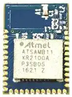
**Figure 1-1. Marking information**
**Datasheet Preliminary**
DS70005342A-page 6
© 2017 Microchip Technology Inc.
**ATSAMB11XR/ZR**
**2. Package Information**
**Table 2-1. ATSAMB11-XR2100A SiP 40 Package Information**
|**Parameter**|**Value**|**Units**|**Tolerance**|
|---|---|---|---|
|Package size|5.5 x 4.5|mm|±0.05 mm|
|Pad count|40|||
|Total thickness|1.36|mm|±0.05 mm|
|Pad pitch|0.4|||
|Pad width|0.21|||
|Exposed pad size|0.5 x 0.5|||
**Note:** For drawing details, see Figure 11-1.
**Table 2-2. ATSAMB11-ZR210CA Module Information**
|**Parameter**|**Value**|**Units**|**Tolerance**|
|---|---|---|---|
|Package size|7.503 x 10.541|mm|Untoleranced dimension|
|Pad count|34|||
|Total thickness|1.868|mm|Untoleranced dimensions|
|Pad pitch|0.61|||
|Pad width|0.406|||
|Exposed pad size|2.705 x 2.705|||
**Note:** For drawing details, see Figure 11-2.
**Datasheet Preliminary**
DS70005342A-page 7
© 2017 Microchip Technology Inc.
**ATSAMB11XR/ZR**
## **3. Block Diagram**
## **Figure 3-1. Block Diagram**
**Datasheet Preliminary**
DS70005342A-page 8
© 2017 Microchip Technology Inc.
**ATSAMB11XR/ZR**
## **4. Pinout Information**
The ATSAMB11-XR2100A is offered in an exposed pad 40-pin SiP package. This package has an exposed paddle that must be connected to the system board ground. The SiP package pin assignment is shown in the figure below. The color shading is used to indicate the pin type as follows:
- Red – analog
- Green – digital I/O (switchable power domain)
- Blue – digital I/O (always-on power domain)
- Yellow – power
- Purple – PMU
- Shaded green/red – configurable mixed-signal GPIO (digital/analog)
The ATSAMB11-ZR210CA module is a castellated PCB with the ATSAMB11-XR2100A integrated with a matched chip antenna. The pins are identified in the pin description table. The ATSAMB11-XR2100A also contains a paddle pad on the bottom of the PCB, that must be soldered to the system ground.
**Figure 4-1. ATSAMB11-XR2100A Pin Assignment**
**Datasheet Preliminary**
DS70005342A-page 9
© 2017 Microchip Technology Inc.
**ATSAMB11XR/ZR**
**Figure 4-2. ATSAMB11-ZR210CA Pin Descriptions**
The following table lists the pin assignments for both the ATSAMB11-XR2100A and the ATSAMB11ZR210CA.
**Table 4-1. ATSAMB11-XR2100A and ATSAMB11-ZR210CA Pin Description**
|**ATSAMB11-**<br>**XR2100A**<br>**Pin #**|**ATSAMB11-**<br>**ZR210CA**<br>**Pin #**|**Pin Name**|**Pin Type**|**Description / Default**<br>**Function**|
|---|---|---|---|---|
|1|-|LP_GPIO_23|Digital I/O|GPIO with Programmable Pull-<br>Up/Down|
|2|17|LP_GPIO_5|Digital I/O|GPIO with Programmable Pull-<br>Up/Down|
|3|18|LP_GPIO_6|Digital I/O|GPIO with Programmable Pull-<br>Up/Down|
|4|19|LP_GPIO_7|Digital I/O|GPIO with Programmable Pull-<br>Up/Down|
|5|20|LP_GPIO_8**(1)**|Digital I/O|GPIO with Programmable Pull-<br>Up/Down|
**Datasheet Preliminary**
DS70005342A-page 10
© 2017 Microchip Technology Inc.
**ATSAMB11XR/ZR**
|**ATSAMB11-**<br>**XR2100A**<br>**Pin #**|**ATSAMB11-**<br>**ZR210CA**<br>**Pin #**|**Pin Name**|**Pin Type**|**Description / Default**<br>**Function**|
|---|---|---|---|---|
|6|21|LP_GPIO_9**(1)**|Digital I/O|GPIO with Programmable Pull-<br>Up/Down|
|7|22|LP_GPIO_10|Digital I/O|GPIO with Programmable Pull-<br>Up/Down|
|8|23|LP_GPIO_11|Digital I/O|GPIO with Programmable Pull-<br>Up/Down|
|9|24|LP_GPIO_12|Digital I/O|GPIO with Programmable Pull-<br>Up/Down|
|10|25|LP_GPIO_13|Digital I/O|GPIO with Programmable Pull-<br>Up/Down|
|11|27|VBAT|Power supply|Power supply pin for the<br>DC/DC convertor|
|12|28|GPIO_MS1|Mixed Signal I/O|GPIO with Programmable Pull-<br>Up/Down|
|13|29|GPIO_MS2|Mixed Signal I/O|GPIO with Programmable Pull-<br>Up/Down|
|14|30|C_EN|Digital Input|Can be used to control the<br>state of PMU. High level<br>enables the module; low- level<br>places module in Power- Down<br>mode.|
|15|31|GPIO_MS3|Mixed Signal I/O|GPIO with Programmable Pull-<br>Up/Down|
|16|32|GPIO_MS4|Mixed Signal I/O|GPIO with Programmable Pull-<br>Up/Down|
|17|33|RTC_CLK_P|Analog|Crystal pin or External clock<br>supply, see32.768 kHz RTC<br>Crystal Oscillator (RTC XO)|
|18|34|RTC_CLK_N|Analog|Crystal pin or External clock<br>supply, see32.768 kHz RTC<br>Crystal Oscillator (RTC XO)|
|19|-|AO_TM|Digital Input|Always On Test Mode. Connect<br>to GND|
|20|1|AO_GPIO_0|Always On Digital<br>I/O, Programmable<br>Pull-Up|To be held in logic '0' GND to<br>allow the device to enter<br>Ultra_Low_Power mode|
**Datasheet Preliminary**
DS70005342A-page 11
© 2017 Microchip Technology Inc.
**ATSAMB11XR/ZR**
|**ATSAMB11-**<br>**XR2100A**<br>**Pin #**|**ATSAMB11-**<br>**ZR210CA**<br>**Pin #**|**Pin Name**|**Pin Type**|**Description / Default**<br>**Function**|
|---|---|---|---|---|
|||||Can be used to Wakeup the<br>device from Ultra_Low_Power<br>mode.|
|21|2|AO_GPIO_1|Always On. Digital<br>I/O, Programmable<br>Pull- Up|GPIO with Programmable Pull-<br>Up|
|22|3|AO_GPIO_2|Always On. Digital<br>I/O, Programmable<br>Pull- Up|GPIO with Programmable Pull-<br>Up|
|23|4|LP_GPIO_14|Digital I/O|GPIO with Programmable Pull-<br>Up/Down|
|24|5|LP_GPIO_15|Digital I/O|GPIO with Programmable Pull-<br>Up/Down|
|25|-|LP_GPIO_24|Digital I/O|GPIO with Programmable Pull-<br>Up/Down|
|26|6|LP_GPIO_16|Digital I/O|GPIO with Programmable Pull-<br>Up/Down|
|27|7|VDDIO|Power supply|Power supply pin for the I/O<br>pins. Can be less than or equal<br>to voltage supplied at VBAT|
|28|8|LP_GPIO_17|Digital I/O|GPIO with Programmable Pull-<br>Up/Down|
|29|9|LP_GPIO_18|Digital I/O|GPIO with Programmable Pull-<br>Up/Down|
|30|10|LP_GPIO_19|Digital I/O|GPIO with Programmable Pull-<br>Up/Down|
|31|-|TPP||Do not connect|
|32|11, 26|GND|Ground||
|33|-|RFIO|Analog I/O|RX input and TX output. Single-<br>ended RF I/O; To be connected<br>to antenna|
|34|-|NC||Do not connect|
|35|12|LP_GPIO_0|Digital I/O|SWD clock|
|36|13|LP_GPIO_1|Digital I/O|SWD I/O|
|37|14|LP_GPIO_2|Digital I/O|GPIO with Programmable Pull-<br>Up/Down|
**Datasheet Preliminary**
DS70005342A-page 12
© 2017 Microchip Technology Inc.
**ATSAMB11XR/ZR**
|**ATSAMB11-**<br>**XR2100A**<br>**Pin #**|**ATSAMB11-**<br>**ZR210CA**<br>**Pin #**|**Pin Name**|**Pin Type**|**Description / Default**<br>**Function**|
|---|---|---|---|---|
|38|15|LP_GPIO_3|Digital I/O|GPIO with Programmable Pull-<br>Up/Down|
|39|16|LP_GPIO_4|Digital I/O|GPIO with Programmable Pull-<br>Up/Down|
|40|-|LP_GPIO_22|Digital I/O|GPIO with Programmable Pull-<br>Up/Down|
|41|35|Paddle|Ground|Exposed paddle must be<br>soldered to system ground|
## **Note:**
1. These GPIO pads are high-drive pads. Refer Table 10-3.
**Datasheet Preliminary**
DS70005342A-page 13
© 2017 Microchip Technology Inc.
**ATSAMB11XR/ZR**
## **5. Device States**
This section includes details on the description and controlling of the Device states.
## **5.1 Description of Device States**
The ATSAMB11-XR2100A and the ATSAMB11-ZR210CA have multiple device states, depending on the state of the ARM processor and BLE subsystem.
**Note:** The ARM is required to be powered on, if the BLE subsystem is active.
- BLE_On_Transmit – Device is actively transmitting a BLE signal.
- BLE_On_Receive – Device is in active receive state.
- MCU_Only – Device has ARM processor powered-on and BLE subsystem powered-down.
- Ultra_Low_Power – BLE subsystem and ARM processor are powered-down.
- Power_Down – Device core supply off.
## **5.1.1**
## **Controlling the Device States**
The following pins are used to switch between the main device states:
- C_EN – used to enable PMU
- VDDIO – I/O supply voltage from an external power supply
- AO_GPIO_0 - can be used to control the device from entering/exiting Ultra_Low_Power mode
To be in the Power_Down state, the VDDIO supply must be turned on and the C_EN must be maintained at logic low (at GND level). To switch between the Power_Down state and the MCU_Only state, C_EN must be maintained at logic high (VDDIO voltage level). Once the device is in the MCU_Only state, all other state transitions are controlled entirely by software. When VDDIO supply is turned off and C_EN is in logic low, the chip is powered off with no leakage.
When VDDIO supply is turned off, voltage cannot be applied to the ATSAMB11-XR2100A pins, as each pin contains an ESD diode from the pin to supply. This diode turns on, when a voltage higher than one diode-drop is supplied to the pin.
If voltage is applied to the signal pads while the chip is in a low power state, the VDDIO supply must be on so the Power_Down state is used. Similarly, to prevent the pin-to-ground diode from turning on, do not apply a voltage that is more than one diode-drop below ground to any pin.
The AO_GPIO_0 pin can be used to control the device from entering and exiting Ultra_Low_Power mode. When AO_GPIO_0 is maintained in logic high state, the device will not enter Ultra_Low_Power mode. When the AO_GPIO_0 is maintained in logic low, the device will enter Ultra_Low_Power mode provided there are no BLE events to be handled. To achieve the lowest power consumption in Ultra_Low_Power mode, AO_GPIO_0 pin must be held in logic low.
## **5.2 Power Sequences**
The power sequences and timing parameters for the ATSAMB11-XR2100A and ATSAMB11-ZR210CA, are illustrated below.
**Datasheet Preliminary**
DS70005342A-page 14
© 2017 Microchip Technology Inc.
**ATSAMB11XR/ZR**
**Figure 5-1. Power-up/Power-down Sequence**
The timing parameters are provided in following table.
**Table 5-1. Power-up/Power-down Sequence Timing**
|**Parameter **<br>~~a~~|**Min. **<br>~~a~~|**Max. **<br>~~a~~|**Units**<br>~~a~~|**Description**|**Notes**<br>~~eee~~|
|---|---|---|---|---|---|
|tA<br>~~a~~|0<br>~~a~~|~~a~~|ms<br>~~a~~|VBAT rise to VDDIO rise|VBAT and VDDIO can rise<br>simultaneously or can be tied together<br>~~eee~~|
|tB|0|||VDDIO rise to C_EN rise|C_EN must not rise before VDDIO. C_EN<br>must be driven high or low, not left<br>floating.|
|tC|10||µs|C_EN rise to 31.25 kHz (2<br>MHz/64) oscillator stabilizing||
|tB'|0||ms|C_EN fall to VDDIO fall|C_EN must fall before VDDIO. C_EN<br>must be driven high or low, not left<br>floating.|
|tA'|0|||VDDIO fall to VBAT fall|VBAT and VDDIO can fall simultaneously<br>or be tied together|
## **5.3 Digital and Mixed-Signal I/O Pin Behavior during Power-Up Sequences**
The following table represents I/O pin states corresponding to device power modes.
**Datasheet Preliminary**
DS70005342A-page 15
© 2017 Microchip Technology Inc.
**ATSAMB11XR/ZR**
## **Table 5-2. I/O Pin Behavior in the Different Device States[(1)]**
|**Device State**|**VDDIO **|**CHIP_EN**|**Output Driver**|**Input Driver**|**Pull Up/Down**<br>**Resistor(2)**|
|---|---|---|---|---|---|
|Power_Down: core supply<br>off|High|Low|Disabled (Hi-Z)|Disabled|Disabled|
|Power-on Reset: core<br>supply on, POR hard reset<br>pulse on|High|High|Disabled (Hi-Z)|Disabled|Disabled**(3)**|
|Power-on Default: core<br>supply on, device out of<br>reset but not programmed<br>yet|High|High|Disabled (Hi-Z)|Enabled**(4)**|Enabled Pull-Up**(4)**|
|MCU_Only, BLE_On: core<br>supply on, device<br>programmed by firmware|High|High|Programmed by<br>firmware for each<br>pin: Enabled or<br>Disabled (Hi-Z)<br>**(5)**,when Enabled<br>driving 0 or 1|Opposite of<br>Output<br>Driver state:<br>Disabled or<br>Enabled**(5)**|Programmed by<br>firmware for each<br>pin: Enabled or<br>Disabled, Pull-Up<br>or Pull- Down**(5)**|
|Ultra_Low_Power:<br>core supply on for always-<br>on domain, core supply off<br>for switchable domains|High|High|Retains previous<br>state**(6)**for each pin:<br>Enabled or Disabled<br>(Hi-Z), when<br>Enabled driving 0 or<br>1|Opposite of<br>Output<br>Driver state:<br>Disabled or<br>Enabled**(6)**|Retains previous<br>state**(6)**for each<br>pin: Enabled or<br>Disabled, Pull-Up<br>or Pull-Down|
## **Note:**
1. This table applies to all three types of I/O pins (digital switchable domain GPIOs, digital always-on/ wake-up GPIO, and mixed-signal GPIOs) unless otherwise noted.
2. Pull-up/down resistor value is 96 kOhm ±10%.
3. In Power-on Reset state, the pull-up resistor is enabled in the always-on/wake-up GPIO only.
4. In Power-on Default state, the input drivers and pull-up/down resistors are disabled in the mixedsignal GPIOs only (mixed-signal GPIOs are defaulted to analog mode, see the note below).
5. Mixed-signal GPIOs can be programmed to be in analog or digital mode for each pin: when programmed to analog mode (default), the output driver, input driver, and pull-up/down resistors are all disabled.
6. In Ultra_Low_Power state, the always-on/wake-up GPIO does not have retention capability and behaves same as in MCU_Only or BLE_On states, also for mixed-signal GPIOs programming analog mode overrides retention functionality for each pin.
**Datasheet Preliminary**
DS70005342A-page 16
© 2017 Microchip Technology Inc.
**ATSAMB11XR/ZR**
## **6. Clocking**
## **6.1 Overview**
**Figure 6-1. Clock Architecture**
Figure 6-1 provides an overview of the clock tree and clock management blocks.
The BLE Clock is used to drive the BLE subsystem. The ARM clock is used to drive the Cortex-M0 MCU and its interfaces (UART, SPI, and I[2] C); the recommended MCU clock speed is 26 MHz. The Low Power Clock is used to drive all the low-power applications like the BLE sleep timer, always-on power sequencer, always-on timer, and others.
The 26 MHz integrated RC Oscillator is used for most general purpose operations on the MCU and its peripherals. In cases when the BLE subsystem is not used, the RC oscillator can be used for lower power consumption. The frequency variation of this RC oscillator is up to ±50% over process, voltage, and temperature.
The frequency variation of 2 MHz integrated RC Oscillator is up to ±50% over process, voltage, and temperature.
The 32.768 kHz RTC Crystal Oscillator (RTC XO) is used for BLE operations as it will reduce power consumption by providing the best timing for wake-up precision, allowing circuits to be in low-power sleep mode for as long as possible until they need to wake-up and connect during the BLE connection event.
## **6.2 26 MHz Crystal Oscillator (XO)**
A 26 MHz crystal oscillator is integrated into the ATSAMB11-XR2100A and ATSAMB11-ZR210CA to provide the precision clock for the BLE operations.
**Datasheet Preliminary**
DS70005342A-page 17
© 2017 Microchip Technology Inc.
**ATSAMB11XR/ZR**
## **6.3 32.768 kHz RTC Crystal Oscillator (RTC XO)**
## **6.3.1 General Information**
The ATSAMB11-XR2100A and ATSAMB11-ZR210CA contain a 32.768 kHz RTC oscillator that is preferably used for BLE activities involving connection events. To be compliant with the BLE specifications for connection events, the frequency accuracy of this clock has to be within ±500 ppm. Because of the high accuracy of the 32.768 kHz crystal oscillator clock, the power consumption can be minimized by leaving radio circuits in low-power sleep mode for as long as possible, until they need to wake-up for the next connection timed event.
The block diagram in Figure 6-2 below shows how the internal low-frequency Crystal Oscillator (XO) is connected to the external crystal.
The RTC XO has a programmable internal capacitance with a maximum of 15 pF on each terminal, RTC_CLK_P, and RTC_CLK_N. When bypassing the crystal oscillator with an external signal, the user can program down the internal capacitance to its minimum value (~1 pF) for easier driving capability. The driving signal can be applied to the RTC_CLK_P terminal, as illustrated in Figure 6-2 below.
The need for external bypass capacitors depends on the chosen crystal characteristics. Typically, the crystal should be chosen to have a load capacitance of 7 pF to minimize the oscillator current. Refer to the datasheet of the preferred crystal and take into account the on-chip capacitance.
Alternatively, if an external 32.768 kHz clock is available, it can be used to drive the RTC_CLK_P pin instead of using a crystal. The XO has 6 pF internal capacitance on the RTC_CLK_P pin. To bypass the crystal oscillator, an external signal capable of driving 6 pF can be applied to the RTC_CLK_P terminal, as illustrated in Figure 6-2. RTC_CLK_N must be left unconnected, when driving an external source into RTC_CLK_P. Refer to the Table 6-1 for the specification of the external clock to be supplied at RTC_CLK_P.
**Figure 6-2. Connections to RTC XO**
**Datasheet Preliminary**
DS70005342A-page 18
© 2017 Microchip Technology Inc.
**ATSAMB11XR/ZR**
**Table 6-1. 32.768 kHz External Clock Specification**
|**Parameter**|**Min.**|**Typ.**|**Max**|**Unit**|**Comments**|
|---|---|---|---|---|---|
|Oscillation frequency||32.768||kHz|Must be able to drive 6 pF load at desired frequency|
|VinH|0.7||1.2|V|High level input voltage|
|VinL|0||0.2||Low level input voltage|
|Stability – Temperature|-250||+250|ppm||
Additional internal trimming capacitors (C_onchip) are available. They provide the possibility to tune the frequency output of RTC XO without changing the external load capacitors. Contact technical support for usage of the internal trimming capacitors.
## **Note:**
Refer the BluSDK BLE API Software Development Guide for details on how to enable the 32.768 kHz clock output and tune the internal trimming capacitors.
**Table 6-2. 32.768 kHz XTAL C_onchip Programming**
|**Register: pierce_cap_ctrl[3:0]**|**C_onchip [pF]**|
|---|---|
|0000|0.0|
|0001|1.0|
|0010|2.0|
|0011|3.0|
|0100|4.0|
|0101|5.0|
|0110|6.0|
|0111|7.0|
|1000|8.0|
|1001|9.0|
|1010|10.0|
|1011|11.0|
|1100|12.0|
|1101|13.0|
|1110|14.0|
|1111|15.0|
## **6.3.2 RTC XO Design and Interface Specification**
The RTC consists of two main blocks: The Programmable Gm stage and tuning capacitors. The programmable Gm stage is used to guarantee start-up and to sustain oscillation. Tuning capacitors are used to adjust the XO center frequency and control the XO precision for different crystal models. The output of the XO is driven to the digital domain via a digital buffer stage with a supply voltage of 1.2V.
**Datasheet Preliminary**
DS70005342A-page 19
© 2017 Microchip Technology Inc.
**ATSAMB11XR/ZR**
**Table 6-3. RTC XO Interface**
|**Pin Name**|**Function**|**Register Default**|
|---|---|---|
|Digital Control Pins|||
|Pierce_res_ctrl|Control feedback resistance value:<br>0 = 20 MOhm Feedback resistance<br>1 = 30 MOhm Feedback resistance|0X4000F404<15>=’1’|
|Pierce_cap_ctrl<3:0>|Control the internal tuning capacitors with step of<br>700 fF:<br>0000=700 fF<br>1111=11.2 pF<br>Refer to crystal datasheet to check for optimum<br>tuning cap value|0X4000F404<23:20>=”1000”|
|Pierce_gm_ctrl<3:0>|Controls the Gm stage gain for different crystal<br>mode:<br>0011= for crystal with shunt capacitance of 1.2 pF<br>1000= for crystal with shunt capacitance of >3 pF|0X4000F404<19:16>=”1000”|
|VDD_XO|1.2V||
## **6.3.3 RTC Characterization with Gm Code Variation at Supply 1.2V and Temp. = 25°C**
This section shows the RTC total drawn current and the XO accuracy versus different tuning capacitors and different GM codes, at a supply voltage of 1.2V and temperature = 25°C.
## **Figure 6-3. RTC Drawn Current vs. Tuning Caps at 25°C**
**Datasheet Preliminary**
DS70005342A-page 20
© 2017 Microchip Technology Inc.
**ATSAMB11XR/ZR**
**Figure 6-4. RTC Oscillation Frequency Deviation vs. Tuning Caps at 25°C**
## **6.3.4 RTC Characterization with Supply Variation and Temp. = 25°C Figure 6-5. RTC Drawn Current vs. Supply Variation**
**Datasheet Preliminary**
DS70005342A-page 21
© 2017 Microchip Technology Inc.
**ATSAMB11XR/ZR**
**Figure 6-6. RTC Frequency Deviation vs. Supply Voltage**
## **6.4 2 MHz Integrated RC Oscillator**
The 2 MHz integrated RC Oscillator circuit without calibration contains a frequency variation of 50% over process, temperature, and voltage variation. As described above, calibration over process, temperature, and voltage is required to maintain the accuracy of this clock.
**Figure 6-7. 32 kHz RC Oscillator PPM Variation vs. Calibration Time at Room Temperature**
**Datasheet Preliminary**
DS70005342A-page 22
© 2017 Microchip Technology Inc.
**ATSAMB11XR/ZR**
## **Figure 6-8. 32 kHz RC Oscillator Frequency Variation over Temperature**
**Datasheet Preliminary**
DS70005342A-page 23
© 2017 Microchip Technology Inc.
**ATSAMB11XR/ZR**
## **7. CPU and Memory Subsystem**
## **7.1 ARM Subsystem**
The ATSAMB11-XR2100A and ATSAMB11-ZR210CA have an ARM Cortex-M0 32-bit processor. It is responsible for controlling the BLE Subsystem and handling all application features.
The Cortex-M0 Microcontroller consists of a full 32-bit processor capable of addressing 4GB of memory. It has a RISC like load/store instruction set and internal 3-stage Pipeline Von Neumann architecture.
The Cortex-M0 processor provides a single system-level interface using AMBA technology to provide high speed, low latency memory accesses.
The Cortex-M0 processor implements a complete hardware debug solution with four hardware breakpoint and two watchpoint options. This provides high system visibility of the processor, memory, and peripherals through a 2-pin Serial Wire Debug (SWD) port that is ideal for microcontrollers and other small package devices.
ATSAMB11 is running a proprietary RTOS tightly coupled with FW in the ROM and the user can not override it. SysTick timer is being used by the stack and will not be available for usage by the application.
**Figure 7-1. ARM Cortex-M0 Subsystem**
**Datasheet Preliminary**
DS70005342A-page 24
© 2017 Microchip Technology Inc.
**ATSAMB11XR/ZR**
## **7.1.1 Features**
The processor features and benefits are:
- Tight integration with the system peripherals to reduce area and development costs
- Thumb instruction set combines high code density with 32-bit performance
- Integrated sleep modes using a Wakeup Interrupt Controller for low power consumption
- Deterministic and high-performance interrupt handling via Nested Vector Interrupt Controller for time-critical applications
- Serial Wire Debug reduces the number of pins required for debugging
- DMA engine for Peripheral-to-Memory, Memory-to-Memory, and Memory-to-Peripheral operation
## **7.1.2**
## **Wakeup Sources**
Ultra_Low_Power is the lowest possible power state for the system. In Ultra_Low_Power state, ARM Cortex-M0, BLE core, GPIO's, and all other peripheral cores are powered-down. Only AON-GPIO_0 and AON-Sleep timer are functional in this state.
ATSAMB11 contains the following wake-up sources that wake up the system from Ultra_Low_Power mode:
- BLE events
- AON-GPIO_0
- AON-Sleep timer
## **7.1.3 ARM Module Descriptions**
## **7.1.3.1**
## **Timer**
The 32-bit timer block allows the CPU to generate a time tick at a programmed interval. This feature can be used for a wide variety of functions such as counting, interrupt generation, and time tracking.
**Note:** ARM Timer is one of the reserved resources being used by the BLE stack. Application must refrain from using this peripheral.
## **7.1.3.2 Dual Timer**
The APB dual-input timer module is an APB slave module consisting of two programmable 32-bit downcounters that can generate interrupts when they expire. The timer can be used in a Free-running, Periodic, or One-shot mode.
## **7.1.3.3**
## **Watchdog Timer**
The two watchdog blocks allow the CPU to be interrupted, if it has not interacted with the watchdog timer before it expires. In addition, this interrupt will be an output of the core, so that it can be used to reset the CPU in the event that a direct interrupt to the CPU is not useful. This will allow the CPU to get back to a known state in the event, a program is no longer executing as expected. The watchdog module applies a reset to a system in the event of a software failure, providing a way to recover from software crashes.
Watchdog timer 0 is a reserved resource, being used by the BLE stack. Application must refrain from using the watchdog timer 0.
## **7.1.3.4 Always-On (AON) sleep Timer**
This timer is a 32-bit countdown timer that operates on the 32 kHz sleep clock. It can be used as a general-purpose timer for the ARM or as a wake-up source for the chip. It has the ability to be a one-time programmable timer, as it will generate an interrupt/wake-up on expiration and stop operation. It also has the ability to be programmed in an auto reload fashion, where it will generate an interrupt/wake-up and then proceed to start another countdown sequence.
**Datasheet Preliminary**
DS70005342A-page 25
© 2017 Microchip Technology Inc.
**ATSAMB11XR/ZR**
- **7.1.3.5 SPI Controller**
See Section SPI Master/Slave Interface.
## **7.1.3.6 I[2] C Controller**
See Section I2C Master/Slave Interface.
- **7.1.3.7 SPI-Flash Controller**
The AHB SPI-Flash Controller is used to access the internal stacked SPI Flash to access various instruction/data code required for storing application code, code patches, and OTA images. It supports several SPI modes including 0, 1, 2, and 3. See Section SPI Flash Master Interface.
- **7.1.3.8 UART**
See Section UART Interface.
- **7.1.3.9 DMA Controller**
Direct Memory Access (DMA) allows certain hardware subsystems to access main system memory independent of the Cortex-M0 Processor.
The DMA features and benefits are:
- Supports any address alignment
- Supports any buffer size alignment
- Peripheral flow control and peripheral block transfer
- The following modes are supported:
- Peripheral to peripheral transfer
- Memory to memory
- Memory to peripheral
- Peripheral to memory
- Register to memory
- Interrupts for both TX done and RX done in memory and peripheral mode
- Scheduled transfers
- Endianness byte swapping
- Watchdog timer
- 4-channel operation
- 32-bit Data width
- AHB MUX (on read and write buses)
- Command lists support
- Usage of tokens
## **7.1.3.10 Nested Vector Interrupt Controller**
External interrupt signals connect to the NVIC, and the NVIC prioritizes the interrupts. Software can set the priority of each interrupt. The NVIC and the Cortex-M0 processor core are closely coupled to provide low-latency interrupt processing and efficient processing of late arriving interrupts.
All NVIC registers are accessible via word transfers and are little endian. Any attempt to read or write a half-word or byte individually is unpredictable.
The NVIC allows the CPU to be able to individually enable or disable each interrupt source, and hold each interrupt until it is serviced and cleared by the CPU.
**Datasheet Preliminary**
DS70005342A-page 26
© 2017 Microchip Technology Inc.
**ATSAMB11XR/ZR**
**Table 7-1. NVIC Register Summary**
|**Name**|**Description**|
|---|---|
|ISER|Interrupt Set-Enable Register|
|ICER|Interrupt Clear-Enable Register|
|ISPR|Interrupt Set-Pending Register|
|ICPR|Interrupt Clear-Pending Register|
|IPR0-IPR7|Interrupt Priority Registers|
**Note:** For a description of each register, see the Cortex-M0 documentation from ARM.
The Cortex-M0 NVIC is connected to 32 IRQ sources. Some of the interrupt sources are marked reserved for internal operation of the BLE functionality and ROM code of the ATSAMB11.
The following table lists the interrupts that are available in ATSAMB11. Also, some of the interrupts are marked as RESERVED as they are used by the BLE stack and are used for firmware in general. Applications must refrain from registering an ISR for those interrupts as it affects the chip functionality.
**Table 7-2. ATSAMB11 Interrupts**
|**ISR index**|**Interrupt Source**|**Availability**|
|---|---|---|
|0|UART0 RX|Available/Muxable|
|1|UART0 TX|Available/Muxable|
|2|UART1 RX|Available/Muxable|
|3|UART1 TX|Available/Muxable|
|4|SPI0 RX|Available/Muxable|
|5|SPI0 TX|Available/Muxable|
|6|SPI1 RX|Available/Muxable|
|7|SPI1 TX|Available/Muxable|
|8|I2C0 RX|Available/Muxable|
|9|I2C0 TX|Available/Muxable|
|10|I2C1 RX|Available/Muxable|
|11|I2C1 TX|Available/Muxable|
|12|Watchdog 0|RESERVED|
|13|Watchdog 1|Available/Muxable|
|14|ARM<br>®Dual Timer|Available/Muxable|
|15|BLE specific|RESERVED|
|16|RESERVED|Available/Muxable|
|17|BLE specific|RESERVED|
|18|SPI Flash|Available/Muxable|
**Datasheet Preliminary**
DS70005342A-page 27
© 2017 Microchip Technology Inc.
**ATSAMB11XR/ZR**
|19|BLE specific|RESERVED|
|---|---|---|
|20|Brown Out Detected|Available/Muxable|
|21|BLE specific|RESERVED|
|22|BLE specific|RESERVED|
|23|GPIO 0 Combined|Available/Non-Muxable|
|24|GPIO 1 Combined|Available/Non-Muxable|
|25|GPIO 2 combined|Available/Non-Muxable|
|26|ARM timer|RESERVED|
|27|AON sleep timer|Available/Non-Muxable|
|28|BLE specific|RESERVED|
|29|BLE specific|RESERVED|
|30|BLE specific|RESERVED|
|31|BLE specific|RESERVED|
The following table provides the list of interrupt options available for each of the muxable interrupt.
**Table 7-3. ATSAMB11 Muxable Interrupt options**
|**Option**|**Interrupt Source**|
|---|---|
|0x1|UART0 RX|
|0x2|UART0 TX|
|0x3|UART1 RX|
|0x4|UART1 TX|
|0x5|SPI0 RX|
|0x6|SPI0 TX|
|0x7|SPI1 RX|
|0x8|SPI1 TX|
|0x9|I2C0 RX|
|0xA|I2C0 TX|
|0xB|I2C1 RX|
|0xC|I2C1 TX|
|0xD|WDT0 – RESERVED|
|0xE|WDT1|
|0xF|ARM DUALTIMER|
|0x10|DMA STATUS|
|0x11|SECURITY|
**Datasheet Preliminary**
DS70005342A-page 28
© 2017 Microchip Technology Inc.
**ATSAMB11XR/ZR**
|0x12|RESERVED|
|---|---|
|0x13|QUAD DECODER|
|0x14|RESERVED|
|0x15|RESERVED|
|0x16|RESERVED|
|0x17|RESERVED|
|0x18|BROWNOUT DETECTED|
## **7.1.3.11 GPIO Controller**
The AHB GPIO is a general-purpose I/O interface unit that allows the CPU to independently control all input or output signals on the ATSAMB11-XR2100A and ATSAMB11-ZR210CA. These can be used for a wide variety of functions pertaining to the application.
The AHB GPIO provides a 16-bit I/O interface with the following features:
- Programmable interrupt generation capability
- Programmable masking support
- Thread-safe operation by providing separate set and clear addresses for control registers
- Inputs are sampled using a double flip-flop to avoid meta-stability issues
## **7.2 Memory Subsystem**
The Cortex-M0 core uses a 128 KB instruction/boot ROM along with a 128 KB shared instruction and data RAM.
Refer to BluSDK SMART BLE API Software Development Guide for the memory map of this memory section.
## **7.2.1**
## **Shared Instruction and Data Memory**
The Instruction and Data Memory (IDRAM1 and IDRAM2) contains instructions and data used by the ARM. The 128 KB size of IDRAM1 and IDRAM2 is used for BLE subsystem and also for the user application. IDRAM1 contains three 32 KB memories and IDRAM2 contains two 16 KB memories that are accessible to the ARM and used for instruction/data storage.
## **7.2.2 ROM**
The ROM is used to store the boot code and BLE firmware, stack, and selected user profiles. The ROM contains the 128 KB memory that is accessible to the ARM. The Boot loader code stored in ROM loads the application from Flash to RAM.
## **7.2.3**
## **BLE Retention Memory**
The BLE functionality requires 8 KB state, instruction, and data to be retained in memory, when the processor either goes into Sleep mode or Power down mode. The RAM is separated into specific power domains to allow tradeoff in power consumption with retention memory size.
## **7.3 Non-Volatile Memory**
The ATSAMB11-XR2100A and ATSAMB11-ZR210CA have 768 bits of non-volatile eFuse memory that can be read by the CPU after device reset. This memory region is one-time- programmable. It is
**Datasheet Preliminary**
DS70005342A-page 29
© 2017 Microchip Technology Inc.
**ATSAMB11XR/ZR**
partitioned into six 128-bit banks. Each bank is divided into four blocks with each block containing 32 bits of memory locations. This non-volatile, one-time-programmable memory is used to store customer specific parameters as listed below.
- 26 MHz XO Calibration information
- BT address
The bit map for the block containing the above parameters is detailed in the following figures.
**Figure 7-2. Bank 5 Block 0**
**Figure 7-3. Bank 5 Block 1**
**Datasheet Preliminary**
DS70005342A-page 30
© 2017 Microchip Technology Inc.
**ATSAMB11XR/ZR**
**Figure 7-4. Bank 5 Block 3**
The bits that are not depicted in the above register description are all reserved for future use.
## **7.3.1 26 MHz XO Calibration information**
Information for both ATSAMB11-XR2100A and ATSAMB11-ZR210CA will be pre-programmed.
## **7.3.2**
## **BT Address**
These bits contain the BT address used by the user application. For ATSAMB11-ZR210CA modules, the BT address is pre-programmed. For ATSAMB11-XR2100A, the user must purchase the MAC address from IEEE and program it to the designated bit locations of the non-volatile memory.
## **7.3.3**
## **Flash Memory**
The ATSAMB11-XR2100A and ATSAMB11-ZR210CA have 256 kB of Flash memory, stacked on top of the MCU and BLE SoC. It is accessed through the SPI Flash controller.
Flash memory features are:
- 256 bytes per programmable page
- Uniform 4 kB Sectors, 32 kB & 64 kB Blocks
- Sector Erase (4 Kbyte)
- Block Erase (32K or 64 Kbyte)
- Page program up to 256 bytes <1 ms
- More than 100,000 erase/write cycles and more than 20-year data retention
- 2.3V to 3.6V supply range
Refer to BluSDK SMART BLE API Software Development Guide for the memory map of this memory section.
**Datasheet Preliminary**
DS70005342A-page 31
© 2017 Microchip Technology Inc.
**ATSAMB11XR/ZR**
## **8. Bluetooth Low Energy (BLE) Subsystem**
The BLE subsystem implements all the critical real-time functions required for full compliance with specification of the Bluetooth System, v4.1, Bluetooth SIG.
It consists of a Bluetooth 4.1 baseband controller (core), radio transceiver and the Microchip Bluetooth Smart Stack, the BLE Software Platform.
## **8.1 BLE Core**
The baseband controller consists of a modem and a Medium Access Controller (MAC) through which it encodes and decodes HCI packets. In addition, it constructs baseband data packages and schedules frames, and manages and monitors connection status, slot usage, data flow, routing, segmentation and buffer control.
The core performs Link Control Layer management supporting the main BLE states, including advertising and connection.
## **8.2 Features**
- Broadcaster, Central, Observer, Peripheral
- Simultaneous Master and Slave operation, connect up to eight connections
- Frequency Hopping
- Advertising/Data/Control packet types
- Encryption (AES-128, SHA-256)
- Bitstream processing (CRC, whitening)
- Operating clock 52 MHz
## **8.3 BLE Radio**
The radio consists of a fully integrated transceiver, Low Noise Amplifier, Receive (RX) down converter, analog baseband processing, Phase Locked Loop (PLL), Transmit (TX) Power Amplifier, and Transmit/ Receive switch. At the RF front end, no external RF components on the PCB are required other than the antenna and a matching component.
**Table 8-1. ATSAMB11 BLE Radio features and properties**
|**Feature**|**Description**|
|---|---|
|Part Number|ATSAMB11-XR2100A and ATSAMB11-ZR210CA|
|BLE Standard|Bluetooth V4.1 – Bluetooth Low Energy|
|Frequency range|2402 MHz to 2480 MHz|
|Number of channels|40|
|Modulation|GFSK|
|Data rate|1 Mbps|
**Datasheet Preliminary**
DS70005342A-page 32
© 2017 Microchip Technology Inc.
**ATSAMB11XR/ZR**
## **8.4**
## **Microchip BluSDK Smart**
The BluSDK Smart offers a comprehensive set of tools including reference applications for several Bluetooth SIG defined profiles and custom profile. This will help the user quickly evaluate, design and develop BLE products with ATSAMB11-XR2100A and ATSAMB11-ZR210CA.
The ATSAMB11-XR2100A and ATSAMB11-ZR210CA have a completely integrated Bluetooth Low Energy stack on chip that is fully qualified, mature, and Bluetooth V4.1 compliant.
Customer applications interface with the BLE protocol stack through the Microchip BLE API, which supports direct access to the GAP, SMP, ATT, GATT client / server, and L2CAP service layer protocols in the embedded firmware.
The stack includes numerous BLE profiles for applications like:
- Smart Energy
- Consumer Wellness
- Home Automation
- Security
- Proximity Detection
- Entertainment
- Sports and Fitness
- Automotive
Together with the Atmel Studio Software Development environment, the additional customer profiles can be easily developed.
The Bluetooth SmartConnect software development kit is based on Keil compiler tools and contains numerous application code examples for embedded mode. In addition to the protocol stack, the drivers for each peripheral hardware block are provided as part of the Atmel Software Framework (ASF).
## **8.4.1 Direct Test Mode (DTM) Example Application**
One among the reference application offered in BluSDK Smart is a DTM example application. Using this application, the user will be able to configure the device in the different test modes as defined in the Bluetooth Low Energy Core 4.1 specification (Vol6,Part F Direct Test Mode). Please refer the example getting started guide available in the BluSDK Smart release package.
**Datasheet Preliminary**
DS70005342A-page 33
© 2017 Microchip Technology Inc.
**ATSAMB11XR/ZR**
## **9. External Interfaces**
## **9.1 Overview**
The ATSAMB11-XR2100A and ATSAMB11-ZR210CA external interfaces include: 2xSPI Master/Slave (SPI0 and SPI1), 2xI[2] C Master/Slave (I[2] C0 and I[2] C1), 1xI[2] C Slave-only (I[2] C2), 2xUART (UART1 and UART2), 1xSPI Flash, 1xSWD, and General Purpose Input/Output (GPIO) pins.
Table 9-1 illustrates the different peripheral functions that are software selectable for each pin. This allows for maximum flexibility of mapping desired interfaces on GPIO pins. The MUX1 option allows for any MEGAMUX option from Table 9-2 to be assigned to a GPIO.
**Table 9-1. Pin-MUX Matrix of External Interfaces**
|**Pin Name**|**XR**<br>**Pin**<br>**#**|**ZR**<br>**Pin**<br>**#**|**Pull**|**MUX0**|**MUX1**|**MUX2**|**MUX3 **|**MUX4 **|**MUX5 **|**MUX6**|**MUX7**|
|---|---|---|---|---|---|---|---|---|---|---|---|
|LP_GPIO_0|35|12|Up/<br>Down|GPIO<br>0|MEGAMUX<br>0|SWD<br>CLK|||||TEST<br>OUT 0|
|LP_GPIO_1|36|13|Up/<br>Down|GPIO<br>1|MEGAMUX<br>1|SWD<br>I/O|||||TEST<br>OUT 1|
|LP_GPIO_2|37|14|Up/<br>Down|GPIO<br>2|MEGAMUX<br>2|UART1<br>RXD||SPI1<br>SCK|SPI0<br>SCK|SPI<br>FLASH<br>SCK|TEST<br>OUT 2|
|LP_GPIO_3|38|15|Up/<br>Down|GPIO<br>3|MEGAMUX<br>3|UART1<br>TXD||SPI1<br>MOSI|SPI0<br>MOSI|SPI<br>FLASH<br>TXD|TEST<br>OUT 3|
|LP_GPIO_4|39|16|Up/<br>Down|GPIO<br>4|MEGAMUX<br>4|UART1<br>CTS||SPI1<br>SSN|SPI0<br>SSN|SPI<br>FLASH<br>SSN|TEST<br>OUT 4|
|LP_GPIO_5|2|17|Up/<br>Down|GPIO<br>5|MEGAMUX<br>5|UART1<br>RTS||SPI1<br>MISO|SPI0<br>MISO|SPI<br>FLASH<br>RXD|TEST<br>OUT 5|
|LP_GPIO_6|3|18|Up/<br>Down|GPIO<br>6|MEGAMUX<br>6|UART2<br>RXD|||SPI0<br>SCK|SPI<br>FLASH<br>SCK|TEST<br>OUT 6|
|LP_GPIO_7|4|19|Up/<br>Down|GPIO<br>7|MEGAMUX<br>7|UART2<br>TXD|||SPI0<br>MOSI|SPI<br>FLASH<br>TXD|TEST<br>OUT 7|
|LP_GPIO_8|5|20|Up/<br>Down|GPIO<br>8|MEGAMUX<br>8|I2C0<br>SDA|I2C2<br>SDA||SPI0<br>SSN|SPI<br>FLASH<br>SSN|TEST<br>OUT 8|
**Datasheet Preliminary**
DS70005342A-page 34
© 2017 Microchip Technology Inc.
**ATSAMB11XR/ZR**
|**Pin Name**|**XR**<br>**Pin**<br>**#**|**ZR**<br>**Pin**<br>**#**|**Pull**|**MUX0**|**MUX1**|**MUX2**|**MUX3 **|**MUX4 **|**MUX5 **|**MUX6**|**MUX7**|
|---|---|---|---|---|---|---|---|---|---|---|---|
|LP_GPIO_9|6|21|Up/<br>Down|GPIO<br>9|MEGAMUX<br>9|I2C0<br>SCL|I2C2<br>SCL||SPI0<br>MISO|SPI<br>FLASH<br>RXD|TEST<br>OUT 9|
|LP_GPIO_10|7|22|Up/<br>Down|GPIO<br>10|MEGAMUX<br>10|SPI0<br>SCK||||SPI<br>FLASH<br>SCK|TEST<br>OUT<br>10|
|LP_GPIO_11|8|23|Up/<br>Down|GPIO<br>11|MEGAMUX<br>11|SPI0<br>MOSI||||SPI<br>FLASH<br>TXD|TEST<br>OUT<br>11|
|LP_GPIO_12|9|24|Up/<br>Down|GPIO<br>12|MEGAMUX<br>12|SPI0<br>SSN||||SPI<br>FLASH<br>SSN|TEST<br>OUT<br>12|
|LP_GPIO_13|10|25|Up/<br>Down|GPIO<br>13|MEGAMUX<br>13|SPI0<br>MISO||||SPI<br>FLASH<br>RXD|TEST<br>OUT<br>13|
|LP_GPIO_14|23|4|Up/<br>Down|GPIO<br>14|MEGAMUX<br>14|UART2<br>CTS||I2C1<br>SDA|||TEST<br>OUT<br>14|
|LP_GPIO_15|24|5|Up/<br>Down|GPIO<br>15|MEGAMUX<br>15|UART2<br>RTS||I2C1<br>SLC|||TEST<br>OUT<br>15|
|LP_GPIO_16|25|6|Up/<br>Down|GPIO<br>16|MEGAMUX<br>16|SPI<br>FLASH<br>SCK||SPI1<br>SSN|SPI0<br>SCK|SPI<br>FLASH<br>SSN|TEST<br>OUT<br>16|
|LP_GPIO_17|28|8|Up/<br>Down|GPIO<br>17|MEGAMUX<br>17|SPI<br>FLASH<br>TXD|I2C2<br>SDA|SPI1<br>SCK|SPI0<br>MOSI||TEST<br>OUT<br>17|
|LP_GPIO_18|29|9|Up/<br>Down|GPIO<br>18|MEGAMUX<br>18|SPI<br>FLASH<br>SSN|I2C2<br>SCL|SPI1<br>MISO|SPI0<br>SSN|SPI<br>FLASH<br>RXD|TEST<br>OUT<br>18|
|LP_GPIO_19|30|10|Up/<br>Down|GPIO<br>19|MEGAMUX<br>19|SPI<br>FLASH<br>RXD||SPI1<br>MOSI|SPI0<br>MISO||TEST<br>OUT<br>19|
|LP_GPIO_22|40||Up/<br>Down|GPIO<br>22|MEGAMUX<br>22|||||||
|LP_GPIO_23|1||Up/<br>Down|GPIO<br>23|MEGAMUX<br>23|||||||
|AO_GPIO_0|20|1|Up|GPIO<br>31|WAKEUP|RTC<br>CLK IN|32<br>kHZ|||||
**Datasheet Preliminary**
DS70005342A-page 35
© 2017 Microchip Technology Inc.
**ATSAMB11XR/ZR**
|**Pin Name**|**XR**<br>**Pin**<br>**#**|**ZR**<br>**Pin**<br>**#**|**Pull**|**MUX0**|**MUX1**|**MUX2**|**MUX3 **|**MUX4 **|**MUX5 **|**MUX6**|**MUX7**|
|---|---|---|---|---|---|---|---|---|---|---|---|
||||||||CLK<br>OUT|||||
|AO_GPIO_1|21|2|Up|GPIO<br>30|WAKEUP|RTC<br>CLK IN|32<br>kHZ<br>CLK<br>OUT|||||
|AO_GPIO_2|22|3|Up|GPIO<br>29|WAKEUP|RTC<br>CLK IN|32<br>kHZ<br>CLK<br>OUT|||||
|GPIO_MS1<br>**(1)**|12|28|Up/<br>Down|GPIO<br>47||||||||
|GPIO_MS2<br>**(1)**|13|29|Up/<br>Down|GPIO<br>46||||||||
|GPIO_MS3<br>**(1)**|15|31|Up/<br>Down|GPIO<br>45||||||||
|GPIO_MS4<br>**(1)**|16|32|Up/<br>Down|GPIO<br>44||||||||
## **Note:**
1. If analog is selected, the digital is disabled.
Table 9-2 provides the various software selectable MEGAMUX options that correspond to specific peripheral functionality.
**Table 9-2. Software Selectable MEGAMUX Options**
|**MUX_Sel**|**Function**|**Notes**|
|---|---|---|
|0|UART1 RXD||
|1|UART1 TXD||
|2|UART1 CTS||
|3|UART1 RTS||
|4|UART2 RXD||
|5|UART2 TXD||
|6|UART2 CTS||
|7|UART2 RTS||
|8|I2C0 SDA||
|9|I2C0 SCL||
|10|I2C1 SDA||
**Datasheet Preliminary**
DS70005342A-page 36
© 2017 Microchip Technology Inc.
**ATSAMB11XR/ZR**
|**MUX_Sel**|**Function**|**Notes**|
|---|---|---|
|11|I2C1 SCL||
|12|PWM 1||
|13|PWM 2||
|14|PWM 3||
|15|PWM 4||
|16|LP CLOCK OUT|32 kHz clock output (RC Osc. or RTC XO)|
|17|Reserved||
|18|Reserved||
|19|Reserved||
|20|Reserved||
|21|Reserved||
|22|Reserved||
|23|Reserved||
|24|Reserved||
|25|Reserved||
|26|Reserved||
|27|Reserved||
|28|Reserved||
|29|QUAD DEC X IN A||
|30|QUAD DEC X IN B||
|31|QUAD DEC Y IN A||
|32|QUAD DEC Y IN B||
|33|QUAD DEC Z IN A||
|34|QUAD DEC Z IN B||
An example of peripheral assignment using these MEGAMUX options is as follows:
- I[2] C0 pin-MUXed on LP_GPIO_8 and LP_GPIO_9 via MUX1 and MEGAMUX= 8 and 9 (Table 9-2)
- I[2] C1 pin-MUXed on LP_GPIO_14 and LP_GPIO_15 via MUX1 and MEGAMUX= 14 and 15 (Table 9-2)
- UART1 pin-MUXed on LP_GPIO_2 and LP_GPIO_3 via MUX1 and MEGAMUX= 2 (Table 9-2)
Another example is to illustrate the available options for pin LP_GPIO_3, depending on the pin-MUX option selected:
- MUX0: the pin functions as bit 3 of the GPIO bus and is controlled by the GPIO controller in the ARM subsystem
**Datasheet Preliminary**
DS70005342A-page 37
© 2017 Microchip Technology Inc.
**ATSAMB11XR/ZR**
- MUX1: any option from the MEGAMUX table can be selected, for example, it can be a quad_dec, pwm, or any of the other functions listed in the MEGAMUX table
- MUX2: the pin functions as UART1 TXD; this can be also achieved with the MUX1 option via MEGAMUX, but the MUX2 option allows a shortcut for the recommended pinout
- MUX3: this option is not used and thus defaults to the GPIO option (same as MUX0)
- MUX4: the pin functions as SPI1 MOSI (this option is not available through MEGAMUX)
- MUX5: the pin functions as SPI0 MOSI (this option is not available through MEGAMUX)
- MUX6: the pin functions as SPI FLASH SCK (this option is not available through MEGAMUX)
- MUX7: the pin functions as bit 3 of the test output bus, giving access to various debug signals
## **9.2 I[2] C Master/Slave Interface**
## **9.2.1**
## **Description**
The ATSAMB11-XR2100A and ATSAMB11-ZR210CA provides an I[2] C Interface that can be configured as Slave or Master. I[2] C Interface is a two-wire serial interface consisting of a serial data line (SDA) and a serial clock line (SCL). The ATSAMB11-XR2100A and ATSAMB11-ZR210CA I[2] C support I[2] C bus Version 2.1 - 2000 and can operate in the following speed modes:
- Standard mode (100 kb/s)
- Fast mode (400 kb/s)
- High-speed mode (3.4 Mb/s)
The I[2] C is a synchronous serial interface. The SDA line is a bidirectional signal and changes only while the SCL line is low, except for STOP and START conditions. The I[2] C peripheral does not support repeated start condition. The output drivers are open-drain to perform wire-AND functions on the bus. The maximum number of devices on the bus are limited by only the maximum capacitance specification of 400 pF. Data is transmitted in byte packages.
For specific information, refer to the Philips Specification entitled “The I[2] C -Bus Specification, Ver 2.1”.
## **9.3 SPI Master/Slave Interface**
## **9.3.1**
## **Description**
The ATSAMB11-XR2100A and ATSAMB11-ZR210CA provides a Serial Peripheral Interface (SPI) that can be configured as Master or Slave. The SPI Interface pins are mapped, as illustrated in the following figure. The SPI Interface is a full-duplex slave-synchronous serial interface. When the SPI is not selected, i.e., when SSN is high, the SPI interface will not interfere with data transfers between the serial-master and other serial-slave devices. When the serial slave is not selected, its transmitted data output is buffered, resulting in a high impedance drive onto the serial master receive line. The SPI Slave interface responds to a protocol that allows an external host to read or write any register in the chip as well as initiate DMA transfers.
**Table 9-3. SPI Interface Pin Mapping**
|**Pin Name**|**SPI Function**|
|---|---|
|SSN|Active Low Slave Select|
|SCK|Serial Clock|
**Datasheet Preliminary**
DS70005342A-page 38
© 2017 Microchip Technology Inc.
**ATSAMB11XR/ZR**
||**Pin Name**||**SPI Function**|
|---|---|---|---|
|MOSI||Master Out Slave In (Data)||
|MISO||Master In Slave Out (Data)||
## **9.3.2 SPI Interface Modes**
The SPI Interface supports four standard modes as determined by the Clock Polarity (CPOL) and Clock Phase (CPHA) settings. These modes are illustrated in Table 9-4 and Figure 9-1. The red lines in Figure 9-1 correspond to Clock Phase = 0 and the blue lines correspond to Clock Phase = 1.
## **Table 9-4. SPI Modes**
|**Mode**|**CPOL**|**CPHA**|
|---|---|---|
|0|0|0|
|1|0|1|
|2|1|0|
|3|1|1|
**Figure 9-1. SPI Clock Polarity and Clock Phase Timing**
## **9.4 SPI Flash Master Interface**
## **9.4.1**
## **Description**
The ATSAMB11-XR2100A and ATSAMB11-ZR210CA provide an SPI Master interface for accessing the internal stacked SPI Flash memory. The TXD pin is same as the Master Output, Slave Input (MOSI), and the RXD pin is the same as the Master Input, Slave Output (MISO). The SPI Master interface supports all four standard modes of clock polarity and clock phase, as shown in Table 9-4. Internal stacked SPI Flash memory is accessed by a processor programming commands to the SPI Master interface, which in turn initiates SPI master access to the Flash.
**Datasheet Preliminary**
DS70005342A-page 39
© 2017 Microchip Technology Inc.
**ATSAMB11XR/ZR**
## **9.5 UART Interface**
The ATSAMB11-XR2100A and ATSAMB11-ZR210CA provide Universal Asynchronous Receiver/ Transmitter (UART) interfaces for serial communication. The Bluetooth subsystem contains two UART interfaces: 2-pin mode for data only, and a 4-pin interface for flow control and data transfer. The UART interfaces are compatible with the RS-232 standard, where the ATSAMB11-XR2100A and ATSAMB11ZR210CA operate as Data Terminal Equipment (DTE). The 4-pin UART has two pins for data (TX and RX) and two pins for flow control/handshaking: Request To Send (RTS) and Clear To Send (CTS).
**Caution:** The RTS and CTS are used for hardware flow control. The RTS and CTS pins must be interfaced to the remote device and hardware flow control must be enabled to guarantee data integrity.
The pins associated with each UART interfaces can be enabled on several alternative pins by programming their corresponding pin-MUX control registers (see Table 9-1 and Table 9-2 for available options).
The UART features the programmable baud rate generation with fractional clock division, which allows transmission and reception at a wide variety of standard and non-standard baud rates. The Bluetooth UART input clock is selectable between 26 MHz, 13 MHz, 6.5 MHz, and 3.25 MHz. The clock divider value is programmable as 13 integer bits and three fractional bits (with 8.0 being the smallest recommended value for normal operation). This results in the maximum supported baud rate of 26 MHz/8.0 = 3.25 MBd.
The UART can be configured for seven or eight bit operation, with or without parity, with four different parity types (odd, even, mark, or space), and with one or two stop bits. It also contains RX and TX FIFOs, which ensure reliable high-speed reception and low software overhead transmission. FIFO size is 4 x 8 for both RX and TX direction. The UART also contains status registers showing the number of received characters available in the FIFO and various error conditions, and also the ability to generate interrupts based on these status bits.
An example of UART receiving or transmitting a single packet is shown in Figure 9-2. This example shows 7-bit data (0x45), odd parity, and two stop bits.
**Figure 9-2. Example of UART RX or TX Packet**
**Datasheet Preliminary**
DS70005342A-page 40
© 2017 Microchip Technology Inc.
**ATSAMB11XR/ZR**
## **9.6 Analog to Digital Converter (ADC)**
## **9.6.1 Overview**
The ATSAMB11-XR2100A and ATSAMB11-ZR210CA have an integrated Successive Approximation Register (SAR) ADC with 11-bit resolution and variable conversion speed up 1MS/s. The key building blocks are the capacitive DAC, comparator, and synchronous SAR engine as illustrated in Figure 9-3.
**Figure 9-3. SAR ADC Block Diagram**
The ADC reference voltage can be either generated internally or set externally via one of the four available Mixed Signal GPIO pins on the ATSAMB11-XR2100A and the ATSAMB11-ZR210CA.
There are two modes of operation:
- High resolution (11-bit): Set the reference voltage to half the supply voltage or below. In this condition the input signal dynamic range is equal to twice the reference voltage (ENOB=10-bit).
- Medium Resolution (10-bit) : Set the reference voltage to any value below supply voltage (up to supply voltage - 300 mV) and in this condition the input dynamic range is from zero to the reference voltage (ENOB = 9-bit).
Four input channels are time multiplexed to the input of the SAR ADC. However, on the ATSAMB11, only four channel inputs are accessible from the outside, through the Mixed Signal GPIO pin numbers listed in Table 9-1.
In power saving mode, the internal reference voltage is completely off and the reference voltage is set externally.
The ADC characteristics are summarized in Table 9-5.
**Table 9-5. SAR ADC Characteristics**
|Conversion rate|1 ks → 1 MS|
|---|---|
|Selectable Resolution|10 → 11 bit|
|Power consumption|13.5 µA (at 100 KS/s)**(1)**|
## **Note:**
1. With external reference.
**Datasheet Preliminary**
DS70005342A-page 41
© 2017 Microchip Technology Inc.
**ATSAMB11XR/ZR**
## **9.6.2 Timing**
The ADC timing is shown in Figure SAR ADC Timing. The input signal is sampled twice, in the first sampling cycle the input range is defined either to be above reference voltage or below it and in the second sampling instant the ADC start its normal operation.
The ADC takes two sampling instants and N-1 conversion cycle (N=ADC resolution) and one cycle to sample the data out. Therefore, for the 11-bit resolution, it takes 13 clock cycles to do one Sample conversion.
The Input clock equals N+2 the sampling clock frequency (N is the ADC resolution).
CONV signal : Gives indication about end of conversion.
SAMPL : The input signal is sampled when this signal is high.
RST ENG : When High SAR Engine is in reset mode (SAR engine output is set to mid-scale).
## **Figure 9-4. SAR ADC Timing**
## **9.6.3 GPIOs**
The 23 General Purpose Input/Output (GPIO) pins, labeled as LP_GPIO, 4 GPIO_MS, and 3 AO_GPIO, are available to allow for application specific functions. Each GPIO pin can be programmed as an input or as an output. The host or internal processor can program the output values.
LP_GPIO are digital interface pins, GPIO_MS are mixed signal/analog interface pins, and AO_GPIO is an always-on digital interface pin. AO_GPIO can be used as a wake-up source from Ultra_Low_Power mode.
The LP_GPIO have interrupt capability, only during inactive/standby mode. In sleep mode, they are turned off to save power consumption.
## **9.7 Software Programmable Timer and Pulse Width Modulator**
The ATSAMB11-XR2100A and ATSAMB11-ZR210CA contain four individually configurable pulse width modulator (PWM) blocks to provide external control voltages. The base frequency of the PWM block (fPWM_base) is derived from the XO clock (26 MHz) or the RC oscillator followed by a programmable divider.
The frequency of each PWM pulse (fPWM ) is programmable in steps according to the following relationship:
**==> picture [57 x 25] intentionally omitted <==**
The duty cycle of each PWM signal is configurable with 10-bit resolution (minimum duty cycle is 1/1024 and the maximum is 1023/1024).
**Datasheet Preliminary**
DS70005342A-page 42
© 2017 Microchip Technology Inc.
**ATSAMB11XR/ZR**
fPWM base can be selected to have different values according to Table 9-6. The minimum and maximum frequencies supported for each clock selection are also listed in the table.
**Table 9-6. fPWM Range for Different fPWM Base Frequencies**
|**fPWMbase**|**fPWMmax.**|**fPWMmin.**|
|---|---|---|
|26 MHz|406.25 kHz|1.586 kHz|
|13 MHz|203.125 kHz|793.25 Hz|
|6.5 MHz|101.562 kHz|396.72 Hz|
|3.25 MHz|50.781 kHz|198.36 Hz|
## **9.8 Clock Output**
The ATSAMB11-XR2100A and ATSAMB11-ZR210CA have an option to output a clock. The clock can be output to any GPIO pin via the test MUX. Note that this feature requires that the ARM and BLE power domains stay on. If BLE is not used, the clocks to the BLE core are gated off, resulting in small leakage. The following two methods can be used to output a clock.
**Note:** Refer the BluSDK Smart BLE API Software Development Guide for details on how to enable the 32.768 kHz clock output.
## **9.8.1**
## **Variable Frequency Clock Output Using Fractional Divider**
The ATSAMB11-XR2100A and ATSAMB11-ZR210CA can output the variable frequency ADC clock using a fractional divider of the 26 MHz oscillator. This clock needs to be enabled using bit 10 of the lpmcu_clock_enables_1 register. The clock frequency can be controlled by the divider ratio using the sens_adc_clk_ctrl register (12-bits integer part, 8-bit fractional part).The division ratio can vary from 2 to 4096 delivering output frequency between 6.35 kHz to 13 MHz. This is a digital divider with pulse swallowing implementation, so the clock edges may not be at exact intervals for the fractional ratios. However, it is exact for integer division ratios.
## **9.8.2**
## **Fixed Frequency Clock Output**
The ATSAMB11-XR2100A and ATSAMB11-ZR210CA can output the following fixed-frequency clocks:
- 52 MHz derived from XO
- 26 MHz derived from XO
- 32.768 kHz derived from the RTC XO
- 26 MHz derived from 26 MHz RC Osc.
- 6.5 MHz derived from XO
- 3.25 MHz derived from 26 MHz RC Osc.
For clocks with frequency of 26 MHz and above, ensure that external pad load on the board is minimized to get a clean waveform.
## **9.9 Three-axis Quadrature Decoder**
The ATSAMB11-XR2100A and ATSAMB11-ZR210CA have a three-axis Quadrature decoder (X, Y, and Z) that can determine the direction and speed of movement on three axes, requiring in total six GPIO pins to interface with the sensors. The sensors are expected to provide pulse trains as inputs to the quadrature decoder.
**Datasheet Preliminary**
DS70005342A-page 43
© 2017 Microchip Technology Inc.
**ATSAMB11XR/ZR**
Each axis channel input will have two pulses with ±90 degrees phase shift depending on the direction of movement. The decoder counts the edges of the two waveforms to determine the speed and uses the phase relationship between the two inputs to determine the direction of motion.
The decoder is configured to interrupt ARM based on independent thresholds for each direction. Each quadrature clock counter (X, Y, and Z) is an unsigned 16-bit counter and the system clock uses a programmable sampling clock ranging from 26 MHz, 13, 6.5, to 3.25 MHz.
If wakeup is desired from threshold detection on an axis input, AO_GPIO_0 needs to be used.
**Datasheet Preliminary**
DS70005342A-page 44
© 2017 Microchip Technology Inc.
**ATSAMB11XR/ZR**
## **10. Electrical Characteristics**
There are voltage ranges where different VDDIO levels apply. This separation is for the IO drivers whose drive strength is directly proportional to the IO supply voltage. In the ATSAMB11 products, there is a large gap in the IO supply voltage range (2.3V to 3.6V). A guarantee on drive strength across this voltage range would be intolerable to most vendors who only use a subsection of the IO supply range. As such, these voltages are segmented into two manageable sections referenced as VDDIOM, and VDDIOH in tables listed in this document..
## **10.1 Absolute Maximum Ratings**
The values listed in this section are ratings that can be peaked by the device, but not sustained without causing irreparable damage to the device.
**Table 10-1. Absolute Maximum Ratings**
|**Symbol**|**Characteristics**|**Min.**|**Max.**|**Unit**|
|---|---|---|---|---|
|VDDIO|I/O Supply Voltage|-0.3|4.2||
|VBAT|Battery Supply Voltage|-0.3|5.0|V|
|VIN**(1)**|Digital Input Voltage|-0.3|VDDIO||
|VAIN**(2)**|Analog Input Voltage|-0.3|1.5||
|TA|Storage Temperature|-65|150|°C|
## **Note:**
1. VIN corresponds to all the digital pins.
2. VAIN corresponds to all the analog pins, RFIO, XO_N, XO_P, TPP, RTC_CLK_N and RTC_CLK_P.
## **10.2 Recommended Operating Conditions**
**Table 10-2. Recommended Operating Conditions**
|**Symbol**|**Characteristic**|**Min.**|**Typ.**|**Max.**|**Unit**|
|---|---|---|---|---|---|
|VDDIOM|I/O Supply Voltage Mid-Range|2.3|2.50|3.00||
|VDDIOH|I/O Supply Voltage High Range|3.00|3.30|3.60|V|
|VBAT|Battery Supply Voltage**(1)**|2.3|3.6|4.3||
||Operating Temperature|-40||85|°C|
## **Note:**
1. VBAT must not be less than VDDIO.
## **10.3 DC Characteristics**
The Table 10-3 provides the DC characteristics for the digital pads.
**Datasheet Preliminary**
DS70005342A-page 45
© 2017 Microchip Technology Inc.
**ATSAMB11XR/ZR**
**Table 10-3. DC Electrical Characteristics**
|**VDDIO Condition**|**Characteristic**|**Min.**|**Typ.**|**Max.**|**Unit**|
|---|---|---|---|---|---|
|VDDIOM|Input Low Voltage VIL|-0.30||0.63|V|
||Input High Voltage VIH|VDDIO-0.60||VDDIO+0.30||
||Output Low Voltage VOL|||0.45||
||Output High Voltage VOH|VDDIO-0.50||||
|VDDIOH|Input Low Voltage VIL|-0.30||0.65||
||Input High Voltage VIH|VDDIO-0.60||VDDIO+0.30<br>(up to 3.60)||
||Output Low Voltage VOL|||0.45||
||Output High Voltage VOH|VDDIO-0.50||||
|All|Output Loading|||20|pF|
||Digital Input Load|||6||
|VDDIOM|Pad drive strength<br>(regular pads**(1)**)|3.4|6.6||mA|
|VDDIOH|Pad drive strength<br>(regular pads**(1)**)|10.5|14|||
|VDDIOM|Pad drive strength<br>(high-drive pads**(1)**)|6.8|13.2|||
|VDDIOH|Pad drive strength<br>(high-drive pads**(1)**)|21|28|||
## **Note:**
1. The following GPIO pads are high-drive pads: GPIO_8, GPIO_9; all other pads are regular pads.
## **10.4 Receiver Performance**
**Table 10-4. BLE Receiver Performance**
|**Parameter**|**Minimum**|**Typical**|**Maximum**|**Unit**|
|---|---|---|---|---|
|Frequency|2,402||2,480|MHz|
|Sensitivity with on-chip DC/DC**(1)**|-92.7|-91.9||dBm|
|Maximum receive signal level||+5|||
|CCI||12.5||dB|
|ACI (N±1)||0|||
|N+2 Blocker (Image)||-20|||
**Datasheet Preliminary**
DS70005342A-page 46
© 2017 Microchip Technology Inc.
**ATSAMB11XR/ZR**
|**Parameter**|**Minimum**|**Typical**|**Maximum**|**Unit**|
|---|---|---|---|---|
|N-2 Blocker||-38|||
|N+3 Blocker (Adj. Image)||-35|||
|N-3 Blocker||-43|||
|N±4 or greater||-45||dB|
|Intermod (N+3, N+6)||-32||dBm|
|OOB (2 GHz<f<2.399 GHz)|-15||||
|OOB (f<2 GHz or f>2.5 GHz)|-10||||
All measurements are taken after the RF input matching network. Refer to the reference schematic of Figure 12-1.
All measurements are performed at VBAT - 3.3V; VDDIO-3.3V and 25°C, with tests following the Bluetooth V4.1 standard tests.
## **Note:**
1. Typical receiver sensitivity is average across 40 channels.
## **10.5 Transmitter Performance**
The transmitter contains fine step power control with Pout variable in <3 dB steps below 0 dBm and in <0.5 dB steps above 0 dBm.
**Table 10-5. BLE Transmitter Performance**
|**Parameter**|**Minimum**|**Typical**|**Maximum**|**Unit**|
|---|---|---|---|---|
|Frequency|2,402||2,480|MHz|
|Output power range|-20|0|3.5|dBm|
|In-band Spurious (N±2)||-45|||
|In-band Spurious (N±3)||-50|||
|2nd harmonic Pout|-41||||
|3rd harmonic Pout|-41||||
|4th harmonic Pout|-41||||
|5th harmonic Pout|-41||||
|Frequency deviation||±250||kHz|
All measurements are taken after the RF input matching network. Refer to the reference schematic Figure 12-1.
All measurements are performed at VBAT - 3.3V; VDDIO - 3.3V and 25°C, with tests following the Bluetooth V4.1 standard tests.
## **Note:**
1. At 0 dBm TX output power.
**Datasheet Preliminary**
DS70005342A-page 47
© 2017 Microchip Technology Inc.
**ATSAMB11XR/ZR**
2. With respect to TX power, different (higher/lower) RF output power settings may be used for specific antennas and/or enclosures, in which case recertification may be required.
3. Country specific settings (as per the Module Certifications) should be programmed at the Host product factory to match the intended Destination. Regulatory bodies prohibit exposing the settings to the end user. This requirement needs to be taken care of via Host implementation.
## **10.6 Current Consumption in Various Device States**
## **Table 10-6. Device State Current Consumption**
|**Device State**|**C_EN **|**VDDIO **|**IVBAT+IVDDIO (typical)(2)**|
|---|---|---|---|
|Power_Down|Off|On|0.03 µA|
|Ultra_Low_Power with BLE timer, with RTC**(1)**|On|On|2.03 µA|
|MCU_Only, idle|On|On|1.35 mA|
|BLE_On_Receive @channel 37 (2402 MHz)|On|On|5.26 mA|
|BLE_On_Transmit, 0 dBm output power @Channel 37 (2402<br>MHz)|On|On|4.18 mA|
|BLE_On_Transmit, 0 dBm output power @Channel 39 (2480<br>MHz)|On|On|3.71 mA|
|BLE_On_Transmit, 3 dBm output power @Channel 37 (2480<br>MHz)|On|On|5.69 mA|
|BLE_On_Transmit, 3 dBm output power @Channel 39 (2480<br>MHz)|On|On|4.65 mA|
## **Note:**
1. Sleep clock derived from external 32.768 kHz crystal specified for CL = 7 pF, using the default onchip capacitance only, without using external capacitance.
2. Measurement conditions:
- 2.1. VBAT=3.3V
- 2.2. VDDIO=3.3V
- 2.3. Temperature=25°C
- 2.4. These measurements are taken with FW BluSDK Smart V6.1.6991
**Datasheet Preliminary**
DS70005342A-page 48
© 2017 Microchip Technology Inc.
**ATSAMB11XR/ZR**
## **Figure 10-1. Average Advertising Current**
## **Note:**
1. The Average advertising current is measured at VBAT = 3.3 V, VDDIO = 3.3 V, TX output power = 0 dBm. Temperature - 25°C.
2. Advertisement data payload size - 31 octets.
3. Advertising event type - Connectable Undirected.
4. Advertising channels used in 2 channel : 37 and 38.
5. Advertising channels used in 1 channel: 37.
## **10.7 ADC Characteristics**
**Table 10-7. Static Performance of SAR ADC**
|**Parameter**|**Condition**|**Min.**|**Typ.**|**Max.**|**Unit**|
|---|---|---|---|---|---|
|Input voltage range||0||VBAT|V|
|Resolution|||11||bits|
|Sample rate|||100|1000|KSPS|
|Input offset|Internal VREF|-10||+10|mV|
|Gain error|Internal VREF|-4||+4|%|
|DNL**(2)**|100 KSPS. Internal VREF=1.6V. Same<br>result for external VREF.|-0.75||+1.75|LSB|
**Datasheet Preliminary**
DS70005342A-page 49
© 2017 Microchip Technology Inc.
**ATSAMB11XR/ZR**
|**Parameter**|**Condition**|**Min.**|**Typ.**|**Max.**|**Unit**|
|---|---|---|---|---|---|
|INL**(2)**|100 KSPS. Internal VREF=1.6V. Same<br>result for external VREF.|-2||+2.5|LSB|
|THD|1 kHz sine input at 100 KSPS||73||dB|
|SINAD|1 kHz sine input at 100 KSPS||62.5||dB|
|SFDR|1 kHz sine input at 100 KSPS||73.7||dB|
|Conversion time|||13||cycles|
||Using external VREF, at 100 KSPS||13.5||µA|
||Using internal VREF, at 100 KSPS||25.0||µA|
||Using external VREF, at 1 MSPS||94||µA|
|Current consumption|Using internal VREF, at 1MSPS||150||µA|
||Using internal VREF, during VBAT<br>monitoring||100||µA|
||Using internal VREF, during temperature<br>monitoring||50||µA|
|Itl f lt|Mean value using VBAT = 2.5V||1.026**(1)**||V|
|nerna reerence voage|Standard deviation across parts||10.5||mV|
|VBAT S A|Without calibration|-55||+55|mV|
|ensor ccuracy|With offset and gain calibration|-17||+17|mV|
|Temperature Sensor|Without calibration|-9||+9|ºC|
|Accuracy|With offset calibration|-4||+4|ºC|
## **Note:**
1. Effective VREF is 2xInternal Reference Voltage.
2. These values are characterized for 0x4000F404<28:29>: 0x03 and with Vin in the range 0.25 VBAT to 0.75 VBAT. If Vin is to be used beyond this range, configure 0x4000F404<28:29> with value = 0x00.
## **10.8 ADC Typical Characteristics**
TC = 25ºC and VBAT = 3.0V, unless otherwise noted.
**Datasheet Preliminary**
DS70005342A-page 50
© 2017 Microchip Technology Inc.
**ATSAMB11XR/ZR**
## **Figure 10-2. INL of SAR ADC**
**Figure 10-3. DNL of SAR ADC**
**Datasheet Preliminary**
DS70005342A-page 51
© 2017 Microchip Technology Inc.
**ATSAMB11XR/ZR**
**Figure 10-4. Sensor ADC Dynamic Measurement with Sinusoidal Input**
## **Note:**
1. 25ºC, 3.6V VBAT, and 100 kS/s
- . Input signal: 1 kHz sine wave, 3Vp-p amplitude.
2. SNDR = 62.5 dB
- , SFDR = 73.7 dB, and THD = 73.0 dB.
**Datasheet Preliminary**
DS70005342A-page 52
© 2017 Microchip Technology Inc.
**ATSAMB11XR/ZR**
**Figure 10-5. Sensor ADC Dynamic Performance Summary at 100 KSPS**
## **10.9 Timing Characteristics**
## **10.9.1 I[2] C Interface Timing**
The I[2] C Interface timing (common to both Slave and Master) is provided in Figure 10-6. The timing parameters for Slave and Master modes are specified in tables Table 10-8 and Table 10-9 respectively.
**Datasheet Preliminary**
DS70005342A-page 53
© 2017 Microchip Technology Inc.
**ATSAMB11XR/ZR**
## **Figure 10-6. I[2] C Slave Timing Diagram**
**Table 10-8. I[2] C Slave Timing Parameters**
|**Parameter**<br>~~ee~~|**Symbol **<br>~~ee~~<br>ee|**Min. **<br>~~ee~~<br>ee|**Max. **<br>~~ee~~<br>ee|**Units**<br>~~ee~~|**Remarks**<br>~~ee~~|
|---|---|---|---|---|---|
|SCL Clock Frequency<br>~~ee~~|fSCL<br>~~ee~~<br>ee|0<br>~~ee~~<br> ee|400<br>~~ee~~<br> ee|kHz<br>~~ee~~|~~ee~~|
|SCL Low Pulse Width|tWL|1.3||µs||
|SCL High Pulse Width|tWH|0.6||||
|SCL, SDA Fall Time|tHL||300|ns||
|SCL, SDA Rise Time|tLH||300||This is dictated by external<br>components|
|START Setup Time|tSUSTA|0.6||µs||
|START Hold Time|tHDSTA|0.6||||
|SDA Setup Time|tSUDAT|100||ns||
|SDA Hold Time|tHDDAT|0<br>40|||Slave and Master Default<br>Master Programming Option|
|STOP Setup time|tSUSTO|0.6||µs||
|Bus Free Time between STOP and START|tBUF|1.3||||
|Glitch Pulse Reject|tPR|0|50|ns||
**Table 10-9. I[2] C Master Timing Parameters**
|**Parameter**<br>~~ee~~|**Symbol **<br>~~ee~~<br>eee|**Standard Mode **<br>~~ee~~<br>eeee|**Standard Mode **<br>~~ee~~<br>eeee|**Fast Mode **<br>~~ee~~<br>eeee|**Fast Mode **<br>~~ee~~<br>eeee|**High-speed Mode **<br>~~ee~~<br>eeee~~e~~|**High-speed Mode **<br>~~ee~~<br>eeee~~e~~|**Units**<br>~~ee~~<br>~~e~~e|
|---|---|---|---|---|---|---|---|---|
|~~ee~~|~~ee~~<br>eee|**Min.**<br>~~ee~~<br>ee|**Max.**<br>~~ee~~<br>ee|**Min. **<br>~~ee~~<br>ee|**Max.**<br>~~ee~~<br>ee|**Min.**<br>~~ee~~<br>eee|**Max.**<br>~~ee~~<br>e~~e~~|~~ee~~<br>~~e~~e|
|SCL Clock Frequency<br>~~ee~~|fSCL<br>~~ee~~<br>eee|0<br>~~ee~~<br> ee|100<br>~~ee~~<br> ee|0<br>~~ee~~<br> ee|400<br>~~ee~~<br> ee|0<br>~~ee~~<br> eee|3400<br>~~ee~~<br> e~~e~~|kHz<br>~~ee~~<br>~~e~~e|
|SCL Low Pulse Width|tWL|4.7||1.3||0.16||µs|
|SCL High Pulse Width|tWH|4||0.6||0.06|||
**Datasheet Preliminary**
DS70005342A-page 54
© 2017 Microchip Technology Inc.
**ATSAMB11XR/ZR**
|**Parameter**|**Symbol **|**Standard Mode **|**Standard Mode **|**Fast Mode **|**Fast Mode **|**High-speed Mode **|**High-speed Mode **|**Units**|
|---|---|---|---|---|---|---|---|---|
|||**Min.**|**Max.**|**Min. **|**Max.**|**Min.**|**Max.**||
|SCL Fall Time|tHLSCL||300||300|10|40|ns|
|SDA Fall Time|tHLSDA||300||300|10|80||
|SCL Rise Time|tLHSCL||1000||300|10|40||
|SDA Rise Time|tLHSDA||1000||300|10|80||
|START Setup Time|tSUSTA|4.7||0.6||0.16||µs|
|START Hold Time|tHDSTA|4||0.6||0.16|||
|SDA Setup Time|tSUDAT|250||100||10||ns|
|SDA Hold Time|tHDDAT|5||40||0|70||
|STOP Setup time|tSUSTO|4||0.6||0.16||µs|
|Bus Free Time between STOP and<br>START|tBUF|4.7||1.3|||||
|Glitch Pulse Reject|tPR|||0|50|||ns|
## **10.9.2 SPI Slave Timing**
The SPI Slave timing is provided in the following figure and tables.
## **Figure 10-7. SPI Slave Timing Diagram**
**Datasheet Preliminary**
DS70005342A-page 55
© 2017 Microchip Technology Inc.
**ATSAMB11XR/ZR**
**Table 10-10. SPI Slave Timing Parameters[(1)]**
|**Parameter**|**Symbol**|**Min.**|**Max.**|**Units**|
|---|---|---|---|---|
|Clock Input Frequency**(2)**|fSCK||2|MHz|
|Clock Low Pulse Width|tWL|55|||
|Clock High Pulse Width|tWH|55|||
|Clock Rise Time|tLH|0|7||
|Clock Fall Time|tHL|0|7||
|TXD Output Delay**(3)**|tODLY|7|28|ns|
|RXD Input Setup Time|tISU|5|||
|RXD Input Hold Time|tIHD|10|||
|SSN Input Setup Time|tSUSSN|5|||
|SSN Input Hold Time|tHDSSN|10|||
## **Note:**
1. Timing is applicable to all SPI modes.
2. Maximum clock frequency specified is limited by the SPI Slave interface internal design. Actual maximum clock frequency can be lower and depends on the specific PCB layout.
3. Timing based on 15 pF output loading.
## **10.9.3 SPI Master Timing**
The SPI Master Timing is provided in the following figure and table.
**Datasheet Preliminary**
DS70005342A-page 56
© 2017 Microchip Technology Inc.
**ATSAMB11XR/ZR**
## **Figure 10-8. SPI Master Timing Diagram**
**Table 10-11. SPI Master Timing Parameters[(1)]**
|**Parameter**|**Symbol**|**Min.**|**Units**|**Max.**|
|---|---|---|---|---|
|Clock Output Frequency**(2)**|fSCK||4|MHz|
|Clock Low Pulse Width|tWL|30||ns|
|Clock High Pulse Width|tWH|32|||
|Clock Rise Time**(3)**|tLH||7||
|Clock Fall Time**(3)**|tHL||7||
|RXD Input Setup Time|tISU|23|||
|RXD Input Hold Time|tIHD|0|||
|SSN/TXD Output Delay**(3)**|tODLY|0|12||
## **Note:**
1. Timing is applicable to all SPI modes
2. Maximum clock frequency specified is limited by the SPI Master interface internal design. The actual maximum clock frequency can be lower and depends on the specific PCB layout
3. Timing based on 15pF output loading
## **10.9.4 SPI Flash Master Timing**
The SPI Master Timing is provided in the following figure and table.
**Datasheet Preliminary**
DS70005342A-page 57
© 2017 Microchip Technology Inc.
**ATSAMB11XR/ZR**
**Figure 10-9. SPI Flash Master Timing Diagram**
**Table 10-12. SPI Flash Master Timing Parameters[(1)]**
|**Parameter**|**Symbol**|**Min.**|**Max.**|**Units**|
|---|---|---|---|---|
|Clock Output Frequency**(2)**|fSCK||13|MHz|
|Clock Low Pulse Width|tWL|25||ns|
|Clock High Pulse Width|tWH|27|||
|Clock Rise Time**(3)**|tLH||11||
|Clock Fall Time**(3)**|tHL||10||
|RXD Input Setup Time|tISU|19|||
|RXD Input Hold Time|tIHD|0|||
|SSN/TXD Output Delay**(3)**|tODLY|1|7||
## **Note:**
1. Timing is applicable to all SPI modes.
2. Maximum clock frequency specified is limited by the SPI Master interface internal design. Actual maximum clock frequency can be lower and depends on the specific PCB layout.
3. Timing based on 15 pF output loading.
**Datasheet Preliminary**
DS70005342A-page 58
© 2017 Microchip Technology Inc.
**ATSAMB11XR/ZR**
## **11. Package Outline Drawings**
## **11.1 Package Outline Drawing**
**Datasheet Preliminary**
DS70005342A-page 59
© 2017 Microchip Technology Inc.
**ATSAMB11XR/ZR**
**==> picture [11 x 283] intentionally omitted <==**
**----- Start of picture text -----**<br>
Figure 11-1. ATSAMB11-XR2100A Package Outline Drawing<br>**----- End of picture text -----**<br>
**Datasheet Preliminary**
DS70005342A-page 60
© 2017 Microchip Technology Inc.
**ATSAMB11XR/ZR**
## **11.2 Module PCB Package Outline Drawing**
**Figure 11-2. ATSAMB11-ZR210CA Module Package Outline Drawing**
**Datasheet Preliminary**
DS70005342A-page 61
© 2017 Microchip Technology Inc.
**ATSAMB11XR/ZR**
## **Figure 11-3. Customer PCB Top View Footprint**
**Datasheet Preliminary**
DS70005342A-page 62
© 2017 Microchip Technology Inc.
**ATSAMB11XR/ZR**
## **12. Module Reference Schematics**
## **12.1 Reference Schematic**
**Figure 12-1. ATSAMB11-XR2100A Reference Schematic**
**Datasheet Preliminary**
DS70005342A-page 63
© 2017 Microchip Technology Inc.
**ATSAMB11XR/ZR**
## **12.2 Reference Schematic Bill of Materials (BOM)**
**Table 12-1. ATSAMB11-XR2100A Reference Schematic Bill of Materials (BOM)**
|**Ite**<br>**m**|**Qty**|**Referenc**<br>**e**|**Value**|**Description**|**Manufacturer**|**Part**<br>**Number**|**Footprin**<br>**t**|
|---|---|---|---|---|---|---|---|
|1|1|A1|2450AT07A010<br>0|1x0.5 mm Ceramic<br>Chip Antenna|Johanson<br>Dielectrics|2450AT07A0<br>100||
|2|1|C1|0.5 pF|CAP, CER, 0.5 pF,<br>+/-0.1 pF, NPO,<br>0201, 25V, -55-125<br>C|Johanson<br>Dielectrics|250R05L0R<br>5BV4T|0201|
|3|1|C2|2.1 nH|Inductor,2.1 nH,<br>+/-0.1 nH,<br>Q=14@500 MHz,<br>SRF=11 GHz,<br>0201, -55-125 C|Murata<br>Americas|LQP03TN2N<br>1B02D|0201|
|4|1|C3|DNP|CAP, CER, 2.2 pF,<br>+/-0.1 pF, NPO,<br>0201, 25V,<br>-55-125C|Johanson<br>Dielectrics|250R05L2R<br>2BV4T|0201|
|5|1|C4|2.2 pF|CAP, CER, 2.2 pF,<br>+/-0.1 pF, NPO,<br>0201, 25V, -55-125<br>C|Johanson<br>Dielectrics|250R05L2R<br>2BV4T|0201|
|6|1|C5|2.6 nH|Inductor, 2.6 nH,<br>+/-0.1 nH,<br>Q=13@500 MHz,<br>SRF=6 GHz,<br>0201,-55-125 C|Murata<br>Americas|LQP03TG2N<br>6B02D|0201|
|7|1|C6|10 uF|CAP, CER, 10 uF,<br>20%, X5R, 0603,<br>6.3V|AVX<br>Corporation|06036D106<br>MAT2A|0603|
|8|1|L1|8.2 pF|CAP, CER, 8.2 pF,<br>+/-0.1 pF, NPO,<br>0201, 25V, -55-125<br>C|Johanson<br>Dielectrics|250R05L8R<br>2BV4T|0201|
|9|1|L2|4.3 nH|Inductor, 4.3 nH,<br>+/-3%, Q=13@500<br>MHz, SRF=6 GHz,<br>0201, -55-125 C|Murata<br>Americas|LQP03TG4N<br>3H02D|0201|
|10|2|R5,R6|100K|RESISTOR, Thick<br>Film, 100 kOhm,<br>0201|Panasonic|ERJ-1GEF1<br>003C|0201|
**Datasheet Preliminary**
DS70005342A-page 64
© 2017 Microchip Technology Inc.
**ATSAMB11XR/ZR**
|**Ite**<br>**m**|**Qty**|**Referenc**<br>**e**|**Value**|**Description**|**Manufacturer**|**Part**<br>**Number**|**Footprin**<br>**t**|
|---|---|---|---|---|---|---|---|
|11|7|TP1,TP2,<br>TP4,TP5,<br>TP6,TP7,<br>TP8|Non-<br>Component|Test Point,Surface<br>Mount, 0.040"sq<br>w/0.25"hole||40X40_SM_<br>TEST_POIN<br>T|0.04"SQx<br>0.025"H|
|12|1|U1|ATSAMB11-<br>XR2100A|ATSAMB11-<br>XR2100A BLE SIP|Microchip<br>Technology Inc|ATSAMB11-<br>XR2100A|ATSAMB<br>11-<br>XR2100A|
|13|1|Y1|32.768 KHz|Crystal, 32.768<br>KHz, +/-20 ppm,<br>-40-+85C, CL=7<br>pF, 2 lead, SMD|ECS, Inc.<br>International|ECS-.<br>327-7-34B-<br>TR||
## **12.3 Reference Schematic**
## **Figure 12-2. ATSAMB11-ZR210CA Reference Schematic**
**Datasheet Preliminary**
DS70005342A-page 65
© 2017 Microchip Technology Inc.
**ATSAMB11XR/ZR**
## **12.4 Reference Bill of Materials(BOM)**
**Table 12-2. ATSAMB11-ZR210CA Reference Schematic Bill of Materials (BOM)**
|**Item **|**Qty**|**Referenc**<br>**e**|**Value**|**Description**|**Manufacturer**|**Part Number **|**Footprint**|
|---|---|---|---|---|---|---|---|
|1|1|C1|0.1 uF|CAP, CER, 0.1 UF<br>6.3V +/-10% X5R<br>0201|AVX<br>Corporation|02016D104K<br>AT2A|0201|
|2|1|C2|10 uF|CAP, CER, 10 uF,<br>20%, X5R, 0603,<br>6.3V|AVX<br>Corporation|06036D106M<br>AT2A|0603|
|3|2|R1, R2|100 K|RESISTOR, Thick<br>Film, 100 kOhm,<br>0201|Panasonic|ERJ-1GEF10<br>03C|0201|
|4|1|U1|ATSAMB11-<br>ZR210CA|ATSAMB11-<br>ZR210CA BLE<br>Module|Microchip<br>Technology Inc.|ATSAMB11-<br>ZR210CA|ATSAMB<br>11-<br>ZR210CA|
|5|1|Y1|32.768 KHz|Crystal, 32.768<br>KHz, +/-20 ppm,<br>-40-+85 C, CL=7<br>pF, 2 lead, SMD|ECS, Inc.<br>International|ECS-.<br>327-7-34B-<br>TR||
**Datasheet Preliminary**
DS70005342A-page 66
© 2017 Microchip Technology Inc.
**ATSAMB11XR/ZR**
## **13. ATSAMB11-XR2100A Design Considerations**
The ATSAMB11-XR2100A is offered in a shielded Land Grid Array (LGA) package with organic laminate substrates. The LGA package makes the second level interconnect (from package to the customer PCB) with an array of solderable surfaces. This may consist of a layout similar to a BGA with no solder spheres. However, it may also have an arbitrary arrangement of solderable surfaces that typically includes large planes for grounding or thermal dissipation, smaller lands for signals or shielding grounds, and in some cases, mechanical reinforcement features for mechanical durability.
## **13.1 Layout Recommendation**
Referring to the SiP footprint dimensions in Figure 11-1, it is recommended to use solder mask defined with PCB pads 0.22 mm wide that have a 0.4 mm pitch. A Sample PCB pad layout in following figure shows the required vias for the center ground paddle.
**Figure 13-1. PCB Footprint For ATSAMB11-XR2100A**
**==> picture [223 x 32] intentionally omitted <==**
**----- Start of picture text -----**<br>
EctidiWd&<br>**----- End of picture text -----**<br>
The land design on the customer PCB should follow the following rules:
1. The solderable area on the customer PCB should match the nominal solderable area on the LGA package 1:1.
2. The solderable area should be finished with organic surface protectant (OSP), NiAu, or a solder cladding.
3. The decision on whether to have a solder mask defined (SMD) land or a non-solder mask defined (NSMD) land depends on the application space.
- SMD: If field reliability is at risk due to impact failures such as dropping a hand-held portable application, then the SMD land is recommended to optimize mechanical durability.
- NSMD: If field reliability is at risk due to a solder fatigue failure (temperature cycle related open circuits), then the NSMD land is recommended to maximize solder joint life.
## **13.1.1 Power and Ground**
Proper grounding is essential for correct operation of the SiP and peak performance. Figure 11-1 shows the bottom view of the ATSAMB11-XR2100A SiP with exposed ground pads. The SiP exposed ground pads must be soldered to customer PCB ground plane. A solid inner layer ground plane should be provided. The center ground paddle of the SiP must have a grid of ground vias solidly connecting the pad to the inner layer ground plane (one via per exposed center ground pads J41 to J49).
**Datasheet Preliminary**
DS70005342A-page 67
© 2017 Microchip Technology Inc.
**ATSAMB11XR/ZR**
Dedicate one layer as a ground plane, preferably the second layer from the top. Make sure that this ground plane does not get broken up by routes. Power can route on all layers except the ground layer. Power supply routes should be heavy copper fill planes to ensure the lowest possible inductance. The power pins of the ATSAMB11-XR2100A should have a via directly to the power plane as close to the pin as possible. Decoupling capacitors should have a via right next to the capacitor pin and this via should go directly down to the power plane – that is to say, the capacitor should not route to the power plane through a long trace. The ground side of the decoupling capacitor should have a via right next to the pad which goes directly down to the ground plane. Each decoupling capacitor should have its own via directly to the ground plane and directly to the power plane right next to the pad. The decoupling capacitors should be placed as close to the pin that it is filtering as possible.
## **13.1.2 Antenna**
When designing the ATSAMB11-XR2100A, it is important to pay attention to the following recommendations for antenna placement:
1. Make sure to choose an antenna that covers the proper frequency band; 2.400 GHz to 2.500 GHz.
2. Assure that the antenna is designed matched to 50 Ohm input impedance.
3. Talk to the antenna vendor and make sure it is understood that the full frequency range must be covered by the antenna.
4. Be sure to follow the antenna vendors best practice layout recommendations, while placing the antenna in the customer PCB design.
5. The customer PCB pad that the antenna is connected to must be properly designed for 50 Ohm impedance.
6. Make sure that the trace from the RF pin on the ATSAMB11-XR2100A to the antenna matching circuitry has a 50 Ohm impedance.
7. Do not enclose the antenna within a metal shield.
8. Keep any components that may radiate noise or signals within the 2.4 GHz to 2.5 GHz frequency band far away from the antenna and RF traces or better yet, shield the noisy components. Any noise radiated from the customer PCB in this frequency band will degrade the sensitivity of the ATSAMB11-XR2100A device.
## **13.2 SWD Interface**
For programming and/or debugging the ATSAMB11XR/ZR, the device must be connected using the Serial Wire Debug (SWD) interface. Currently, the SWD interface is supported by Microchip programmers and debuggers SAM-ICE and ATMEL-ICE.
For ATMEL-ICE, which supports Cortex Debug Connector (10-pin) interface, the signals must be connected, as shown in Figure 13-2 with details described in Table 13-1.
**Datasheet Preliminary**
DS70005342A-page 68
© 2017 Microchip Technology Inc.
**ATSAMB11XR/ZR**
**Figure 13-2. Cortex Debug Connector (10-pin)**
**Table 13-1. Cortex Debug Connector (10-pin)**
|**Header**|**Signal Name Description**|
|---|---|
|SWDCLK|Serial wire clock pin|
|SWDIO|Serial wire bidirectional data pin|
|C_EN|Target device reset pin, active-low|
|Vcc|Target voltage|
|GND|Ground|
For SAM-ICE which support the 20-pin IDC JTAG Connector, the signals from ATSAMB11-XR2100A/ ATSAMB11-ZR210CA must be connected, as shown in Figure 13-3 with details described in Table 13-2.
**Datasheet Preliminary**
DS70005342A-page 69
© 2017 Microchip Technology Inc.
**ATSAMB11XR/ZR**
## **Figure 13-3. 20-pin IDC JTAG Connector**
**Table 13-2. 20-pin IDC JTAG Connector**
|**Header**|**Signal Name Description**|
|---|---|
|SWDCLK|Serial wire clock pin|
|SWDIO|Serial wire bidirectional data pin|
|nRESET|Target device reset pin, active-low|
|Vcc|Target voltage|
|GND|Ground|
|GND*|These pins are reserved for firmware extension purposes. They can be left open or<br>connected to GND in normal debug environment. They are not essential for SWD in general.|
## **13.3 Unused or Unconnected Pins**
Internal pull-down for unused pins must be enabled to acheive the lowest current leakage.
**Datasheet Preliminary**
DS70005342A-page 70
© 2017 Microchip Technology Inc.
**ATSAMB11XR/ZR**
## **14. ATSAMB11-ZR210CA Design Considerations**
## **14.1 Placement and Routing Guidelines**
It is critical to follow the recommendations listed below to achieve the best RF performance for the ATSAMB11-ZR210CA module:
1. The host board design should have a solid ground plane. It is recommended to have a 3x3 grid of GND vias solidly connecting the exposed GND paddle of the module to the ground plane on the inner/other layers of the host board. The module ground pins should have ground vias either on or right next to the host PCB pad.
2. Place GND polygon pour below the module. Do not have any breaks in this GND plane. Place sufficient GND vias connecting this GND polygon pour with the GND plane on the inner/other layers of the host board.
3. When the ATSAMB11-ZR210CA is placed on the host board, a provision for the antenna must be made. The antenna should not be placed directly on top of the host board design as seen in the following figure (a). The best placement, for example, is placing the module at the edge of the host board such that the module edge with the antenna extends beyond the main board edge by 3 mm, as shown as (b). Alternatively, an acceptable case could be to provide a cutout in the host board, as shown as (c). The cutout should be 7.5 mm (minimum) x 3 mm as shown in the Figure 14-2.
4. Keep large metal objects as far away as possible from the antenna, to avoid electromagnetic field blocking.
5. Do not enclose the antenna within a metal shield.
6. Keep any components that may radiate noise or signals within the 2.4 GHz – 2.5 GHz frequency band far away from the antenna or better yet, shield those components. Any noise radiated from the host board in this frequency band will degrade the sensitivity of the ATSAMB11-ZR210CA.
7. Avoid routing any traces on the top layer of the host board in the area directly below the module.
**Datasheet Preliminary**
DS70005342A-page 71
© 2017 Microchip Technology Inc.
**ATSAMB11XR/ZR**
## **Figure 14-1. ATSAMB11-ZR210CA Placement Examples**
**Figure 14-2. PCB Keep Out Area**
**Datasheet Preliminary**
DS70005342A-page 72
© 2017 Microchip Technology Inc.
**ATSAMB11XR/ZR**
## **14.2 Interferers**
One of the biggest problems with RF devices is poor performance due to interferers on the board radiating noise into the antenna or coupling into the RF traces going to input LNA. Care must be taken to make sure that there no noisy circuitry is placed anywhere near the antenna or the RF traces. All noise generating circuits should also be shielded so they do not radiate noise that is picked up by the antenna. This applies to all layers. Even if there is a ground plane on a layer between the RF route and another signal, the ground return current will flow on the ground plane and couple into the RF traces.
**Datasheet Preliminary**
DS70005342A-page 73
© 2017 Microchip Technology Inc.
**ATSAMB11XR/ZR**
## **15. Reflow Profile Information**
This section provides guidelines for the reflow process in soldering the ATSAMB11-XR2100A or the ATSAMB11-ZR210CA to the customer’s design.
## **15.1 Storage Condition**
## **15.1.1 Moisture Barrier Bag Before Opening**
A moisture barrier bag must be stored in a temperature of less than 30°C with humidity under 85% RH.
The calculated shelf life for the dry-packed product shall be 12 months from the date the bag is sealed.
## **15.1.2 Moisture Barrier Bag Open**
Humidity indicator cards must be blue, < 30%.
## **15.2 Stencil Design**
The recommended stencil is a laser-cut, stainless-steel type with a thickness of 75 µm to 100 µm and approximately a 1:1 ratio of stencil opening to pad dimension. To improve paste release, a positive taper with bottom opening 25 µm larger than the top can be utilized. Local manufacturing experience may find other combinations of stencil thickness and aperture size to get good results.
## **15.3 Soldering and Reflow Conditions**
## **15.3.1 Reflow Oven**
It is strongly recommended that a reflow oven equipped with more heating zones and Nitrogen atmosphere be used for lead-free assembly. Nitrogen atmosphere has shown to improve the wet-ability and reduce temperature gradient across the board. It can also enhance the appearance of the solder joints by reducing the effects of oxidation.
The following items should also be observed in the reflow process:
Some recommended pastes include
- ® ®
- • NC-SMQ 230 flux and Indalloy 241 solder paste made up of 95.5 Sn/3.8 Ag/0.7 Cu
- SENJU N705-GRN3360-K2-V Type 3, no clean paste.
Allowable reflow soldering iterations:
- Three times based on the following reflow soldering profile (see Figure 15-1).
Temperature profile:
- Reflow soldering shall be done according to the following temperature profile (see Figure 15-1).
- Peak temperature: 250°C.
## **15.4 Baking Conditions**
This module is rated at MSL level 3. After sealed bag is opened, no baking is required within 168 hours so long as the devices are held at <= 30°C/60% RH or stored at <10% RH.
The module will require baking before mounting if:
**Datasheet Preliminary**
DS70005342A-page 74
© 2017 Microchip Technology Inc.
**ATSAMB11XR/ZR**
- The sealed bag has been open for > 168 hours.
- Humidity Indicator Card reads >10%.
- SiPs need to be baked for 8 hours at 125°C.
**Figure 15-1. Solder Reflow Profile**
## **15.5 Module Assembly Considerations**
The Microchip ATSAMB11-ZR210CA module is manufactured without any conformal coating applied. It is the customer’s responsibility if a conformal coating is specified and or applied to the ATSAMB11ZR210CA module.
Solutions like IPA and similar solvents can be used to clean the ATSAMB11-ZR210CA module. However, cleaning solutions containing acid should never be used on the module.
**Datasheet Preliminary**
DS70005342A-page 75
© 2017 Microchip Technology Inc.
**ATSAMB11XR/ZR**
## **16. Regulatory Approval**
Regulatory approvals received:
ATSAMB11-ZR210CA
- United States/FCC ID: 2ADHKBZR
- Canada/ISED
- IC: 20266-SAMB11ZR
- HVIN: ATSAMB11-ZR210CA
- Europe - CE
## **16.1 United States**
The ATSAMB11-ZR210CA module has received Federal Communications Commission (FCC) CFR47 Telecommunications, Part 15 Subpart C “Intentional Radiators” single-modular approval in accordance with Part 15.212 Modular Transmitter approval. Single-modular transmitter approval is defined as a complete RF transmission sub-assembly, designed to be incorporated into another device, that must demonstrate compliance with FCC rules and policies independent of any host. A transmitter with a modular grant can be installed in different end-use products (referred to as a host, host product, or host device) by the grantee or other equipment manufacturer, then the host product may not require additional testing or equipment authorization for the transmitter function provided by that specific module or limited module device.
The user must comply with all of the instructions provided by the Grantee, which indicate installation and/or operating conditions necessary for compliance.
A host product itself is required to comply with all other applicable FCC equipment authorization regulations, requirements, and equipment functions that are not associated with the transmitter module portion. For example, compliance must be demonstrated: to regulations for other transmitter components within a host product; to requirements for unintentional radiators (Part 15 Subpart B), such as digital devices, computer peripherals, radio receivers, etc.; and to additional authorization requirements for the non-transmitter functions on the transmitter module (i.e., Verification or Declaration of Conformity) as appropriate (e.g., Bluetooth and Wi-Fi transmitter modules may also contain digital logic functions).
## **16.1.1 Labeling And User Information Requirements**
Due to the limited module size of ATSAMB11-ZR210CA (7.503 mm x10.541 mm), FCC identifier is displayed only in the datasheet and packaging box label. FCC identifier cannot be displayed on the module label. When the module is installed inside another device, then the outside of the finished product into which the module is installed must display a label referring to the enclosed module. This exterior label can use wording as follows:
For the ATSAMB11-ZR210CA:
## **Contains Transmitter Module FCC ID:** 2ADHKBZR
## **or**
Contains FCC ID: 2ADHKBZR
**This device complies with Part 15 of the FCC Rules. Operation is subject to the following two conditions: (1) this device may not cause harmful interference, and (2) this device must accept any interference received, including interference that may cause undesired operation**
**Datasheet Preliminary**
DS70005342A-page 76
© 2017 Microchip Technology Inc.
**ATSAMB11XR/ZR**
A user's manual for the finished product should include the following statement:
This equipment has been tested and found to comply with the limits for a Class B digital device, pursuant to part 15 of the FCC Rules. These limits are designed to provide reasonable protection against harmful interference in a residential installation. This equipment generates, uses and can radiate radio frequency energy, and if not installed and used in accordance with the instructions, may cause harmful interference to radio communications. However, there is no guarantee that interference will not occur in a particular installation. If this equipment does cause harmful interference to radio or television reception, which can be determined by turning the equipment off and on, the user is encouraged to try to correct the interference by one or more of the following measures:
- Reorient or relocate the receiving antenna
- Increase the separation between the equipment and receiver
- Connect the equipment into an outlet on a circuit different from that to which the receiver is connected
- Consult the dealer or an experienced radio/TV technician for help
Additional information on labeling and user information requirements for Part 15 devices can be found in KDB Publication 784748, which is available at the FCC Office of Engineering and Technology (OET) Laboratory Division Knowledge Database (KDB) https://apps.fcc.gov/oetcf/kdb/index.cfm
## **16.1.2 RF Exposure**
All transmitters regulated by FCC must comply with RF exposure requirements. KDB 447498 General RF Exposure Guidance provides guidance in determining whether proposed or existing transmitting facilities, operations or devices comply with limits for human exposure to Radio Frequency (RF) fields adopted by the Federal Communications Commission (FCC).
From the FCC Grant: Output power is conducted.
Module is approved for use in mixed mobile-device and portable-device exposure host platforms. The antenna(s) used with this transmitter must not be co-located or operating in conjunction with any other antenna or transmitter.
## **16.1.3 Helpful Web Sites**
Federal Communications Commission (FCC): http://www.fcc.gov
FCC Office of Engineering and Technology (OET) Laboratory Division Knowledge Database (KDB): https://apps.fcc.gov/oetcf/kdb/index.cfm
## **16.2 Canada**
The ATSAMB11-ZR210CA module has been certified for use in Canada under Innovation, Science and Economic Development Canada (ISED, formerly Industry Canada) Radio Standards Procedure (RSP) RSP-100, Radio Standards Specification (RSS) RSS-Gen and RSS-247. Modular approval permits the installation of a module in a host device without the need to recertify the device.
## **16.2.1 Labeling and User Information Requirements**
Labeling Requirements (from RSP-100 Issue 11, Section 3): The host product shall be properly labeled to identify the module within the host device.
Due to limited size of the ATSAMB11-ZR210CA (7.503 mm x10.541 mm), the Innovation, Science and Economic Development Canada certification number is not displayed on the module. Therefore, the host device must be labeled to display the Innovation, Science and Economic Development Canada
**Datasheet Preliminary**
DS70005342A-page 77
© 2017 Microchip Technology Inc.
**ATSAMB11XR/ZR**
certification number of the module, preceded by the words “Contains”, or similar wording expressing the same meaning, as follows:
For the ATSAMB11-ZR210CA:
## **Contains IC: 20266-SAMB11ZR**
User Manual Notice for License-Exempt Radio Apparatus (from Section 8.4 RSS-Gen, Issue 4, November 2014): User manuals for license-exempt radio apparatus shall contain the following or equivalent notice in a conspicuous location in the user manual or alternatively on the device or both:
**This device complies with Industry Canada’s license exempt RSS standard(s). Operation is subject to the following two conditions:**
## **(1) This device may not cause interference, and**
**(2) This device must accept any interference, including interference that may cause undesired operation of the device.**
**Le présent appareil est conforme aux CNR d'Industrie Canada applicables aux appareils radio exempts de licence. L'exploitation est autorisée aux deux conditions suivantes:**
## **(1) l'appareil ne doit pas produire de brouillage, et**
**(2) l'utilisateur de l'appareil doit accepter tout brouillage radioélectrique subi, même si le brouillage est susceptible d'en compromettre le fonctionnement.**
Guidelines on Transmitter Antenna for License Exempt Radio Apparatus:
**Under Industry Canada regulations, this radio transmitter may only operate using an antenna of a type and maximum (or lesser) gain approved for the transmitter by Industry Canada. To reduce potential radio interference to other users, the antenna type and its gain should be so chosen that the equivalent isotropically radiated power (e.i.r.p.) is not more than that necessary for successful communication.**
**Conformément à la réglementation d'Industrie Canada, le présent émetteur radio peut fonctionner avec une antenne d'un type et d'un gain maximal (ou inférieur) approuvé pour l'émetteur par Industrie Canada. Dans le but de réduire les risques de brouillage radioélectrique à l'intention des autres utilisateurs, il faut choisir le type d'antenne et son gain de sorte que la puissance isotrope rayonnée équivalente (p.i.r.e.) ne dépasse pas l'intensité nécessaire à l'établisse-ment d'une communication satisfaisante.**
## **16.2.2 RF Exposure**
All transmitters regulated by Innovation, Science and Economic Development Canada (ISED) must comply with RF exposure requirements listed in RSS-102 - Radio Frequency (RF) Exposure Compliance of Radio communication Apparatus (All Frequency Bands).
This transmitter is restricted for use with a specific antenna tested in this application for certification, and must not be co-located or operating in conjunction with any other antenna or transmitters within a host device, except in accordance with Canada multi-transmitter product procedures.
The device operates at an output power level which is within the ISED SAR test exemption limits at any user distance.
## **16.2.3 Helpful Web Sites**
Innovation, Science and Economic Development Canada: http://www.ic.gc.ca/
**Datasheet Preliminary**
DS70005342A-page 78
© 2017 Microchip Technology Inc.
**ATSAMB11XR/ZR**
## **16.3 Europe**
The ATSAMB11-ZR210CA module is a Radio Equipment Directive (RED) assessed radio module that is CE marked and has been manufactured and tested with the intention of being integrated into a final product.
The ATSAMB11-ZR210CA module has been tested to RED 2014/53/EU Essential Requirements for Health and Safety (Article (3.1(a)), Electromagnetic Compatibility (EMC) (Article 3.1(b)), and Radio (Article 3.2), which is summarized in Table 16-1.
The ETSI provides guidance on modular devices in the “ _Guide to the application of harmonised standards covering articles 3.1b and 3.2 of the RED 2014/53/EU (RED) to multi-radio and combined radio and nonradio equipment_ ” document available at http://www.etsi.org/deliver/etsi_eg/203300_203399/20 3367/01.01.01_60/eg_203367v010101p.pdf.
**Note:** To maintain conformance to the testing listed in Table 16-1, the module shall be installed in accordance with the installation instructions in this data sheet and shall not be modified. When integrating a radio module into a completed product, the integrator becomes the manufacturer of the final product and is therefore responsible for demonstrating compliance of the final product with the essential requirements against the RED.
## **16.3.1 Labeling and User Information Requirements**
The label on the final product that contains the ATSAMB11-ZR210CA module must follow CE marking requirements.
**Table 16-1. European Compliance Testing (ATSAMB11-ZR210CA)**
|**Certification**|**Standards**|**Article**|**Laboratory**|**Report Number**|**Date**|
|---|---|---|---|---|---|
|Safety|EN60950-1:2006/A11:2009/<br>A1:2010/ A12:2011/A2:2013|31||11062248 001|2017-08-18|
|Health|EN 300 328 V2.1.1/ EN<br>62479:2010|[.(a)]||50098290 001|2017-09-22|
|EMC|EN 301 489-1 V2.1.1<br>EN 301 489-1 V2.2.0|31b|TUV<br>Rheinland,<br>Taiwan|10062088 001|20170922|
||EN 301 489-17 V3.1.1<br>EN 301 489-17 V3.2.0|[.()]|||--|
|Radio|EN 300 328 V2.1.1|(3.2)||50098290 001|2017-09-22|
## **16.3.2 Conformity Assessment**
From ETSI Guidance Note EG 203367, section 6.1, when non-radio products are combined with a radio product:
If the manufacturer of the combined equipment installs the radio product in a host non-radio product in equivalent assessment conditions (i.e. host equivalent to the one used for the assessment of the radio product) and according to the installation instructions for the radio product, then no additional assessment of the combined equipment against article 3.2 of the RED is required.
The European Compliance Testing listed in the Table 16-1 is performed using the integral chip antenna.
**Datasheet Preliminary**
DS70005342A-page 79
© 2017 Microchip Technology Inc.
**ATSAMB11XR/ZR**
## **16.3.2.1 Simplified EU Declaration of Conformity**
Hereby, Microchip Technology Inc. declares that the radio equipment type ATSAMB11-ZR210CA is in compliance with Directive 2014/53/EU.
The full text of the EU declaration of conformity for this product is available at http://www.microchip.com/ design-centers/wireless-connectivity/.
## **16.3.3 Helpful Web Sites**
A document that can be used as a starting point in understanding the use of Short Range Devices (SRD) in Europe is the European Radio Communications Committee (ERC) Recommendation 70-03 E, which can be downloaded from the European Communications Committee (ECC) at: http://www.ecodocdb.dk/. Additional helpful web sites are:
- Radio Equipment Directive (2014/53/EU): :
https://ec.europa.eu/growth/single-market/european-standards/harmonised-standards/rtte_en
- European Conference of Postal and Telecommunications Administrations (CEPT): http://www.cept.org
- European Telecommunications Standards Institute (ETSI): http://www.etsi.org
- The Radio Equipment Directive Compliance Association (REDCA) (Previously known as R&TTE Compliance Association):
- http://www.redca.eu
## **16.4 Other Regulatory Information**
- For information on the other countries jurisdictions covered, refer to the http://www.microchip.com/ design-centers/wireless-connectivity
- Should other regulatory jurisdiction certification be required by the customer, or the customer need to recertify the module for other reasons, contact Microchip for the required utilities and documentation
**Datasheet Preliminary**
DS70005342A-page 80
© 2017 Microchip Technology Inc.
**ATSAMB11XR/ZR**
## **17. Reference Documents and Support**
## **17.1 Reference Documents**
Microchip offers a set of collateral documentation to ease integration and device ramp. The following table list documents available on Microchip website or integrated into development tools.
**Table 17-1. Reference Documents**
|**Title**|**Content**|
|---|---|
|ATSAMB11 BluSDK Smart Release<br>Package|This package contains the software development kit and all the<br>necessary documentation including getting started guides for<br>interacting with different hardware devices, tools and API user<br>manual.|
|BluSDK Smart BLE API Software<br>Development Guide|This user guide details the functional description of Bluetooth<br>Low Energy (BLE) Application Peripheral Interface (API)<br>programming model. This also provides the example code to<br>configure an API for Generic Access Profile (GAP), Generic<br>Attribute (GATT) Profile, and other services using the<br>ATSAMB11.|
|ATSAMB11 BluSDK SMART OTAU<br>Profile Getting Started Guide|This document describes how to set the evaluation board for the<br>Bluetooth Low Energy Over-the-Air Upgrade (OTAU) application<br>supported by the ASF.|
|ATSAMB11 BluSDK SMART<br>Interrupts and ULP - Architecture and<br>Usage User's Guide|This document details the design and usage scenarios for the<br>Atmel<br>®ATSAMB11 peripheral interrupts and ULP feature|
|ATSAMB11 BluSDK SMART<br>Example Profiles Application User<br>Guide Ultra Low Power BLE 4.1 SiP/<br>Module Errata | Errata document<br>capturing the known issues with the<br>ATSAMB11-XR2100A SiP|This document describes how to set up the evaluation boards for<br>various example applications supported by the Advanced<br>Software Framework (ASF).|
For a complete listing of development support tools and documentation, visit http://www.microchip.com, or contact the nearest microchip field representative.
**Datasheet Preliminary**
DS70005342A-page 81
© 2017 Microchip Technology Inc.
**ATSAMB11XR/ZR**
## **18. Document Revision History**
## **Rev A - 09/2017**
|**Section**|**Changes**|
|---|---|
|Document|•<br>Updated from Atmel to Microchip template.<br>•<br>Assigned a new Microchip document number. Previous version is<br>Atmel 42751 revision A.<br>•<br>ISBN number added.|
**Datasheet Preliminary**
DS70005342A-page 82
© 2017 Microchip Technology Inc.
**ATSAMB11XR/ZR**
## **The Microchip Web Site**
Microchip provides online support via our web site at http://www.microchip.com/. This web site is used as a means to make files and information easily available to customers. Accessible by using your favorite Internet browser, the web site contains the following information:
- **Product Support** – Data sheets and errata, application notes and sample programs, design resources, user’s guides and hardware support documents, latest software releases and archived software
- **General Technical Support** – Frequently Asked Questions (FAQ), technical support requests, online discussion groups, Microchip consultant program member listing
- **Business of Microchip** – Product selector and ordering guides, latest Microchip press releases, listing of seminars and events, listings of Microchip sales offices, distributors and factory representatives
## **Customer Change Notification Service**
Microchip’s customer notification service helps keep customers current on Microchip products. Subscribers will receive e-mail notification whenever there are changes, updates, revisions or errata related to a specified product family or development tool of interest.
To register, access the Microchip web site at http://www.microchip.com/. Under “Support”, click on “Customer Change Notification” and follow the registration instructions.
## **Customer Support**
Users of Microchip products can receive assistance through several channels:
- Distributor or Representative
- Local Sales Office
- Field Application Engineer (FAE)
- Technical Support
Customers should contact their distributor, representative or Field Application Engineer (FAE) for support. Local sales offices are also available to help customers. A listing of sales offices and locations is included in the back of this document.
Technical support is available through the web site at: http://www.microchip.com/support
**Datasheet Preliminary**
DS70005342A-page 83
© 2017 Microchip Technology Inc.
**ATSAMB11XR/ZR**
## **Product Identification System**
To order or obtain information, e.g., on pricing or delivery, refer to the factory or the listed sales office.
|To order or obtain information, e.g., on pricing or delivery, refer to the factory or the listed sales office.|To order or obtain information, e.g., on pricing or delivery, refer to the factory or the listed sales office.|To order or obtain information, e.g., on pricing or delivery, refer to the factory or the listed sales office.|
|---|---|---|
|**PART NO.**<br>**X**<br>**/XX**<br>**XXX**<br>**Pattern**<br>**Package**<br>**Temperature**<br>**Range**<br>**Device**<br>**[X](1)**<br>**Tape and Reel**<br>**Option**<br>-|||
|Device:|PIC16F18313, PIC16LF18313, PIC16F18323, PIC16LF18323||
|Tape and Reel Option:|Blank|= Standard packaging (tube or<br>tray)|
||T|= Tape and Reel(1)|
|Temperature Range:|I|= -40°C to +85°C (Industrial)|
||E|= -40°C to +125°C (Extended)|
|Package:(2)|JQ|= UQFN|
||P|= PDIP|
||ST|= TSSOP|
||SL|= SOIC-14|
||SN|= SOIC-8|
||RF|= UDFN|
|Pattern:|QTP, SQTP, Code or Special Requirements (blank otherwise)||
## Examples:
- PIC16LF18313- I/P Industrial temperature, PDIP package
- PIC16F18313- E/SS Extended temperature, SSOP package
## **Note:**
1. Tape and Reel identifier only appears in the catalog part number description. This identifier is used for ordering purposes and is not printed on the device package. Check with your Microchip Sales Office for package availability with the Tape and Reel option.
2. Small form-factor packaging options may be available. Please check http://www.microchip.com/ packaging for small-form factor package availability, or contact your local Sales Office.
## **Microchip Devices Code Protection Feature**
Note the following details of the code protection feature on Microchip devices:
- Microchip products meet the specification contained in their particular Microchip Data Sheet.
- Microchip believes that its family of products is one of the most secure families of its kind on the market today, when used in the intended manner and under normal conditions.
- There are dishonest and possibly illegal methods used to breach the code protection feature. All of these methods, to our knowledge, require using the Microchip products in a manner outside the operating specifications contained in Microchip’s Data Sheets. Most likely, the person doing so is engaged in theft of intellectual property.
- Microchip is willing to work with the customer who is concerned about the integrity of their code.
**Datasheet Preliminary**
DS70005342A-page 84
© 2017 Microchip Technology Inc.
**ATSAMB11XR/ZR**
- Neither Microchip nor any other semiconductor manufacturer can guarantee the security of their code. Code protection does not mean that we are guaranteeing the product as “unbreakable.”
Code protection is constantly evolving. We at Microchip are committed to continuously improving the code protection features of our products. Attempts to break Microchip’s code protection feature may be a violation of the Digital Millennium Copyright Act. If such acts allow unauthorized access to your software or other copyrighted work, you may have a right to sue for relief under that Act.
## **Legal Notice**
Information contained in this publication regarding device applications and the like is provided only for your convenience and may be superseded by updates. It is your responsibility to ensure that your application meets with your specifications. MICROCHIP MAKES NO REPRESENTATIONS OR WARRANTIES OF ANY KIND WHETHER EXPRESS OR IMPLIED, WRITTEN OR ORAL, STATUTORY OR OTHERWISE, RELATED TO THE INFORMATION, INCLUDING BUT NOT LIMITED TO ITS CONDITION, QUALITY, PERFORMANCE, MERCHANTABILITY OR FITNESS FOR PURPOSE. Microchip disclaims all liability arising from this information and its use. Use of Microchip devices in life support and/or safety applications is entirely at the buyer’s risk, and the buyer agrees to defend, indemnify and hold harmless Microchip from any and all damages, claims, suits, or expenses resulting from such use. No licenses are conveyed, implicitly or otherwise, under any Microchip intellectual property rights unless otherwise stated.
## **Trademarks**
The Microchip name and logo, the Microchip logo, AnyRate, AVR, AVR logo, AVR Freaks, BeaconThings, BitCloud, CryptoMemory, CryptoRF, dsPIC, FlashFlex, flexPWR, Heldo, JukeBlox, KeeLoq, KeeLoq logo, Kleer, LANCheck, LINK MD, maXStylus, maXTouch, MediaLB, megaAVR, MOST, MOST logo, MPLAB, OptoLyzer, PIC, picoPower, PICSTART, PIC32 logo, Prochip Designer, QTouch, RightTouch, SAM-BA, SpyNIC, SST, SST Logo, SuperFlash, tinyAVR, UNI/O, and XMEGA are registered trademarks of Microchip Technology Incorporated in the U.S.A. and other countries.
ClockWorks, The Embedded Control Solutions Company, EtherSynch, Hyper Speed Control, HyperLight Load, IntelliMOS, mTouch, Precision Edge, and Quiet-Wire are registered trademarks of Microchip Technology Incorporated in the U.S.A.
Adjacent Key Suppression, AKS, Analog-for-the-Digital Age, Any Capacitor, AnyIn, AnyOut, BodyCom, chipKIT, chipKIT logo, CodeGuard, CryptoAuthentication, CryptoCompanion, CryptoController, dsPICDEM, dsPICDEM.net, Dynamic Average Matching, DAM, ECAN, EtherGREEN, In-Circuit Serial Programming, ICSP, Inter-Chip Connectivity, JitterBlocker, KleerNet, KleerNet logo, Mindi, MiWi, motorBench, MPASM, MPF, MPLAB Certified logo, MPLIB, MPLINK, MultiTRAK, NetDetach, Omniscient Code Generation, PICDEM, PICDEM.net, PICkit, PICtail, PureSilicon, QMatrix, RightTouch logo, REAL ICE, Ripple Blocker, SAM-ICE, Serial Quad I/O, SMART-I.S., SQI, SuperSwitcher, SuperSwitcher II, Total Endurance, TSHARC, USBCheck, VariSense, ViewSpan, WiperLock, Wireless DNA, and ZENA are trademarks of Microchip Technology Incorporated in the U.S.A. and other countries.
SQTP is a service mark of Microchip Technology Incorporated in the U.S.A.
Silicon Storage Technology is a registered trademark of Microchip Technology Inc. in other countries.
GestIC is a registered trademark of Microchip Technology Germany II GmbH & Co. KG, a subsidiary of Microchip Technology Inc., in other countries.
All other trademarks mentioned herein are property of their respective companies.
© 2017, Microchip Technology Incorporated, Printed in the U.S.A., All Rights Reserved.
**Datasheet Preliminary**
DS70005342A-page 85
© 2017 Microchip Technology Inc.
**ATSAMB11XR/ZR**
ISBN: 978-1-5224-2202-0
## **Quality Management System Certified by DNV**
## **ISO/TS 16949**
Microchip received ISO/TS-16949:2009 certification for its worldwide headquarters, design and wafer fabrication facilities in Chandler and Tempe, Arizona; Gresham, Oregon and design centers in California and India. The Company’s quality system processes and procedures are for its PIC® MCUs and dsPIC® DSCs, KEELOQ® code hopping devices, Serial EEPROMs, microperipherals, nonvolatile memory and analog products. In addition, Microchip’s quality system for the design and manufacture of development systems is ISO 9001:2000 certified.
**Datasheet Preliminary**
DS70005342A-page 86
© 2017 Microchip Technology Inc.
**==> picture [39 x 54] intentionally omitted <==**
## **Worldwide Sales and Service**
|**AMERICAS**|**ASIA/PACIFIC**|**ASIA/PACIFIC**|**EUROPE**|
|---|---|---|---|
|**Corporate Office**<br>2355 West Chandler Blvd.<br>Chandler, AZ 85224-6199<br>Tel: 480-792-7200<br>Fax: 480-792-7277<br>Technical Support:<br>http://www.microchip.com/<br>support<br>Web Address:<br>www.microchip.com<br>**Atlanta**<br>Duluth, GA<br>Tel: 678-957-9614<br>Fax: 678-957-1455<br>**Austin, TX**<br>Tel: 512-257-3370<br>**Boston**<br>Westborough, MA<br>Tel: 774-760-0087<br>Fax: 774-760-0088<br>**Chicago**<br>Itasca, IL<br>Tel: 630-285-0071<br>Fax: 630-285-0075<br>**Dallas**<br>Addison, TX<br>Tel: 972-818-7423<br>Fax: 972-818-2924<br>**Detroit**<br>Novi, MI<br>Tel: 248-848-4000<br>**Houston, TX**<br>Tel: 281-894-5983<br>**Indianapolis**<br>Noblesville, IN<br>Tel: 317-773-8323<br>Fax: 317-773-5453<br>Tel: 317-536-2380<br>**Los Angeles**<br>Mission Viejo, CA<br>Tel: 949-462-9523<br>Fax: 949-462-9608<br>Tel: 951-273-7800<br>**Raleigh, NC**<br>Tel: 919-844-7510<br>**New York, NY**<br>Tel: 631-435-6000<br>**San Jose, CA**<br>Tel: 408-735-9110<br>Tel: 408-436-4270<br>**Canada - Toronto**<br>Tel: 905-695-1980<br>Fax: 905-695-2078|**Asia Pacific Office**<br>Suites 3707-14, 37th Floor<br>Tower 6, The Gateway<br>Harbour City, Kowloon<br>**Hong Kong**<br>Tel: 852-2943-5100<br>Fax: 852-2401-3431<br>**Australia - Sydney**<br>Tel: 61-2-9868-6733<br>Fax: 61-2-9868-6755<br>**China - Beijing**<br>Tel: 86-10-8569-7000<br>Fax: 86-10-8528-2104<br>**China - Chengdu**<br>Tel: 86-28-8665-5511<br>Fax: 86-28-8665-7889<br>**China - Chongqing**<br>Tel: 86-23-8980-9588<br>Fax: 86-23-8980-9500<br>**China - Dongguan**<br>Tel: 86-769-8702-9880<br>**China - Guangzhou**<br>Tel: 86-20-8755-8029<br>**China - Hangzhou**<br>Tel: 86-571-8792-8115<br>Fax: 86-571-8792-8116<br>**China - Hong Kong SAR**<br>Tel: 852-2943-5100<br>Fax: 852-2401-3431<br>**China - Nanjing**<br>Tel: 86-25-8473-2460<br>Fax: 86-25-8473-2470<br>**China - Qingdao**<br>Tel: 86-532-8502-7355<br>Fax: 86-532-8502-7205<br>**China - Shanghai**<br>Tel: 86-21-3326-8000<br>Fax: 86-21-3326-8021<br>**China - Shenyang**<br>Tel: 86-24-2334-2829<br>Fax: 86-24-2334-2393<br>**China - Shenzhen**<br>Tel: 86-755-8864-2200<br>Fax: 86-755-8203-1760<br>**China - Wuhan**<br>Tel: 86-27-5980-5300<br>Fax: 86-27-5980-5118<br>**China - Xian**<br>Tel: 86-29-8833-7252<br>Fax: 86-29-8833-7256|**China - Xiamen**<br>Tel: 86-592-2388138<br>Fax: 86-592-2388130<br>**China - Zhuhai**<br>Tel: 86-756-3210040<br>Fax: 86-756-3210049<br>**India - Bangalore**<br>Tel: 91-80-3090-4444<br>Fax: 91-80-3090-4123<br>**India - New Delhi**<br>Tel: 91-11-4160-8631<br>Fax: 91-11-4160-8632<br>**India - Pune**<br>Tel: 91-20-3019-1500<br>**Japan - Osaka**<br>Tel: 81-6-6152-7160<br>Fax: 81-6-6152-9310<br>**Japan - Tokyo**<br>Tel: 81-3-6880- 3770<br>Fax: 81-3-6880-3771<br>**Korea - Daegu**<br>Tel: 82-53-744-4301<br>Fax: 82-53-744-4302<br>**Korea - Seoul**<br>Tel: 82-2-554-7200<br>Fax: 82-2-558-5932 or<br>82-2-558-5934<br>**Malaysia - Kuala Lumpur**<br>Tel: 60-3-6201-9857<br>Fax: 60-3-6201-9859<br>**Malaysia - Penang**<br>Tel: 60-4-227-8870<br>Fax: 60-4-227-4068<br>**Philippines - Manila**<br>Tel: 63-2-634-9065<br>Fax: 63-2-634-9069<br>**Singapore**<br>Tel: 65-6334-8870<br>Fax: 65-6334-8850<br>**Taiwan - Hsin Chu**<br>Tel: 886-3-5778-366<br>Fax: 886-3-5770-955<br>**Taiwan - Kaohsiung**<br>Tel: 886-7-213-7830<br>**Taiwan - Taipei**<br>Tel: 886-2-2508-8600<br>Fax: 886-2-2508-0102<br>**Thailand - Bangkok**<br>Tel: 66-2-694-1351<br>Fax: 66-2-694-1350|**Austria - Wels**<br>Tel: 43-7242-2244-39<br>Fax: 43-7242-2244-393<br>**Denmark - Copenhagen**<br>Tel: 45-4450-2828<br>Fax: 45-4485-2829<br>**Finland - Espoo**<br>Tel: 358-9-4520-820<br>**France - Paris**<br>Tel: 33-1-69-53-63-20<br>Fax: 33-1-69-30-90-79<br>**France - Saint Cloud**<br>Tel: 33-1-30-60-70-00<br>**Germany - Garching**<br>Tel: 49-8931-9700<br>**Germany - Haan**<br>Tel: 49-2129-3766400<br>**Germany - Heilbronn**<br>Tel: 49-7131-67-3636<br>**Germany - Karlsruhe**<br>Tel: 49-721-625370<br>**Germany - Munich**<br>Tel: 49-89-627-144-0<br>Fax: 49-89-627-144-44<br>**Germany - Rosenheim**<br>Tel: 49-8031-354-560<br>**Israel - Ra’anana**<br>Tel: 972-9-744-7705<br>**Italy - Milan**<br>Tel: 39-0331-742611<br>Fax: 39-0331-466781<br>**Italy - Padova**<br>Tel: 39-049-7625286<br>**Netherlands - Drunen**<br>Tel: 31-416-690399<br>Fax: 31-416-690340<br>**Norway - Trondheim**<br>Tel: 47-7289-7561<br>**Poland - Warsaw**<br>Tel: 48-22-3325737<br>**Romania - Bucharest**<br>Tel: 40-21-407-87-50<br>**Spain - Madrid**<br>Tel: 34-91-708-08-90<br>Fax: 34-91-708-08-91<br>**Sweden - Gothenberg**<br>Tel: 46-31-704-60-40<br>**Sweden - Stockholm**<br>Tel: 46-8-5090-4654<br>**UK - Wokingham**<br>Tel: 44-118-921-5800<br>Fax: 44-118-921-5820|
**Datasheet Preliminary**
DS70005342A-page 87
© 2017 Microchip Technology Inc.
Updated at February 9, 2023
Microchip Technology Inc. is a leading global provider of smart, connected, and secure embedded control solutions. Known for enabling engineers to design with confidence, the company delivers a comprehensive product portfolio that reduces total system costs and accelerates time to market across the industrial, automotive, communications, and computing sectors. Our extensive selection of Microchip components highlights the manufacturer's strength in both discrete semiconductors and advanced wireless connectivity. We carry a robust lineup of highly efficient single MOSFETs and Schottky diodes tailored for demanding power management and switching applications. Alongside these essential discretes, engineers can source a wide array of ready-to-use networking modules, prominently featuring Bluetooth and WLAN adapters that streamline the development of modern IoT and connected devices. Rounding out the offering is a diverse range of Microchip integrated circuits and specialized components. This includes versatile I/O expanders for simplified system integration, precision timing solutions such as MEMS oscillators and pulse generators, as well as AC/DC LED driver ICs and sub-2.4GHz RF transceivers. Backed by Microchip's renowned commitment to exceptional quality and reliable performance, these components provide scalable, dependable building blocks for complex electronic designs.
About Novapart
Novapart is a B2B electronic component broker specialising in stock shortages and cost reduction. We source hard-to-find parts and identify compliant alternatives across a catalogue of 410,000+ components from 500+ manufacturers.
Learn more →Stock Shortage Specialist
When a component is unavailable, discontinued or has an unacceptable lead time, we tap into our network of vetted European and Asian distributors to source what you need — without compromising on quality or traceability.
Request a quote →Compliant Alternatives
We identify pin-to-pin, electrically equivalent substitutes that meet the same certifications (RoHS, AEC-Q100, REACH) as your original specification — validated against datasheets, not just part numbers. Often at a lower cost.
BOM Analysis service →