


AQZ102D
MOSFET Relay, SPST-NO (1 Form A), DC, 60 V, 3.6 A, SIP-4, Through Hole
- Manufacturer: PANASONIC
- Product type: MOSFET Solid State Relays
- Contact Configuration:SPST-NO; Load Current:3.6A; Relay Terminals:Through Hole; Load Voltage Max:60V; On State Resistance Max:0.09ohm; Isolation Voltage:2.5kV; Forward Current If:6
- SVHC: To Be Advised
- Load Type: DC
- Contact Form: SPST-NO (1 Form A)
- Load Current: 3.6A
- Product Range: PhotoMOS AQZ Series
- Relay Mounting: Through Hole
- Relay Terminals: PC Pin
- Load Voltage Max: 60V
- Isolation Voltage: 2.5kV
- Forward Current If: 6.5mA
- I/O Capacitance Typ: 0.8pF
- Contact Configuration: SPST-NO
- On State Resistance Max: 0.09ohm
- MOSFET Relay Package Style: SIP-4
- Off State Leakage Current Max: 10µA
| Delivery and price | |
|---|---|
| Units per pack | 50 |
| Price | 6.98 € |
| Current stock | 10+ |
| Lead time | 30 days |
## **VDE Slim and high capacity up to 3.6A** Power 1 Form A **Voltage-driven type** Voltage-sensitive (AQZ10❍D, 20❍D) ~~oo _—~~
## **FEATURES**
**==> picture [156 x 186] intentionally omitted <==**
**----- Start of picture text -----**<br>
3.5<br>21 oa .138<br>.827<br>12.5<br>Zz .492<br>3<br> mm inch<br>Height includes<br>( standoff<br>1 2 3 4 1 2 3 4<br>– + – + – +<br>DC type AC/DC type<br>**----- End of picture text -----**<br>
## [| **RoHS compliant**
## **1. A voltage-sensitive power PhotoMOS**
Conventional power PhotoMOS are connected externally to an input limiting resistor in order to obtain the appropriate LED current. Adding an internal constantcurrent element renders the input limiting resistor unnecessary, making it possible for the PhotoMOS to be voltage-driven.
## **2. Wide range of input voltages**
Allows a wide range of input voltages from 4 to 30 V DC. The PhotoMOS can be used in 5 V, 12 V or 24 V DC systems.
## **3. Both AC/DC dual types and DC-only types available**
The AC/DC dual type is capable of bidirectional control, and unlike conventional SSRs, does not have to be used differently depending on the load. The DC-only type is well suited for control of DC solenoids and DC motors.
## **4. High capacity**
Supports the various types of load control, from very small loads to a max. 2.7 A for the AC/DC dual type, max. 3.6 A for the DC-only type.
## **5. High sensitivity and low onresistance**
Max. 3.6 A load can be controlled with the min. input voltage of 4 V DC. The onresistance is also low at typ. 0.033 Ω (AQZ102D).
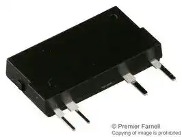
## **6. Slim SIL4-pin package**
(W) 3.5 × (D) 21.0 × (H) 12.5 mm
(W) .138 × (D) .827 × (H) .492 inch
The compact size of the 4-pin SIL package allows high density mounting.
## **TYPES**
## **1. DC type**
||Output ratin<br>Load voltage|ut rating*<br>Load current|Package|Part No.|Inner carton|Packing|quantity|Outer carton|
|---|---|---|---|---|---|---|---|---|
||60 V|3.6 A||AQZ102D|||||
|DC only|100 V<br>200 V|2.3 A<br>1.1 A|SIL4-pin|AQZ105D<br>AQZ107D|25 pcs.|||500 pcs.|
||400 V|0.6 A||AQZ104D|||||
|* Load voltage and current of DC type: DC||* Load voltage and current of DC type: DC|||||||
|**2. AC/DC type**|||||||||
||Output ratin<br>Load voltage|ut rating*<br>Load current|Package|Part No.|Inner carton|Packing|quantity|Outer carton|
||60 V|2.7 A||AQZ202D|||||
|AC/DC<br>dual use|100 V<br>200 V|1.8 A<br>0.9 A|SIL4-pin|AQZ205D<br>AQZ207D|25 pcs.|||500 pcs.|
||400 V|0.45 A||AQZ204D|||||
- Load voltage and current of DC type: DC
## **2. AC/DC type**
- Load voltage and current of AC/DC type: Peak AC/DC
ASCTB33E 201404-T
–1–
Power 1 Form A Voltage-sensitive (AQZ10❍D, 20❍D)
## **RATING**
## **1. DC type**
## 1) Absolute maximum ratings (Ambient temperature: 25°C 77°F)
||Item|Symbol|AQZ102D|AQZ105D|AQZ107D|AQZ104D|Remarks|
|---|---|---|---|---|---|---|---|
|Input|Input voltage|VIN|30 V|||||
||Input reverse voltage|VRIN|5 V|||||
||Power dissipation|Pin|300 mW|||||
|Output|Load voltage(DC)|VL|60 V|100 V|200 V|400 V||
||Continuous load current(DC)|IL|3.6 A|2.3 A|1.1 A|0.6 A||
||Peak load current|Ipeak|9.0 A|6.0 A|3.0 A|1.5 A|100 ms(1 shot), VL= DC|
||Power dissipation|Pout|1.35 W|||||
|Totalpower dissipation||PT|1.35 W|||||
|I/O isolation voltage||Viso|2,500 V AC|||||
|Temperature<br>limits|Operating|Topr|–40°C to +85°C–40°F to +185°F(4 VqVIN q6 V)<br>–40°C to +75°C–40°F to +167°F(6 V < VIN q15 V)<br>–40°C to +60°C–40°F to +140°F (15 V < VIN q30 V)||||Non-condensing at low<br>temperatures|
||Storage|Tstg|–40°C to +100°C–40°F to +212°F|||||
## 2) Electrical characteristics (Ambient temperature: 25°C 77°F)
||Item||Symbol|AQZ102D|AQZ105D|AQZ107D|AQZ104D|Remarks|
|---|---|---|---|---|---|---|---|---|
|Input|Operate voltage|Typical|VFon|1.4 V||||IL= 100 mA<br>VL= 10 V|
|||Maximum||4 V|||||
||Turn off voltage|Minimum|VFoff|0.8 V||||IL= 100 mA<br>VL= 10 V|
|||Typical||1.3 V|||||
||Input current|Typical|IIN|6.5 mA||||VIN= 5 V|
|Output|On resistance|Typical|Ron|0.033Ω|0.090Ω|0.33Ω|1.23Ω|VIN= 5 V<br>IL= Max.<br>Within 1 s on time|
|||Maximum||0.09Ω|0.17Ω|0.55Ω|1.6Ω||
||Off state leakage current|Maximum|ILeak|10μA||||VIN= 0 V<br>VL= Max.|
|Transfer<br>characteristics|Turn on time*|Typical|Ton|3.3 ms|2.2 ms|1.5 ms|1.2 ms|VIN= 5 V<br>IL= 100 mA<br>VL= 10 V|
|||Maximum||10.0 ms|||||
||Turn off time*|Typical|Toff|0.2 ms||0.1 ms||VIN= 5 V<br>IL= 100 mA<br>VL= 10 V|
|||Maximum||3.0 ms|||||
||I/O capacitance|Typical|Ciso|0.8pF||||f = 1 MHz<br>VB= 0 V|
|||Maximum||1.5pF|||||
||Initial I/O isolation resistance|Minimum|Riso|1,000 MΩ||||500 V DC|
||Maximum operating speed|Maximum|—|0.5 cps||||VIN= 5 V<br>Duty factor = 50%<br>IL×VL= 200(VA)|
|Vibration resistance||Minimum|—|10 to 55 Hz at double amplitude of 3 mm||||2 hours for 3 axes|
|Shock resistance||Minimum|—|4,900 m/s2 {500 G}1 ms||||3 times for 3 axes|
## **2. AC/DC type**
## 1) Absolute maximum ratings (Ambient temperature: 25°C 77°F)
||Item|Symbol|AQZ202D|AQZ205D|AQZ207D|AQZ204D|Remarks|
|---|---|---|---|---|---|---|---|
|Input|Input voltage|VIN|30 V|||||
||Input reverse voltage|VRIN|5 V|||||
||Power dissipation|Pin|300 mW|||||
|Output|Load voltage(peak AC)|VL|60 V|100 V|200 V|400 V||
||Continuous load current|IL|2.7 A|1.8 A|0.9 A|0.45 A|Peak AC, DC|
||Peak load current|Ipeak|9.0 A|6.0 A|3.0 A|1.5 A|100 ms(1 shot), VL= DC|
||Power dissipation|Pout|1.6 W|||||
|Totalpower dissipation||PT|1.6 W|||||
|I/O isolation voltage||Viso|2,500 V AC|||||
|Temperature<br>limits|Operating|Topr|–40°C to +85°C–40°F to +185°F(4 VqVIN q6 V)<br>–40°C to +75°C–40°F to +167°F(6 V < VIN q15 V)<br>–40°C to +60°C–40°F to +140°F (15 V < VIN q30 V)||||Non-condensing at low<br>temperatures|
||Storage|Tstg|–40°C to +100°C–40°F to +212°F|||||
ASCTB33E 201404-T
–2–
Power 1 Form A Voltage-sensitive (AQZ10❍D, 20❍D)
## 2) Electrical characteristics (Ambient temperature: 25°C 77°F)
||Item||Symbol|AQZ202D|AQZ205D|AQZ207D|AQZ204D|Remarks|
|---|---|---|---|---|---|---|---|---|
|Input|Operate voltage|Typical<br>Maximum|VFon|1.4 V||||IL= 100 mA<br>VL= 10 V|
|||||4 V|||||
||Turn off voltage|Minimum<br>Typical|VFoff|0.8 V||||IL= 100 mA<br>VL= 10 V|
|||||1.3 V|||||
||Input current|Typical|IIN|6.5 mA||||VIN= 5 V|
|Output|On resistance|Typical<br>Maximum|Ron|0.066Ω|0.180Ω|0.64Ω|2.4Ω|VIN= 5 V<br>IL= Max.<br>Within 1 s on time|
|||||0.18Ω|0.34Ω|1.1Ω|3.2Ω||
||Off state leakage current|Maximum|ILeak|10μA||||VIN= 0 V<br>VL= Max.|
|Transfer<br>characteristics|Turn on time*|Typical<br>Maximum|Ton|5.8 ms|4.2 ms|2.7 ms|2.3 ms|VIN= 5 V<br>IL= 100 mA<br>VL= 10 V|
|||||10.0 ms|||||
||Turn off time*|Typical<br>Maximum|Toff|0.2 ms||0.1 ms||VIN= 5 V<br>IL= 100 mA<br>VL= 10 V|
|||||3.0 ms|||||
||I/O capacitance|Typical<br>Maximum|Ciso|0.8pF||||f = 1 MHz<br>VB= 0 V|
|||||1.5pF|||||
||Initial I/O isolation resistance|Minimum|Riso|1,000 MΩ||||500 V DC|
||Maximum operating speed|Maximum|—|0.5 cps||||VIN= 5 V<br>Duty factor = 50%<br>IL×VL= 200(VA)|
|Vibration resistance||Minimum|—|10 to 55 Hz at double amplitude of 3 mm||||2 hours for 3 axes|
|Shock resistance||Minimum|—|4,900 m/s2 {500 G}1 ms||||3 times for 3 axes|
**==> picture [185 x 80] intentionally omitted <==**
**----- Start of picture text -----**<br>
*Turn on/off time<br>Input<br>90%<br>Output 10%<br>Ton Toff<br>**----- End of picture text -----**<br>
## **RECOMMENDED OPERATING CONDITIONS**
Please obey the following conditions to ensure proper device operation and resetting.
|Item|Symbol|Recommended value|Unit|
|---|---|---|---|
|Input voltage|VIN|5|V|
## ■ **These products are not designed for automotive use.**
**If you are considering to use these products for automotive applications, please contact your local Panasonic Corporation technical representative.**
## **REFERENCE DATA**
1. Load current vs. ambient temperature characteristics
Allowable ambient temperature: –40°C to +85°C –40°F to +185°F; VIN: Input voltage; IL (derate):Load current (derate); IL: Absolute maximum ratings of continuous load current
2.-(1) Load current vs. ambient temperature characteristics in adjacent mounting
Input voltage: 4V q VIN q 6V; IL (derate): Load current (derate); IL: Absolute maximum ratings of continuous load current; : Adjacent mounting pitch
2.-(2) Load current vs. ambient temperature characteristics in adjacent mounting
Input voltage: 6V < VIN q 15V; IL (derate): Load current (derate); IL: Absolute maximum ratings of continuous load current; : Adjacent mounting pitch
**==> picture [502 x 125] intentionally omitted <==**
**----- Start of picture text -----**<br>
120 100 100<br>100 80 =20mm =10mm 80 =20mm =10mm<br> 4V VIN 6V = 5mm = 5mm<br>80 6V<VIN 15V<br>15V<VIN 30V<br>60 60<br>60<br>40 40<br>40<br>20 20<br>20<br>0 0 0<br>–40 –20 0 20 40 60 8085 100 –40 –20 0 20 40 60 80 85 100 –40 –20 0 20 40 60 7580 100<br>Ambient temperature, °C Ambient temperature, °C Ambient temperature, °C<br> 100, %<br> 100, %× 100, %× ×<br>IL IL IL<br> (derate) IL (derate) IL (derate) IL<br>**----- End of picture text -----**<br>
ASCTB33E 201404-T
–3–
Power 1 Form A Voltage-sensitive (AQZ10❍D, 20❍D)
3.-(1) On resistance vs. ambient temperature characteristics (DC type)
## 3.-(2) On resistance vs. ambient temperature characteristics (DC type)
2.-(3) Load current vs. ambient temperature characteristics in adjacent mounting Input voltage: 15V<VIN q 30V; IL (derate): Load current (derate); IL: Absolute maximum ratings of continuous load current; : Adjacent mounting pitch
Input voltage: 5 V; Continuous load current: 3.6 A (DC) (AQZ102D) 2.3 A (DC) (AQZ105D)
Input voltage: 5 V; Continuous load current: 1.1 A (DC) (AQZ107D) 0.6 A (DC) (AQZ104D)
**==> picture [528 x 309] intentionally omitted <==**
**----- Start of picture text -----**<br>
100 0.25 5.0<br>80 0.20 4.0<br>=20mm<br>=10mm<br>= 5mm<br>60 0.15 3.0<br>AQZ105D<br>40 0.10 2.0<br>AQZ104D<br>20 0.05 AQZ102D 1.0<br>AQZ107D<br>0 0 0<br>–40 –20 0 20 40 60 80 100 –40 –20 0 20 40 60 80 85 –40 –20 0 20 40 60 80 85<br>Ambient temperature, °C Ambient temperature, °C Ambient temperature, °C<br>3.-(3) On resistance vs. ambient temperature 3.-(4) On resistance vs. ambient temperature 4.-(1) Turn on time vs. ambient temperature<br>characteristics (AC/DC type) characteristics (AC/DC type) characteristics (DC type)<br>Input voltage: 5 V; Input voltage: 5 V; Input voltage: 5 V; Load voltage: 10 V (DC);<br>Continuous load current: 2.7 A (DC) (AQZ202D) Continuous load current: 0.9 A (DC) (AQZ207D) Continuous load current: 100 mA (DC)<br>1.8 A (DC) (AQZ205D) 0.45 A (DC) (AQZ204D)<br>0.5 5.0 10<br>0.4 4.0 8<br>0.3 3.0 AQZ204D 6<br>AQZ205D AQZ102D<br>0.2 2.0 4<br>AQZ105D<br>0.1 AQZ202D 1.0 AQZ207D 2 AQZ107D<br>AQZ104D<br>0 0 0<br>–40 –20 Ambient temperature, 00 20 40 60 °C80C8080 85 –40 –20 Ambient temperature, 00 20 40 60 °C80C8080 85 –40 –20 Ambient temperature, 00 0 20 40 60°C°CC 808585<br>Ω<br>Ω<br> 100, %<br>×<br>IL<br> (derate) IL On resistance, On resistance,<br>On resistance, ΩΩ On resistance, ΩΩ Turn on time, ms<br>**----- End of picture text -----**<br>
**==> picture [528 x 487] intentionally omitted <==**
**----- Start of picture text -----**<br>
0.5 5.0 10<br>0.4 4.0 8<br>0.3 3.0 AQZ204D 6<br>AQZ205D AQZ102D<br>0.2 2.0 4<br>AQZ105D<br>0.1 AQZ202D 1.0 AQZ207D 2 AQZ107D<br>AQZ104D<br>0 0 0<br>–40 –20 Ambient temperature, 00 20 40 60 °C80C8080 85 –40 –20 Ambient temperature, 00 20 40 60 °C80C8080 85 –40 –20 Ambient temperature, 00 0 20 40 60°C°CC 808585<br>4.-(2) Turn on time vs. ambient temperature 5.-(1) Turn off time vs. ambient temperature 5.-(2) Turn off time vs. ambient temperature<br>characteristics (AC/DC type) characteristics (DC type) characteristics (AC/DC type)<br>Input voltage: 5 V; Input voltage: 5 V; Load voltage: 10 V (DC); Input voltage: 5 V; Load voltage: 10 V (DC);<br>Load voltage: 10 V (DC); Continuous load current: 100 mA (DC) Continuous load current: 100 mA (DC)<br>Continuous load current: 100 mA (DC)<br>10 0.5 0.5<br>8 0.4 0.4<br>AQZ202D<br>6 0.3 0.3<br>AQZ205D<br>4 0.2 AQZ107D 0.2<br>AQZ207D AQZ204D AQZ202D<br>AQZ102D<br>2 AQZ204D 0.1 AQZ104D AQZ105D 0.1 AQZ207D AQZ205D<br>0 0 0<br>–40 –20 0 20 40 60 8085 –40 –20 0 20 40 60 8085 –40 –20 0 20 40 60 80 85<br>Ambient temperature, °C Ambient temperature, °C Ambient temperature, °C<br>6. Operate voltage vs. ambient temperature 7. Turn off voltage vs. ambient temperature 8. Input current vs. ambient temperature<br>characteristics characteristics characteristics<br>Load voltage: 10 V (DC); Load voltage: 10 V (DC); Input voltage: 5 V<br>Continuous load current: 100 mA (DC) Continuous load current: 100 mA (DC)<br>5.0 5.0 10<br>4.0 4.0 8<br>3.0 3.0 6<br>2.0 2.0 4<br>1.0 1.0 2<br>0 0 0<br>–40 –20 0 20 40 60 8085 –40 –20 0 20 40 60 8085 –40 –20 0 20 40 60 8085<br>Ambient temperature, °C Ambient temperature, °C Ambient temperature, °C<br>On resistance, ΩΩ On resistance, ΩΩ<br>Turn on time, ms<br>Turn on time, ms Turn off time, ms Turn off time, ms<br>Operate voltage, V Turn off voltage, ms Input current, mA<br>**----- End of picture text -----**<br>
ASCTB33E 201404-T
–4–
Power 1 Form A Voltage-sensitive (AQZ10❍D, 20❍D)
## 9.-(1) Current vs. voltage characteristics of output at MOS portion (DC type) Ambient temperature: 25°C 77°F
9.-(2) Current vs. voltage characteristics of output at MOS portion (AC/DC type) Ambient temperature: 25°C 77°F
10. Input current vs. input voltage characteristics
Ambient temperature: 25°C 77°F
**==> picture [502 x 502] intentionally omitted <==**
**----- Start of picture text -----**<br>
4.0 AQZ102D 4.0 10<br>3.0 3.0 AQZ202D<br>AQZ105D 8<br>2.0 2.0 AQZ205D aa<br>1.0 AQZ107DAQZ104D | 1.0 | AQZ207DAQZ204D || 6<br>–0.8 –0.6 –0.4 –0.2 –2.0 –1.5 –1.0 –0.5 ye<br>0 0.2 0.4 0.6 0.8 0 0.5 1.0 1.5 2.0<br>–1.0 Voltage, V |TH –1.0 Voltage, V 4<br>| | |<br>–2.0 –2.0<br>–3.0 oeBRR –3.0 | 2<br>–4.0 –4.0 0<br>Pt tt 0 5 10 15 20 25 30<br>Input voltage, V<br>11.-(1) Off state leakage current vs. load 11.-(2) Off state leakage current vs. load 12. Maximum operating speed vs. load voltage<br>voltage characteristics voltage characteristics × load current characteristics load current characteristics<br>Ambient temperature: 25°C 77°F°C 77°FC 77°F77°F°FF Ambient temperature: 25°C 77°F Input voltage: 5V; Ambient temperature: 25°C 77°C 77C 7777°F<br>10<br>duty=50%<br>10 [–3] PtPtPt | ttttttT |tt|EETTTT|tTtT 10 [–3] PTP|Pt tTtttt tT|tt|TTttTtTytttT 987 ARSEryoteEEna<br>10 [–6] PEPEPeeeee 10 [–6] PEEPCCP eee errr 65 ASSASSIST<br>Pt ttt tT Tt tT P| tt tT | TT tT 4 FTE<br>10 [–9] AQZ105D,205D 10 [–9] AQZ104D,204D<br>=Pf ot ttyPer| Ppittierttt | 3 FAT<br>=> [>—] eee feet AQZ107D,207D 2 PINETt ttt<br>| 10 [–12] AQZ102D,202D 10 [–12] 1 | | tt |<br>A tN | me tT | tt Tt | P| SAL |<br>0 PTET Ey 50 et tt 100 0 PT TET 50 eT Tt 100 0 0 Pt 25 50 | 75 | Pr 100 125 150 175 200<br>Load voltage, V Load voltage, V Maximum voltage, V×Load current, A<br>13.-(1) Output capacitance vs. applied voltage 13.-(2) Output capacitance vs. applied voltage<br>characteristics (DC type) characteristics (AC/DC type)<br>Frequency: 1 MHz; Ambient temperature: 25°C 77°F°C 77°FC 77°F77°F°FF Frequency: 1 MHz; Ambient temperature: 25°C 77°F<br>2000 2000<br>1800 a 1800 a<br>1600 P| ET 1600 a<br>1400 Pt 1400 P| || |<br>1200 pf fT 1200 Pt [TT]<br>AQZ102D<br>1000 ee 1000 pot |<br>800 800<br>AQZ105D AQZ202D<br>600 i 600 eee<br>AQZ107D AQZ205D AQZ207D<br>Pn. 400 W oS AQZ104D | 400 We|r AQZ204D<br>200 200<br>0 0<br>0 20 40 60 80 100 0 20 40 60 80 100<br>Applied voltage, V Applied voltage, V<br>Current, A Current, A<br>Input current, mA<br>Off state leakage current, A Off state leakage current, A<br>Maximum operating speed, cps<br>Output capacitance, pF<br>Output capacitance, pF<br>**----- End of picture text -----**<br>
## 11.-(1) Off state leakage current vs. load voltage characteristics
12. Maximum operating speed vs. load voltage × load current characteristics load current characteristics
Ambient temperature: 25°C 77°F°C 77°FC 77°F77°F°FF
Input voltage: 5V; Ambient temperature: 25°C 77°C 77C 7777°F
## 13.-(1) Output capacitance vs. applied voltage characteristics (DC type)
Frequency: 1 MHz; Ambient temperature: 25°C 77°F°C 77°FC 77°F77°F°FF
## **ACCESSORY** (mm inch)
## **Socket**
**==> picture [467 x 155] intentionally omitted <==**
**----- Start of picture text -----**<br>
PC board pattern<br>1 2 3 4 5 6 .1975 [+0.2] –0.6 [±] –.024 [.008] 1 2 3 4 5 6 .1975 [+0.2] –0.6 [±] –.024 [.008] (BOTTOM VIEW)Standard type<br>22.6 [±][0.6] 22.6 [±][0.6] 5.08<br>.890 [±][.024] .890 [±][.024] 2.54 10.16 .200<br>.100 .400<br>9 [±][0.6] 9 [±][0.6] 2-1 dia. 2-1.2 dia.<br>.354 [±][.024] .354 [±][.024] 2-.039 dia. 2-.047 dia.<br>5.3.209 [±][0.6][±][.024] 5.3.209 [±][0.6][±][.024] Self clinching type<br>4 0.5 0.8 3.9 0.5 0.8 5.08<br>.157 ooEh .020 0.8.031 (.012)(0.3) 0.010.25 .039 1 [±][0.25][±][.010] .154 = .020 .031 (0.3)(.012) 2.54.100 1.4000.16 .200<br>Te 6.35.250.1002.54 3 .150.81 5.2.0800 ho .0481.23 of 1.23.048 JPical 6.35.2502.54.100 3 .150.81 5.20.080 a .0511.3 [±][0.15][±][.006] L oes 2-.0312-0.8 e [±][±][0.25 dia.][002 dia.] L 2-.0472-1.2 e [±][±][0.05 dia.][002 dia.]<br>PA1a-PS PA1a-PS-H Tolerance: ±0.1 ±.004<br>**----- End of picture text -----**<br>
ASCTB33E 201404-T
–5–
Updated at June 6, 2026
Panasonic Industry is a global leader in the design and manufacture of high-quality electronic components. Renowned for a commitment to continuous innovation, the company provides the essential building blocks that empower modern engineering. From industrial automation to consumer electronics, Panasonic's components are trusted worldwide for their outstanding reliability, efficiency, and long-term performance. The extensive portfolio is anchored by a massive selection of passive components, featuring an industry-leading range of aluminium electrolytic, film, and polymer capacitors. Alongside these advanced capacitance solutions, engineers rely on Panasonic's robust power inductors and a highly versatile array of electromechanical devices, including solid-state, power, and signal relays engineered to excel in demanding environments. Beyond core passives and switching solutions, the offering encompasses critical circuit protection devices such as TVS varistors and NTC thermistors, as well as sophisticated thermal management materials. Panasonic also delivers precision light and motion sensors, highly reliable batteries, and advanced Bluetooth and WLAN connectivity modules, providing a comprehensive ecosystem of components to support next-generation technological design.
About Novapart
Novapart is a B2B electronic component broker specialising in stock shortages and cost reduction. We source hard-to-find parts and identify compliant alternatives across a catalogue of 540,000+ components from 500+ manufacturers.
Learn more →Stock Shortage Specialist
When a component is unavailable, discontinued or has an unacceptable lead time, we tap into our network of vetted European and Asian distributors to source what you need — without compromising on quality or traceability.
Request a quote →Compliant Alternatives
We identify pin-to-pin, electrically equivalent substitutes that meet the same certifications (RoHS, AEC-Q100, REACH) as your original specification — validated against datasheets, not just part numbers. Often at a lower cost.
BOM Analysis service →