
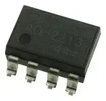


AQH1213AX
Solid State Relay, SPST-NO, 600 mA, 600 VAC, Surface Mount, Gull Wing, Zero Crossing
- Manufacturer: PANASONIC
- Product type:
- SVHC: To Be Advised
- Load Current: 600mA
- Product Range: AQ-H Series
- Relay Mounting: Surface Mount
- Switching Mode: Zero Crossing
- Relay Terminals: Gull Wing
- Control Voltage Max: -
- Control Voltage Min: -
- Contact Configuration: SPST-NO
- Operating Voltage Max: 600VAC
- Operating Voltage Min: -
| Delivery and price | |
|---|---|
| Units per pack | 100 |
| Price | 0.948 € |
| Current stock | 500+ |
| Lead time | 30 days |
**==> picture [97 x 43] intentionally omitted <==** ## Solid State Relays AQ-H RELAYS ## Product Catalog **==> picture [503 x 423] intentionally omitted <==** 2022.4 Solid State Relays ## AQ-H[ RELAYS] ## Compact DIP type SSR Ideal for AC load control ## ~~Pe FEATURES~~ - Supports 0.3 A, 0.6 A, 0.9 A and 1.2 A ONstate RMS currents. - ●Handles both 100 and 200 Vrms loads. - ●High dielectric strength: 5,000 Vrms - ●Safety standards **==> picture [186 x 59] intentionally omitted <==** **----- Start of picture text -----**<br> 1 − 8 1 − 8<br>+ +<br>2 2<br>3 − 6 3 − 6<br>ZC<br>4 − 5 4 − 5<br>Zero-cross circuit<br>**----- End of picture text -----**<br> - CUL ( UL1577 ) certified • VDE ( EN623681 ) reinforced insulation certified ## ~~Pe TYPICAL APPLICATIONS~~ - Home appliances market: air conditioner, microwave oven, washing machine, personal hygiene system, refrigerator, fan heater, inductive heating cooker, rice cooker and humidifier, etc. - ●Industrial equipment market ## ee **ORDERING INFORMATION ( PART NO. )** **AQH 2** TJ ON-state RMS current ~~Ca~~ Repetitive Type Number Package Packing 0: 0.3 A peak OFF-state voltage 1: Zero-cross of pin Nil: DIP Nil: Tube 1: 0.6 A 2: 600 V 2: Random 3: 8 pins S: SOP X: Tape and reel packing X 2: 0.9 A A: SMD 3: 1.2 A TYPES | Output rating Part No. Standard Packing Type Repetitive ONstate Method Through hole terminal Surfacemount terminal peak OFF RMS current Tube packing Tube packing Tape and reel Tube Tape and reel state voltage style style packing style X* ~~|~~ 0.3 A AQH0213 AQH0213A AQH0213AX 0.6 A AQH1213 AQH1213A AQH1213AX Zerocross 0.9 A AQH2213 AQH2213A AQH2213AX 1 tube contains: typeAC 600 V 1.2 A0.3 A AQH3213AQH0223 AQH3213AAQH0223A AQH3213AXAQH0223AX 1 batch contains: 50 pcs. 1,000 pcs. 0.6 A AQH1223 AQH1223A AQH1223AX 500 pcs. Random 0.9 A AQH2223 AQH2223A AQH2223AX ~~==~~ 1.2 A ~~ES~~ AQH3223 AQH3223A AQH3223AX Note: For space reasons, the SMD terminal shape indicator "A" and the package type indicator "X" are omitted from the seal. * Tape and reel packing style X: picked from the 1/2/3/4pin side. For part numbers with picked from the 5/6/8pin side, change the "X" at the end to "Z" when ordering. Panasonic Industry Co., Ltd. Electromechanical Control Business Division industrial.panasonic.com/ac/e/ ASCTB61E 202204 ー 1 ー Panasonic Industry Co., Ltd. 2022 Solid State Relays AQ-H RELAYS ## RATING ## ■Absolute maximum ratings ( Ambient temperature: 25℃ ) **==> picture [511 x 191] intentionally omitted <==** **----- Start of picture text -----**<br> AQH0213 AQH1213 AQH2213 AQH3213<br>Item Symbol Remarks<br>AQH0223 AQH1223 AQH2223 AQH3223<br>LED forward current IF 50 mA<br>LED reverse voltage VR 6 V<br>Peak forward f = 100 Hz,<br>IFP 1 A<br>current Duty Ratio = 0.1%<br>Repetitive peak OFF VDRM 600 V<br>state voltage<br>ONstate RMS<br>current IT(RMS) 0.3 A 0.6 A 0.9 A 1.2 A<br>Nonrepetitive surge current ITSM 3 A 6 A 9 A 12 A In one cycle at 60 Hz<br>I/O isolation voltage Viso 5,000 Vrms<br>Ambient temperature Topr 30 to +85℃ Nonicing and noncondensing<br>Storage temperature Tstg 40 to +125℃ Nonicing and noncondensing<br>Junction temperature Tj 125℃<br>Input<br>Output<br>**----- End of picture text -----**<br> Note: "A" and "AX" at the end of the part numbers have been omitted. ## ■Characteristics ( Ambient temperature: 25℃ ) **==> picture [512 x 240] intentionally omitted <==** **----- Start of picture text -----**<br> AQH0213, AQH1213 AQH0223, AQH1223<br>Item Symbol Remarks<br>AQH2213, AQH3213 AQH2223, AQH3223<br>Typical 1.21 V<br>LED dropout voltage VF IF = 20 mA<br>Maximum 1.3 V<br>Typical ー<br>LED reverse current IR VR = 6 V<br>Maximum 10 µA<br>Peak OFFstate Typical ー IF = 0 mA<br>IDRM<br>current Maximum 100 µA VDRM = 600 V<br>Peak ONstate Typical ー IF = 10 mA<br>VTM<br>voltage Maximum 2.5 V ITM = Max.<br>Typical ー<br>Holding current IH<br>Maximum 25 mA<br>Critical rate of rise of<br>OFFstate voltage Minimum dv/dt 200 V/µs VDRM = 600 V × 1/√2<br>VD = 6 V<br>Trigger LED current Maximum IFT 10 mA RL = 100 Ω<br>Zerocross voltage Maximum VZC 50 V ー IF = 10 mA<br>IF = 20 mA<br>Turn on time* Maximum Ton 100 µs VD = 6 V<br>RL = 100 Ω<br>I/O isolation<br>Minimum Riso 50 GΩ 500 V DC<br>resistance<br>Input<br>Output<br>Transfer characteristics<br>**----- End of picture text -----**<br> Notes: 1. For type of connection, see "SCHEMATIC AND WIRING DIAGRAMS". 2. "A" and "AX" at the end of the part numbers have been omitted. - Turn on/Turn off time **==> picture [153 x 81] intentionally omitted <==** **----- Start of picture text -----**<br> Input<br>Output<br>Ton<br>**----- End of picture text -----**<br> **==> picture [11 x 5] intentionally omitted <==** **----- Start of picture text -----**<br> 90%<br>**----- End of picture text -----**<br> ## ■Recommended operating conditions Please use under recommended operating conditions to obtain expected characteristics. |Item|Symbol|Min.|Max.|Unit| |---|---|---|---|---| |Input LED current|IF|15|25|mA| Panasonic Industry Co., Ltd. Electromechanical Control Business Division industrial.panasonic.com/ac/e/ ASCTB61E 202204 ー 2 ー Panasonic Industry Co., Ltd. 2022 Solid State Relays AQ-H RELAYS ## REFERENCE DATA **==> picture [168 x 382] intentionally omitted <==** **----- Start of picture text -----**<br> 3. Trigger LED current vs. ambient<br>temperature characteristics<br>Load voltage: 6 V DC;<br>Load resistance: 100 Ω<br>10<br>8<br>6<br>4<br>2<br>0<br>-40 -30 -20 0 20 40 60 80 100<br>Ambient temperature, °C<br>6. Repetitive peak OFFstate current vs.<br>load voltage characteristics<br>Ambient temperature: 25°C<br>Measured portion: between terminals 6 and 8; LED current: 0 mA<br>10 [[-3]]<br>10 [[-4]]<br>10 [[-5]]<br>10 [[-6]]<br>10 [[-7]]<br>10 [[-8]]<br>10 [[-9]]<br>10 [[-10]]<br>0 20 40 60 80 100<br>Load voltage, V<br>Trigger LED current, mA<br>Repetitive peak OFF-state current, A<br>**----- End of picture text -----**<br> 1. ONstate RMS current vs. ambient temperature characteristics 2. Peak ONstate voltage vs. ambient temperature characteristics **==> picture [113 x 7] intentionally omitted <==** **----- Start of picture text -----**<br> Allowable ambient temperature: –30 to +85°C<br>**----- End of picture text -----**<br> **==> picture [511 x 554] intentionally omitted <==** **----- Start of picture text -----**<br> Allowable ambient temperature: –30 to +85°C LED current: 10 mA; ON current: Max. Load voltage: 6 V DC;<br>Measured portion: between terminals 6 and 8 Load resistance: 100 Ω<br>1.5 1.6 10<br>1.2 AQH3213, AQH3223 1.4 8<br>AQH0213, AQH0223<br>0.9 AQH2213, AQH2223 1.2 AQH1213, AQH1223 6<br>0.6 AQH1213, AQH1223 1 AQH2213, AQH2223 4<br>AQH3213, AQH3223<br>0.3 AQH0213, AQH0223 0.8 2<br>0 0.6 0<br>-40 -30 -20 0 20 40 60 8085 100 -40 -30 -20 0 20 40 60 80 100 -40 -30 -20 0 20 40 60 80 100<br>Ambient temperature, °C Ambient temperature, °C Ambient temperature, °C<br>4. LED dropout voltage vs. ambient 5. Turn on time vs. LED current 6. Repetitive peak OFFstate current vs.<br>temperature characteristics characteristics load voltage characteristics<br>LED current: 10 to 50 mA Load voltage: 6 V DC; Load resistance: 100 Ω Ambient temperature: 25°C<br>Measured portion: between terminals 6 and 8 Measured portion: between terminals 6 and 8; LED current: 0 mA<br>1.5 100 10 [[-3]]<br>10 [[-4]]<br>1.4 80<br>10 [[-5]]<br>1.3 60 10 [[-6]]<br>50 mA<br>10 [[-7]]<br>1.2 40<br>30 mA<br>20 mA 10 [[-8]]<br>1.1 10 mA 20<br>10 [[-9]]<br>1 0 10 [[-10]]<br>-40 -30 -20 0 20 40 60 80 100 0 10 20 30 40 50 0 20 40 60 80 100<br>Ambient temperature, °C Trigger LED current, mA Load voltage, V<br>7. Holding current vs. ambient 8. Zerocross voltage vs. ambient<br>temperature characteristics temperature characteristics<br>LED current: 10 mA<br>25 50<br>20 40<br>AQH0213, AQH1213, AQH2213, AQH3213<br>15 30<br>AQH1213, AQH1223<br>AQH2213, AQH2223<br>10 20<br>5 10<br>AQH0213, AQH0223<br>AQH3213, AQH3223<br>0 0<br>-40 -30 -20 0 20 40 60 80 100 -40 -30 -20 0 20 40 60 80 100<br>Ambient temperature, °C Ambient temperature, °C<br>Trigger LED current, mA<br>ON-state RMS current, A Peak ON-state voltage, V<br>Turn on time, μs<br>LED dropout voltage, V<br>Repetitive peak OFF-state current, A<br>Hold current, mA<br>Zero-cross voltage, V<br>**----- End of picture text -----**<br> Panasonic Industry Co., Ltd. Electromechanical Control Business Division industrial.panasonic.com/ac/e/ ASCTB61E 202204 ー 3 ー Panasonic Industry Co., Ltd. 2022 Solid State Relays AQ-H RELAYS > **CAD** The CAD data of the products with a "CAD" mark can be downloaded from our Website. Unit: mm ## ~~a~~ DIMENSIONS ■Surface-mount terminal type ■Through hole terminal type ## **CAD** **==> picture [499 x 187] intentionally omitted <==** **----- Start of picture text -----**<br> External dimensions CAD External dimensions<br>MAX.10°<br>MAX.10°<br>MAX.10°<br>Recommended<br>PC board pattern 9.78 3.4<br>mounting pad<br>( BOTTOM VIEW )<br>( TOP VIEW )<br>7-0.8 dia. hole<br>7.62 eo t 9.78 ag 3.4<br>2.54<br>0.5 0.5<br>0.5 0.5<br>1.2 1.2 0.5 0.5<br>1.2 1.2 0.5 0.5<br>2.54<br>1.2 1.2<br>2.54 2.54 Terminal thickness: 0.25 1.5 1.2 1.2<br>eae Tolerance: ±0.1 General tolerance: ± 0.1 2.54 iain 2.54 2.54 ini 2.54 2.54 tf 2.54 Terminal thickness: 0.25<br>Tolerance: ±0.1 General tolerance: ± 0.1<br>6.4 7.62<br>3.9 ± 0.2 6.4 7.62<br>1<br>3.0<br>3.4<br>8.3<br>6.4 7.62 +0.2 0−<br>0.2<br>2.54 1.9<br>**----- End of picture text -----**<br> ## Po SCHEMATIC AND WIRING DIAGRAMS **==> picture [426 x 215] intentionally omitted <==** **----- Start of picture text -----**<br> Schematic pT confiOutputguration Load Wiring diagram<br>1 8 Load<br>1 −+ +i 8 Powersource atinput side RIN 23 6 Loadpowersupply<br>2 4 5<br>3 − ZC 6 1 8<br>4 − 5 Power RIN 2 7 Loadpower<br>Zero-cross circuit source atinput side 3 6 Load supply<br>4 5<br>1 Form A AC<br>1 8 Load<br>1- 8 Power RIN 2 Loadpower<br>2+ source atinput side 3 6 supply<br>4 5<br>3- 6<br>4- 5 Power RIN 12 87 Loadpower<br>source atinput side 3 6 Load supply<br>4 5<br>**----- End of picture text -----**<br> ## ~~Lo~~ SAFETY STANDARDS |Type|Type|UL(Recognized)<br>File No.<br>(Standard No.)<br>Contact rating|UL(Recognized)<br>File No.<br>(Standard No.)<br>Contact rating|CSA(Certified)|CSA(Certified)|VDE(Certified)|VDE(Certified)|Remarks| |---|---|---|---|---|---|---|---|---| ||||Contact rating|File No.<br>(Standard No.)|Contact<br>rating|File No.<br>(Standard No.)|Contact rating<br>(Reinforced insulation)|| |AQH|0.3 A type<br>0.6 A type<br>0.9 A type<br>1.2 A type|0.3 A type<br>0.6 A type<br>0.9 A type<br>1.2 A type<br>E191218<br>( UL1577 )|0.3 A 600 V AC ( peak )<br>0.6 A 600 V AC ( peak )<br>0.9 A 600 V AC ( peak )<br>1.2 A 600 V AC ( peak )|( Certified by CUL )||Nr. 40004928<br>( EN623681 )|0.3 A 520 V AC ( peak )<br>0.6 A 520 V AC ( peak )<br>0.9 A 520 V AC ( peak )<br>1.2 A 520 V AC ( peak )|VDE ( Basic insulation )<br>0.3 A 600 V AC ( peak )<br>0.6 A 600 V AC ( peak )<br>0.9 A 600 V AC ( peak )<br>1.2 A 600 V AC( peak)| Note: For the latest information on compliance with safety standards, please refer to our website. Please refer to "the latest product specifications" when designing your product. •Requests to customers: https://industrial.panasonic.com/ac/e/salespolicies/ Panasonic Industry Co., Ltd. Electromechanical Control Business Division industrial.panasonic.com/ac/e/ ASCTB61E 202204 ー 4 ー Panasonic Industry Co., Ltd. 2022 **Cautions for Use of Solid State Rela s y** ## **SAFETY WARNINGS** - Do not use the product under conditions that exceed the range of its specifications. It may cause overheating, smoke, or fire. - Do not touch the recharging unit while the power is on. There is a danger of electrical shock. - Check the connection diagrams in the catalog and be sure to connect the terminals correctly. If the device is energized with short circuit or any wrong connection, it may cause unexpected malfunction, abnormal heat or fire. - Be sure to turn off the power when performing mounting, maintenance, or repair operations on the relay (including connecting parts such as the terminal board and socket). ## **Cautions for Use of Solid State Relays** ## **Derating design** Derating is a significant factor for reliable design and product life. Even if the conditions of use (temperature, current, voltage, etc.) of the product are within the absolute maximum ratings, reliability may be lowered remarkably when continuously used in high load conditions (high temperature, high humidity, high current, high voltage, etc.) Therefore, please derate sufficiently below the absolute maximum ratings and evaluate the device in the actual condition. - Moreover, regardless of the application, if malfunctioning can be expected to pose high risk to human life or to property, or if products are used in equipment otherwise requiring high operational safety, in addition to designing double circuits, that is, incorporating features such as a protection circuit or a redundant circuit, safety testing should also be carried out. ## **Applying stress that exceeds the absolute maximum rating** - If the voltage or current value for any of the terminals exceeds the absolute maximum rating, internal elements will deteriorate because of the overvoltage or overcurrent. In extreme cases, wiring may melt, or silicon P/N junctions may be destroyed. Therefore, the circuit should be designed in such a way that the load never exceed the absolute maximum ratings, even momentarily. ## **Phototriac coupler** The phototriac coupler is designed solely to drive a triac. As a condition, the triac must be powered beforehand. ## **Unused terminals** - 1) Phototriac coupler The No. 3 terminal is used with the circuit inside the device. Therefore, do not connect it to the external circuitry. (6 pins) - 2) AQ-H The No. 5 terminal is connected to the gate. Do not directly connect No. 5 and 6 terminals. ## **Short across terminals** Do not short circuit between terminals when device is energized, since there is possibility of breaking of the internal IC. ## **When used for the load less than rated** An SSR may malfunction if it is used below the specified load. In such an event, use a dummy resistor in parallel with the load. **==> picture [140 x 60] intentionally omitted <==** **----- Start of picture text -----**<br> Ro (dummy resistor)<br>1<br>Load<br>SSR<br>2<br>supply<br>Load power<br>**----- End of picture text -----**<br> ## **Load Specifications** **==> picture [245 x 73] intentionally omitted <==** **----- Start of picture text -----**<br> Type Load current<br>AQ-G All models 20 mA<br>AQ1 All models 50 mA<br>AQ8 All models 50 mA<br>AQ-J All models 50 mA<br>AQ-A (AC output type) 100 mA<br>**----- End of picture text -----**<br> ## **Noise and surge protection at the input side** ## **1) Phototriac coupler and AQ-H** If reverse surge voltages are present at the input terminals, connect a diode in reverse parallel across the input terminals and keep the reverse voltages below the reverse breakdown voltage. Typical circuits are below shown. < Phototriac coupler (6-pin)> |||||||| |---|---|---|---|---|---|---| |||||1||6<br>5<br>4| |||||2||| |||||||| |||||||| |||||||| |||||3||| |||||||| ## **2) SSR** A high noise surge voltage applied to the SSR input circuit can cause malfunction or permanent damage to the device. If such a high surge is anticipated, use C or R noise absorber in the input circuit. Typical circuits are below shown **==> picture [144 x 60] intentionally omitted <==** **----- Start of picture text -----**<br> R<br>3<br>+− C SSR<br>4<br>source<br>Control voltage<br>**----- End of picture text -----**<br> ## **Recommended input current of Phototriac coupler and AQ-H** Design in accordance with the recommended operating conditions for each product. Since these conditions are affected by the operating environment, ensure conformance with all relevant specifications. ## **Ripple in the input power supply** If ripple is present in the input power supply, observe the following: ## **1) Current-sensitive type (Phototriac Coupler, AQ-H)** - (1) For LED forward current at Emin, please maintain the value mentioned at “Recommended input current.” - (2) Please make sure the LED forward current for Emax. is no higher than 50 mA. ## **2) Voltage-sensitive type (AQ-G, AQ1, AQ8, AQ-J, AQ-A)** - (1) The Emin. should exceed the minimum rated control voltage - (2) The Emax. should not exceed the maximum rated control voltage **==> picture [156 x 44] intentionally omitted <==** **----- Start of picture text -----**<br> Emin. Emax.<br>**----- End of picture text -----**<br> ## **When the input terminals are connected with reverse polarity** **==> picture [246 x 72] intentionally omitted <==** **----- Start of picture text -----**<br> Product name If the polarity of the input control voltage is reversed<br>AQ1, AQ-J, Reversing the polarity will not cause damage to the<br>device, due to the presence of a protection diode, but<br>AQ-A (AC) the device will not operate.<br>AQ-H, AQ-G, Reversing the polarity may cause permanent damage to<br>AQ8, AQ-A the device. Take special care to avoid polarity reversal or<br>(DC) use a protection diode in the input circuit.<br>**----- End of picture text -----**<br> Panasonic Industry Co., Ltd. Electromechanical Control Business Division industrial.panasonic.com/ac/e/ ASCTB400E 202204 Panasonic Industry Co., Ltd. 2022 ー 5 ー Cautions for Use of Solid State Relays ## **Noise and surge protection at the output side** ## **1) Phototriac coupler and AQ-H** The figure below shows an ordinary triac drive circuit. Please add a snubber circuit or varistor, as noise/surge on the load side could damage the unit or cause malfunctions. Typical circuits are shown below. ## **<Phototriac coupler SOP4 and DIP4 types>** **==> picture [139 x 51] intentionally omitted <==** **----- Start of picture text -----**<br> 1 4 Load<br>U<br>2 3<br>**----- End of picture text -----**<br> ## **<Phototriac coupler DIP6 type>** **==> picture [177 x 142] intentionally omitted <==** **----- Start of picture text -----**<br> 1 6 Load<br>2<br>U<br>3 4<br><AQ-H><br>1 8 Load<br>2<br>U<br>3 6<br>4 5<br>Note: Connection of an external resister, etc.,<br>to terminal No. 5 (gate) is not necessary.<br>**----- End of picture text -----**<br> ## **2) SSR** ## **(1) AC output type** A high noise surge voltage applied to the SSR load circuit can cause malfunction or permanent damage to the device. If such a high surge is anticipated, use a varistor across the SSR output. **==> picture [261 x 155] intentionally omitted <==** **----- Start of picture text -----**<br> 1<br>Load<br>SSR<br>V<br>2<br> Varistor<br>(2) DC output type<br>If an inductive load generates spike voltages which exceed the<br>absolute maximum rating, the spike voltage must be limited.<br>Typical circuits are shown below.<br>SSR SSR<br>V<br>Load Load<br>supply<br>Load power<br>Load power supply Load power supply<br>**----- End of picture text -----**<br> - **Cleaning (for PC board mounting type)** Cleaning the solder flux should use the immersion washing with an organic solvent. If you have to use ultrasonic cleaning, please adopt the following conditions and check that there are no problems in the actual usage. - Frequency : 27 to 29kHz - Ultrasonic output: No greater than 0.25W/cm[2] (Note) Cleaning time : 30s or less - Others : Float PC board and the device in the cleaning solvent to prevent from contacting the ultrasonic vibrator. Note: Applies to unit area ultrasonic output for ultrasonic baths ## **Notes for mounting (for PC board mounting type)** - **1) When different kinds of packages are mounted on PC board, temperature rise at soldering lead is highly dependent on package size. Therefore, please set the lower temperature soldering condition than the conditions of item “14. Soldering”, and confirm the temperature condition of actual usage before soldering.** - **2) When mounting condition exceeds our recommendation, the device characteristics may be adversely affected. It may occur package crack or bonding wire breaking because of thermal expansion unconformity and resin strength reduction. Please contact our sales office about the propriety of the condition.** - **3) Please confirm the heat stress by using actual board because it may be changed by board condition or manufacturing process condition** - **4) Solder creepage, wettability, or soldering strength will be affected by the mounting condition or used soldering type. Please check them under the actual production condition in detail.** - **5) Please apply coating when the device returns to a room temperature.** - **3) Clamp diode and snubber circuit can limit spike voltages at** - **the load side. However, long wires may cause spike voltages due to inductance. It is recommended to keep wires as short as possible to minimize inductance.** - **4) Output terminals may become conductive although the input power is not applied, when a sudden voltage rise is applied to it even when the relay is off. This may occur even if voltage rise between terminals is less than the repetitive peak OFF-state voltage. Therefore, please perform sufficient tests with actual conditions.** - **5) When controlling loads in which the voltage and current phases differ, a sudden voltage rise is applied during turnoff, and the triac sometimes does not turn off. Please conduct sufficient tests using actual equipment.** - **6) When controlling loads using zero-cross voltage types in which the voltage and current phases differ, the triac sometimes does not turn on regardless of the input state, so please conduct sufficient tests using actual equipment.** Panasonic Industry Co., Ltd. Electromechanical Control Business Division industrial.panasonic.com/ac/e/ ASCTB400E 202204 ー 6 ー Panasonic Industry Co., Ltd. 2022 Cautions for Use of Solid State Relays ## **Soldering** ## **1) When soldering surface-mount terminals, the following conditions are recommended.** ## (1) IR (Infrared reflow) soldering method (Recommended condition reflow: Max. 2 times, measurement point: soldering lead) t3 T3 T1 = 150 to 180°C T2 T2 = 230°C T3 = 240 to 250°C T1 t1 = 60 to 120 s t2 = Within 30 s t3 = Within 10 s t1 t2 - (2) Other soldering methods Other soldering methods (VPS, hot-air, hot plate, laser heating, pulse heater, etc.) affect the relay characteristics differently, please evaluate the device under the actual usage. ## (3) Soldering iron method Tip temperature: 350 to 400 °C Wattage : 30 to 60 W Soldering time : within 3 s ## **2) When soldering standard PC board terminals, the following conditions are recommended.** ## (1) DWS soldering method (Recommended condition number of times: Max. 1 time, measurement point: soldering lead *1) **==> picture [216 x 75] intentionally omitted <==** **----- Start of picture text -----**<br> T 2 T1 = 120°C<br>T2 = Max. 260°C<br>t1 = within 60 s<br>T 1<br>t2+t3 = within 5 s<br>t 1 t 2 t 3<br>**----- End of picture text -----**<br> - *1 Solder temperature: Max. 260 °C ## **Transportation and storage** - **1) Extreme vibration during transport may deform the lead or damage the device characteristics. Please handle the outer and inner boxes with care.** - **2) Inadequate storage condition may degrade soldering, appearance, and characteristics. The following storage conditions are recommended:** - Temperature: 0 to 45 °C - Humidity: Max. 70%RH - Atmosphere: No harmful gasses such as sulfurous acid gas, minimal dust. - **3) Storage of Phototriac coupler (SOP type)** - In case the heat stress of soldering is applied to the device which absorbs moisture inside of its package, the evaporation of the moisture increases the pressure inside the package and it may cause the package blister or crack. This device is sensitive to moisture and it is packed in the sealed moisture-proof package. Please make sure the following condition after unsealing. Please use the device immediately after unsealing. - (Within 30 days at 0 to 45 °C and Max. 70%RH) - If the device will be kept for a long time after unsealing, please store in the another moisture-proof package containing silica gel. (Please use within 90 days.) ## **Water condensation** - Water condensation occurs when the ambient temperature changes suddenly from a high temperature to low temperature at high humidity, or the device is suddenly transferred from a low ambient temperature to a high temperature and humidity. Condensation causes the failures such as insulation deterioration. Panasonic Industry Co., Ltd. does not guarantee the failures caused by water condensation. The heat conduction by the equipment the SSR is mounted may accelerate the water condensation. Please confirm that there is no condensation in the worst condition of the actual usage. (Special attention should be paid when high temperature heating parts are close to the SSR.) - (2) Other dip soldering method (recommended condition: 1 time) Preheating: Max. 120 °C, within 120 s, measurement point: - soldering lead Soldering: Max. 260 °C, within 5 s*, measurement area: soldering temperature - *Phototriac coupler and AQ-H: within 10 s - (3) Manual soldering method Tip temperature: 350 to 400°C Wattage: 30 to 60 W Soldering time: within 3 s We recommend one with an alloy composition of Sn3.0Ag0.5Cu. ## **Others** - **1) If an SSR is used in close proximity to another SSR or heat-generating device, its ambient temperature may exceed the allowable level. Carefully plan SSR layout and ventilation.** - **2) Terminal connections should be made by referring to the associated wiring diagram.** ## **3) For higher reliability, check device quality under actual operating conditions.** - **4) To prevent the danger of electrocution, turn off the power supply when performing maintenance. Although AQ-A (DC output type) is constructed with insulation for the input/ output terminals and the rear aluminum plate, the insulation between the input/output and the rear aluminum plate is not UL approved.** Panasonic Industry Co., Ltd. Electromechanical Control Business Division industrial.panasonic.com/ac/e/ ASCTB400E 202204 Panasonic Industry Co., Ltd. 2022 ー 7 ー Cautions for Use of Solid State Relays ## **The following shows the packaging format** **==> picture [511 x 614] intentionally omitted <==** **----- Start of picture text -----**<br> 1) Tape and reel (Phototriac coupler)<br>Type Tape dimensions (Unit: mm) Dimensions of paper tape reel (Unit: mm)<br>Direction of picking 21 [±][0.8]<br>Tractor feed holes 80 [±][1] dia.<br>0.3 [±][0.05] 1.5 +0.1ー0 dia. 7.2 ±0.1<br>2 [±][0.5]<br>SO package Device mounted on tape<br>4-pin type 2.8 [±][0.3] 4 [±][0.1] 1.55 [±][0.1] dia.<br>12 [±][0.1] 2 [±][0.1]<br>(1) When picked from 1/2-pin side: Part No. APT****SX<br>(Shown above)<br>(2) When picked from 3/4-pin side: Part No. APT****SZ *Quality of material: Paper 13 [±][0.5] dia. 14±1.5 2 [±][0.5]<br>21 [±][0.8]<br>80 [±][1] dia.<br>Direction of picking<br>Tractor feed holes<br>0.3 ±0.05 1.5+0.1ー0 dia. 4 [±][0.1] 10.2 [±][0.1] 2 [±][0.5]<br>DIP<br>Device mounted on tape<br>4-pin type 12 [±][0.1] 2 [±][0.1] 1.55 [±][0.1] dia.<br>4.2 [±][0.3]<br>(1) When picked from 1/2-pin side: Part No. APT****AX<br>(2) When picked from 3/4-pin side: Part No. APT****AZ *Quality of material: Paper 13 [±][0.5] dia. 13.5 [±][2.0] 2±0.5<br>21±0.8<br>Direction of picking 80 [±][1] dia.<br>Tractor feed holes<br>0.3 [±0.05] 1.5 +0.1- 0 dia. 10.1 ±0.1<br>2±0.5<br>DIP Device mounted<br>6-pin type on tape<br>12 [±0.1] 4 [±0.1] 1.6 ±0.1 dia.<br>4.5 [±0.3]<br>2 [±0.1]<br>(1) When picked from 1/2/3-pin side: Part No. APT****AX<br>(2) When picked from 4/5/6-pin side: Part No. APT****AZ *Quality of material: Paper 13±0.5dia. 17.5 [±][2] 2 [±][0.5]<br>0.35 [±0.05] Tractor feed holes1.5 +0.1- 0 dia. 4.0Direction of picking±0.1 9.2 [±0.1] 21±0.8100 [±][1] dia.<br>2 [±][0.5]<br>DIP<br>6-pin wide Device mounted<br>terminal type on tape<br>4.3 [±0.3] 12.0 [±0.1] 2.0 [±0.1] 1.6 ±0.1 dia.<br>(1) When picked from 1/6-pin side: Part No. APT****WAY<br>(2) When picked from 3/4-pin side: Part No. APT****WAW *Quality of material: Paper 13 [±][0.5] dia. 25.5 [±][2] 1.7 [±][0.8]<br>0.1±<br>1.75<br>0.1±4.7 0.1±5.5 +0.3120.1ー<br>±dia.1 2±dia.<br>80 250<br>0.1±1.75<br>0.1±5.25 0.1±5.5 +0.3120.1ー ±1dia. 2±dia.<br>80 300<br>±0.1<br>1.75<br>±0.1<br>±0.19.2 7.5 +0.361 0.1- ±1dia. 2±dia.<br>80 300<br>±0.1<br>1.75<br>±0.1<br>11.5 ±0.3<br> ±0.112.1 4.02 ±1dia. 2±dia.<br>100 330<br>**----- End of picture text -----**<br> Panasonic Industry Co., Ltd. Electromechanical Control Business Division industrial.panasonic.com/ac/e/ ー 8 ー ASCTB400E 202204 Panasonic Industry Co., Ltd. 2022 Cautions for Use of Solid State Relays ## **2) Tape and reel (AQ-H)** **==> picture [511 x 161] intentionally omitted <==** **----- Start of picture text -----**<br> Type Tape dimensions (Unit: mm) Dimensions of paper tape reel (Unit: mm)<br>Direction of picking 21±0.8<br>0.3 [±0.05] Tractor feed holes1.5 +0.1- 0 dia. 4 ±0.1 10.1 ±0.1 80 [±][1] dia.<br>2±0.5<br>8-pin SMD Device mounted<br>on tape<br>type 12 [±0.1] 2 [±0.1] 1.55±0.1dia.<br>4.5 [±0.3]<br>(1) When picked from 1/2/3/4-pin side: Part No. AQH****AX<br>(Shown above)<br>(2) When picked from 5/6/8-pin side: Part No. AQH****AZ *Quality of material: Paper 13±0.5dia. 17.5 [±][2] 2 [±][0.5]<br>±0.1<br>75<br>1.<br>±0.1<br>±0.1 7.5 +0.3 0.1-<br>10.2 16 ±1dia. 2±dia.<br>80 300<br>**----- End of picture text -----**<br> ## **3) Tube** Phototriac coupler and AQ-H SSR are packaged in a tube as pin No. 1 is on the stopper B side. Observe correct orientation when mounting them on PC boards. <Phototriac coupler SOP type> Stopper B (green) Stopper A (gray) <Phototriac coupler DIP type and AQ-H SSR> Stopper Panasonic Industry Co., Ltd. Electromechanical Control Business Division industrial.panasonic.com/ac/e/ ー 9 ー > Panasonic Industry Co., Ltd. 2022 ASCTB400E 202204 Cautions for Use of Solid State Relays ## **Snubber Circuit** ## **Reduce dv/dt** An SSR used with an inductive load can accidentally fire due to a high load voltage rise rate (dv/dt), even though the load voltage is below the allowable level (inductive load firing). Our SSRs contain a snubber circuit designed to reduce dv/dt (except AQ-H). ## **Selecting the snubber constants** ## **1) C selection** The charging coefficient tau for C of the SSR circuit is shown in formula ① τ =(RL+R) × C ------------ ① By setting formula ① so that it is below dv/dt value you have: C=0.632VA/[(dv/dt) (RL+R)] ----- ② By setting C = 0.1 to 0.2 μF, dv/dt can be controlled to between nV/μs and n+V/μs or lower. For the condenser, use either an MP condenser metallized polyester film. For the 100 V line, use a voltage between 250 and 400 V, and for the 200 V line, use a voltage between 400 and 600 V. ## **2) R selection** **==> picture [142 x 72] intentionally omitted <==** **----- Start of picture text -----**<br> SSR<br>RL<br>1<br>Inductive load<br>R VA<br>C<br>2<br>Snubber circuit<br>Load power supply<br>**----- End of picture text -----**<br> If there is no resistance R (the resistance R controls the discharge current from condenser C), at turn-on of the SSR, there will be a sharp rise in dv/dt and the high peak value discharge current will begin to flow. This may cause damage to the internal elements of the SSR. Therefore, it is always necessary to insert a resistance R. In normal applications, for the 100 V line, have R = 10 to 100 Ω and for the 200 V line, have R = 20 to 100 Ω. (The allowable discharge current at turn on will differ depending on the internal elements of the SSR.) The power loss from R, written as P, caused by the discharge current and charging current from C, is shown in formula ③ below. For the 100 V line, use a power of 1/2 W, and for the 200 V line, use a power above 2 W. ## P=[C][×][V][A2][×][f] ………③ 2 ## f=Power supply frequency Also, at turn-off of the SSR, a ringing circuit is formed with the capacitor C and the circuit inductance L, and a spike voltage is generated at both terminals of the SSR. The resistance R serves as a control resistance to prevent this ringing. Moreover, a good non-inductive resistance for R is required. Carbon film resistors or metal film resistors are often used. For general applications, the recommended values are C = 0.1 μF and R = 20 to 100 Ω. There are cases of resonance in the inductive load, so the appropriate care must be taken when making your selections. ## **Thermal Design** SSRs used in high-reliability equipment require careful thermal design. In particular, junction temperature control has a significant effect on device function and life time. The rated load current for PC boardmounting SSRs is defined as the maximum current allowable at an ambient temperature of 40 °C (30 °C) and under natural cooling. If the ambient temperature exceeds the SSRs derating temperature point [40 °C (30 °C)], load current derating in accordance with the load current vs temperature diagram becomes necessary. If adjacent devices act as heat sources, the SSR should be located more than 10 mm away from those devices. SSRs with a 5 A rating or more must be used with the dedicated heat sinks listed in Table 1 or equivalents. To ensure adequate thermal conduction, apply thermal conductive compound (Ex. Momentive Performance Materials Inc. YG6111 or TSK5303) to the SSR’s mounting surface. For information on external heat sinks for our SSRs and their mounting method, refer to “Data and Cautions for Use for respective relay”. ## **Table 1 Dedicated on-board heat sinks** **==> picture [246 x 260] intentionally omitted <==** **----- Start of picture text -----**<br> Type Heat sink Load current<br>AQ10A2-ZT4/32VDC AQ1802 10A<br>AQP810*<br>AQ-J (10A) AQP813 10A<br>AQP812*<br>AQP810*<br>AQ-J (15A) AQP813 15A<br>AQP812*<br>AQP810*<br>AQP813 20A<br>AQ-J (25A) AQP812*<br>AQP815 25A<br>AQP813<br>AQ-A (15A) AQP812* 15A<br>AQP814<br>AQ-A (25A) AQP813 25A<br>AQP812*<br>AQP813<br>AQP812* 30A<br>AQ-A (40A)<br>AQP814<br>40A<br>AQP815<br>AQP812* 8A<br>AQ-A DC (10A)<br>AQP815 10A<br>AQ-A DC (30A) AQP812* 30A<br>**----- End of picture text -----**<br> * It is possible to mounting on the DIN rail Panasonic Industry Co., Ltd. Electromechanical Control Business Division industrial.panasonic.com/ac/e/ ー 10 ー ASCTB400E 202204 Panasonic Industry Co., Ltd. 2022 Cautions for Use of Solid State Relays ## **Protection Circuit** High-reliability SSR circuits require an adequate protection circuit, as well as careful study of the characteristics and maximum ratings of the device. ## **Over-Voltage Protection** The SSR load power supply requires adequate protection against over-voltage errors from various causes. The methods of overvoltage protection include the following: ## **1) Use devices with a guaranteed reverse surge withstand voltage** (controlled avalanche devices, etc.) ## **2) Suppress transient spikes** Use a switching device in the secondary circuit of a transformer or use a switch with a slow opening speed. ## **3) Use a surge absorption circuit** Use a CR surge absorber or varistor across the load power supply or SSR. Special care must be taken so power on/off surges or external surges do not exceed the device’s rated load voltage. If a surge voltage exceeding the device’s rated voltage is anticipated, use a surge absorption device and circuit (e.g. a ZNR from Panasonic Industry Co., Ltd. ). ## **Choosing the rated voltage of the ZNR** - (1) Peak supply voltage - (2) Supply voltage variation - (3) Degradation of ZNR characteristic (1 mA ±10%) ## (4) Tolerance of rated voltage (±10%) For application to 100 V AC lines, choose a ZNR with the following rated voltage: - (1) × (2) × (3) × (4) = (100 × √2) × 1.1 × 1.1 × 1.1 = 188 (V) ## **Example of ZNR (Panasonic Industry Co., Ltd. )** **==> picture [512 x 179] intentionally omitted <==** **----- Start of picture text -----**<br> Max. Withstanding Withstanding<br>Varistor Max. allowable Max. average energy surge current Electrostatic<br>control pulse capacitance<br>Types voltage circuit voltage voltage electric (10/1000µs) (2ms) 1time (82/time20µs) (Reference)<br>power<br>V1mA (V) ACrms (V) DC (V) V50A (V) (W) (J) (J) (A) (A) @1KHz (pF)<br>ERZV14D201 200 (185 to 225) 130 170 340 0.6 70 50 6,000 5,000 770<br>ERZV14D221 220 (198 to 242) 140 180 360 0.6 78 55 6,000 5,000 740 D T<br>ERZV14D241 240 (216 to 264) 150 200 395 0.6 84 60 6,000 5,000 700<br>ERZV14D271 270 (247 to 303) 175 225 455 0.6 99 70 6,000 5,000 640<br>ERZV14D361 360 (324 to 396) 230 300 595 0.6 130 90 6,000 4,500 540<br>ERZV14D391 390 (351 to 429) 250 320 650 0.6 140 100 6,000 4,500 500 0.8 dia.<br>ERZV14D431 430 (387 to 473) 275 350 710 0.6 155 110 6,000 4,500 450<br>D : 17.5 dia. max.<br>ERZV14D471 470 (423 to 517) 300 385 775 0.6 175 125 6,000 4,500 400 T : 6.5 max.<br>ERZV14D621 620 (558 to 682) 385 505 1,025 0.6 190 136 5,000 4,500 330 H : 20.5 max.<br>W : 7.5 ±1<br>ERZV14D681 680 (612 to 748) 420 560 1,120 0.6 190 136 5,000 4,500 320 W L (Unit: mm)<br>H<br>3 max<br>20 min<br>**----- End of picture text -----**<br> ## **Over-Current Protection** An SSR circuit operated without overcurrent protection may result in damage to the device. Design the circuit so the device’s rated junction temperature is not exceeded for a continuous overload current. (e.g. Surge current into a motor or light bulb) The surge-on current rating applies to over-current errors which occur less than several tens of times during the service life of a semiconductor device. A protection coordination device is required for this rating. Methods of over-current protection include the following: - 1) Suppressing over-currents - Use a current limiting reactor in series with the load power supply. - 2) Use a current shut-off device - Use a current limiting fuse or circuit breaker in series with the load power supply. ## **Example of executing fuse selection of over-current protection cooperation** **==> picture [169 x 153] intentionally omitted <==** **----- Start of picture text -----**<br> 1,000<br>100<br>AQ-A (15 A type)<br>NHR15 (fuse 15 A)<br>NHR10 (fuse 10 A)<br>(A peak)<br>10<br>1<br>10 100 1,000<br>No. of cycles at 60Hz<br>Fuse cut-off current Surge ON current<br>**----- End of picture text -----**<br> Panasonic Industry Co., Ltd. Electromechanical Control Business Division industrial.panasonic.com/ac/e/ ASCTB400E 202204 ー 11 ー Panasonic Industry Co., Ltd. 2022 Cautions for Use of Solid State Relays ## **Load Type Description** ## **Heaters (Resistive load)** The SSR is best suited to resistive loads. Noise levels can be drastically lowered with zero-crossing switching. ## **Lamps** Tungsten or halogen lamps draw a high inrush current when turned on (approximately 7 to 8 times the steady state current for zerocrossing SSRs; approximately 9 to 12 times, in the worst case, for random type SSRs). Choose an SSR so the peak of the inrush current does not exceed 50% of the SSR surgeon current. ## **Motors load** When starting, an electric motor draws a symmetrical AC starting current some 5 to 8 times the steady-state load current, superimposed on a DC current. The starting time during which this high starting current is sustained depends on the capacities of the load and load power supply. Measure the starting current and time under the motor’s actual operating conditions and choose an SSR so the peak of the starting current does not exceed 50% of the SSR surge-on current. When the motor load is deactivated, a voltage exceeding the load supply voltage is applied to the SSR due to counter-EMF. This voltage is approximately 1.3 times the load supply voltage for induction motors, and approximately 2 times that for synchronous motors. ## **Reversible motor control** When the direction of motor rotation is reversed, the transient current and time required for the reversal far exceed those required for simple starting. The reversing current and time should also be measured under actual operating conditions. For a capacitor-starting, single-phase induction motor, a capacitive discharge current appears during the reversal process. Be sure to use a current limiting resistor or reactor in series with the SSR. ## **Solenoids** AC-driven solenoid contactors or solenoid valves also draw inrush current when they are activated. Choose an SSR such that the peak of the inrush current does not exceed 50% of the SSR surgeon current. For small solenoid valves and AC relays in particular, a leakage current may cause the load to malfunction after the SSR turns off. In such an event, use a dummy resistor in parallel with the load. ## **Using an SSR below the specified load** **==> picture [131 x 71] intentionally omitted <==** **----- Start of picture text -----**<br> Dummy resistor<br>Load<br>SSR Output Load power supply<br>**----- End of picture text -----**<br> ## **Capacitive load** A capacitive load (switching regulator, etc.) draws an inrush current to charge the load capacitor when the SSR turns on. Choose an SSR so the peak of the inrush current does not exceed 50% of the SSR surge-on current. A timing error of up to one cycle can occur when a switch used in series with the SSR is opened or closed. If this is a problem, use an inductor (200 to 500 μH) in series to the SSR to suppress dv/dt error. ## **Other electronic equipment** In general, electronic equipment uses line filters in the primary supply circuit. The capacitors used in the line filters may cause the SSR to malfunction due to dv/dt turn on when the equipment is turned on or off. In such an event, use an inductor (200 to 500 μH) in series with the SSR to suppress dv/dt turn on. Also, the SSR should have a high marginal voltage rating, since a voltage twice as high as the load supply voltage develops across the SSR in the reversal process. For reversible motor control, carefully design the driver circuit so the forward and reverse SSRs do not turn on at the same time. Panasonic Industry Co., Ltd. Electromechanical Control Business Division industrial.panasonic.com/ac/e/ > Panasonic Industry Co., Ltd. 2022 ASCTB400E 202204 ー 12 ー Cautions for Use of Solid State Relays ## **Load Inrush Current Wave and Time** **==> picture [509 x 395] intentionally omitted <==** **----- Start of picture text -----**<br> (1) Incandescent Lamp Load (2) Mercury Lamp Load i/i0≒3 times (3) Fluorescent Lamp Load<br> i/i0≒5 to 10 times<br>Contacts L<br>i io C i io<br>i io<br>(for high power factor type)<br>Incandescent lamp 10 seconds<br>3 to 5 minutes or less<br>The discharge tube, transformer, choke coil, capacitor, etc., are combined in<br>common discharge lamp circuits. Note that the inrush current may be 20 to 40<br>times, especially if the power supply impedance is low in the high power factor type.<br>Approx. 1/3 second<br>Inrush current/rated current:<br>i/i0≒10 to 15 times<br>(4) Motor Load i/i0≒5 to 10 times (5) Solenoid Load (6) Electromagnetic (7) Capacitive Load<br>i/i0≒10 to 20 times Contact Load i/i0≒20 to 40 times<br>i/i0≒3 to 10 times<br>i io i i<br>io io<br>Free<br>Lock<br>Load i io<br>0.2 to 0.5 second Starting [Steady ] state [Braking] 0.07 to 0.1 second 1 to 2 cycles<br>(1/60 to 1/30 seconds)<br>• Conditions become more harsh if plugging or Note that since inductance is great,<br>inching is performed since state transitions are the arc lasts longer when power is cut.<br>repeated. The contact may become easily worn.<br>• When using a relay to control a DC motor and<br>brake, the on time inrush current, steady-state 1/2 to 2 cycles<br>current and off time brake current differ depending (1/120 to 1/30 seconds)<br>on whether the load to the motor is free or locked.<br>In particular, with non-polarized relays, when<br>using from B contact of from contact for the DC<br>motor brake, mechanical life might be affected by<br>the brake current. Therefore, please verify current<br>at the actual load.<br>**----- End of picture text -----**<br> Panasonic Industry Co., Ltd. Electromechanical Control Business Division industrial.panasonic.com/ac/e/ ASCTB400E 202204 ー 13 ー Panasonic Industry Co., Ltd. 2022 Cautions for Use of Solid State Relays **==> picture [520 x 747] intentionally omitted <==** **----- Start of picture text -----**<br> SSR Driving Circuits<br>Relay Driver NPN Transistor Driver PNP Transistor Driver<br>Load Load Load<br>1 1 1<br>2 2 2<br>SSR SSR SSR<br>+Vcc 3 + +Vcc 3 + +Vcc 3 +<br>Relay contacts<br>4 − 4 − 4 −<br>NPN Transistor PNP Transistor<br>TTL/DTL/IC Driver C-MOS/IC Driver<br>(1) SSR fires when IC output is HIGH: (2) SSR fires when IC output is LOW:<br>Load Load Load<br>1 Load power 1<br>supply<br>2 2<br>1<br>SSR SSR<br>+Vcc 3 + +Vcc 3 +<br>+Vcc 2<br>SSR<br>4 − 4 −<br>3 +<br>TTL, DTL, IC<br>4 −<br>C-MOS IC<br>C-MOS IC<br>Relay Driver NPN Transistor Driver<br>Vcc<br>3 + 1<br>R Load 3 + 1<br>SSR UZNR Load powersupply SW SSR ZNRLoadLoad power<br>U supply<br>4 − 2<br>C 4 − 2<br>B A Terminal A: ON input pulse<br>Terminal B: OFF input pulse<br>Phototriac Coupler, AQ-H Solid State Relay Driving Circuits<br>*Phototriac coupler and AQ-H is current driving type<br>NPN Transistor Driver<br>(1) Phototriac Coupler (2) AQ-H Solid State Relay<br>+Vcc +Vcc<br>1 + 4 2 + 8<br>Load Load<br>2 − 3 3 − 6<br>NPN Transistor NPN Transistor<br>Please refer to "the latest product specifications"<br>when designing your product.<br>•Requests to customers:<br>https://industrial.panasonic.com/ac/e/salespolicies/<br>supply supply supply<br>Load power Load power Load power<br>supply supply<br>Load power Load power<br>supply supply<br>Load power Load power<br>**----- End of picture text -----**<br> Panasonic Industry Co., Ltd. Electromechanical Control Business Division industrial.panasonic.com/ac/e/ ASCTB400E 202204 ー 14 ー Panasonic Industry Co., Ltd. 2022 **==> picture [134 x 42] intentionally omitted <==** Electromechanical Control Business Division 1006, Oaza Kadoma, Kadoma-shi, Osaka 571-8506, Japan industral.panasonic.com/ac/e/ Specifications are subject to change without notice. ASCTB61E 202204 ©Panasonic Industry Co., Ltd. 2022 2022.4
Updated at June 10, 2026
Panasonic Industry is a global leader in the design and manufacture of high-quality electronic components. Renowned for a commitment to continuous innovation, the company provides the essential building blocks that empower modern engineering. From industrial automation to consumer electronics, Panasonic's components are trusted worldwide for their outstanding reliability, efficiency, and long-term performance. The extensive portfolio is anchored by a massive selection of passive components, featuring an industry-leading range of aluminium electrolytic, film, and polymer capacitors. Alongside these advanced capacitance solutions, engineers rely on Panasonic's robust power inductors and a highly versatile array of electromechanical devices, including solid-state, power, and signal relays engineered to excel in demanding environments. Beyond core passives and switching solutions, the offering encompasses critical circuit protection devices such as TVS varistors and NTC thermistors, as well as sophisticated thermal management materials. Panasonic also delivers precision light and motion sensors, highly reliable batteries, and advanced Bluetooth and WLAN connectivity modules, providing a comprehensive ecosystem of components to support next-generation technological design.
About Novapart
Novapart is a B2B electronic component broker specialising in stock shortages and cost reduction. We source hard-to-find parts and identify compliant alternatives across a catalogue of 410,000+ components from 500+ manufacturers.
Learn more →Stock Shortage Specialist
When a component is unavailable, discontinued or has an unacceptable lead time, we tap into our network of vetted European and Asian distributors to source what you need — without compromising on quality or traceability.
Request a quote →Compliant Alternatives
We identify pin-to-pin, electrically equivalent substitutes that meet the same certifications (RoHS, AEC-Q100, REACH) as your original specification — validated against datasheets, not just part numbers. Often at a lower cost.
BOM Analysis service →