
Image not available
Illustrative purposes only

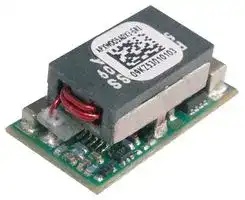
APXW005A0X3-SRZ
Non Isolated POL DC/DC Converter, ProLynx, ITE, 3 V, 18 V, 5 A
⚠️ Reference pricing provided. In case of supply shortages, we will connect you with our trusted procurement partners to ensure your project's continuity.
- Manufacturer: OMNION POWER
- Product type: DC / DC Non Isolated Board Mount Converters - Adjustable Output
- Output Power Max:-; Output Voltage Min:3V; Output Voltage Max:18V; Output Current Max:5A; DC / DC Converter Output Type:Adjustable; DC / DC C; Available until stocks are exhausted
- Depth: 11.43mm
- Width: 20.32mm
- Height: 8.5mm
- Product Range: PicoTLynx AP Series
- Output Power Max: -
- Output Current Max: 5A
- Output Voltage Max: 18V
- Output Voltage Min: 3V
- Input Voltage DC Max: 36V
- Input Voltage DC Min: 9V
- DC / DC Converter Type: -
- Power Supply Applications: ITE
- DC / DC Converter Output Type: Adjustable
| Delivery and price | |
|---|---|
| Units per pack | 50 |
| Price | 13.26 € |
| Current stock | 10+ |
| Lead time | 30 days |
Datasheet

## **DATASHEET** ## **9-36V ProLynx[TM] 5A: Non-Isolated DC-DC Power Modules** **9Vdc –36Vdc input; 3Vdc to 18Vdc output; 5A to 2.5A Scaled output current** ## **Description** **==> picture [63 x 8] intentionally omitted <==** **----- Start of picture text -----**<br> RoHS Compliant<br>**----- End of picture text -----**<br> ## **Applications** - Industrial equipment - Distributed power architectures - Intermediate bus voltage applications - Telecommunications equipment The 9-36V ProLynx[TM] series of power modules are non-isolated dc-dc converters that can deliver up to 5A of output current. These modules operate over an extra wide range of input voltage (VIN = 9Vdc – 36Vdc) and provide a precisely regulated output voltage from 3Vdc to 18Vdc, programmable via an external resistor. Two new features added with this family of products are the ability to externally tune the voltage control loop and a variable current limit inversely dependent on output voltage. Other features include remote On/Off, adjustable output voltage, over current and over temperature protection. The Ruggedized version (-D) is capable of operation up to 105°C and withstand high levels of shock and vibration. The Tunable Loop[TM] , allows the user to optimize the dynamic response of the converter to match the load with reduced amount of output capacitance leading to savings on cost and PWB area and AutoLimit enables the module to deliver the max possible output power across the entire voltage range. ## **Features** - Compliant to RoHS Directive 2011/65/EU and amended Directive (EU) 2015/863 - Compliant to REACH Directive (EC) No 1907/2006 - Compatible in a Pb-free or SnPb reflow environment (Z versions) - Compliant to IPC-9592 (September 2008), Category 2, Class II - Extra Wide Input voltage range (9Vdc–36Vdc) - Output voltage programmable from 3Vdc to 18 Vdc via external resistor - Tunable Loop[TM] to optimize dynamic output voltage response - Patent Pending AutoLimit automatic scaling of current limit with output voltage - Output overcurrent protection (non-latching) - Overtemperature protection - Remote On/Off - Remote Sense - Small size: 20.3 mm x 11.4 mm x 8.5 mm (0.8 in x 0.45 in x 0.335 in) - Wide operating temperature range [-40°C to 105°C (Ruggedized: -D), 85°C(Regular)] - ANSI/UL* 62368-1 and CAN/CSA[†] C22.2 No. 62368-1 Recognized, DIN VDE‡ 0868-1/A11:2017 - ISO** 9001 and ISO 14001 certified manufacturing facilities - UL is a registered trademark of Underwriters Laboratories, Inc. - CSA is a registered trademark of Canadian Standards Association. - VDE is a trademark of Verband Deutscher Elektrotechniker e.V. - ** ISO is a registered trademark of the International Organization of Standards Page 1 © 2023 OmniOn Power Inc. All rights reserved. APXW005_DS Rev. 1.11 ## **Technical Specifications** ## **Absolute Maximum Ratings** Stresses in excess of the absolute maximum ratings can cause permanent damage to the device. These are absolute stress ratings only, functional operation of the device is not implied at these or any other conditions in excess of those given in the operations sections of the data sheet. Exposure to absolute maximum ratings for extended periods can adversely affect the device reliability. |**Parameter**|**Device**|**Symbol**|**Min**|**Max**|**Unit**| |---|---|---|---|---|---| |Input Voltage Continuous|All|VIN|-0.3|37|V| |Operating Ambient Temperature<br>(see Thermal Considerations section)|All<br>-D version|TA<br>TA|-40<br>-40|85<br>105|°C<br>°C| |Storage Temperature|All|Tstg|-55|125|°C| ## **Electrical Specifications** Unless otherwise indicated, specifications apply over all operating input voltage, resistive load, and temperature conditions |**Parameter**|**Device**|**Symbol**<br>~~GO~~|**Min**<br>~~GO~~|**Typ**|**Max**|**Unit**| |---|---|---|---|---|---|---| |OperatingInput Voltage<br>~~GO~~|All<br>~~GO~~<br>~~ee~~|VIN<br>~~GO~~<br>~~GO~~<br>~~es~~|9<br>~~GO~~<br>~~GO~~<br>~~es~~|—<br>~~GO~~<br>~~ee~~|36<br>~~GO~~<br>~~ee~~|Vdc<br>~~GO~~| |Maximum Input Current<br>(VIN=9V to 36V,IO=IO,max)<br>~~ee~~|All<br>~~ee~~<br>~~ee~~<br>~~ee~~|IIN,max<br>~~GO~~<br>~~ee~~<br>~~es~~<br>~~ee~~|~~GO~~<br>~~ee~~<br>~~es~~<br>~~ee~~|~~ee~~<br>~~ee~~<br>~~ee~~|5<br>~~ee~~<br>~~ee~~<br>~~ee~~|Adc<br>~~ee~~<br>~~ee~~| |Input No Load Current<br>(VIN= 28V, IO= 0, module enabled)<br> (VIN= 28V,IO= 0,module enabled)<br>~~ee~~|VO,set= 3Vdc<br>VO,set= 18Vdc<br>~~ee~~<br>~~ee~~<br>~~ee~~<br>~~ee es~~|IIN,No load<br>IIN,No load<br>~~es ~~<br>~~ee~~<br>~~ee~~<br>~~es~~|~~es ~~<br>~~ee~~<br>~~ee~~<br>~~es~~|26<br>50<br> ~~ee~~<br>~~ee~~<br>~~ee~~<br>~~ee~~|~~ee~~<br>~~ee~~<br>~~ee~~|mA<br>mA<br>~~ee~~<br>~~ee~~| |Input Stand-by Current<br> (VIN= 28Vdc,module disabled)<br>~~es~~|All<br>~~ee~~<br>~~es~~<br>~~ee es~~|IIN,stand-by<br>~~ee~~<br>~~es~~<br>~~es~~|~~ee ~~<br>~~es~~<br>~~es~~<br>~~GO~~|3<br> ~~ee~~<br>~~es~~<br>~~ee~~<br>~~GO~~|~~ee~~<br>~~es~~<br>~~GO~~|mA<br>~~ee~~<br>~~es~~| |Inrush Transient<br>~~es~~<br>~~GG~~|All<br>~~es~~<br>~~ee es~~<br>~~GG~~<br>~~eee~~|I2t<br>~~es~~<br>~~es ~~<br>~~GG~~<br>~~eee~~|~~es~~<br> ~~es ~~<br>~~GG~~<br>~~GO~~<br>~~eee~~|~~es~~<br> ~~ee~~<br>~~GG~~<br>~~GO~~<br>~~eee~~|0.5<br>~~es~~<br>~~GG~~<br>~~GO~~<br>~~eee~~|A2s<br>~~es~~<br>~~GG~~<br>~~eee~~| |Input Reflected Ripple Current, peak-to-peak<br>(5Hz to 20MHz, 1μH source impedance; VIN=0<br>to 36V,IO= IO max;See Test Configurations)<br>~~rr~~|All<br>~~rr~~<br>~~eee~~|~~rr~~<br>~~eee~~|~~GO~~<br>~~rr~~<br>~~eee~~|~~GO~~<br>~~rr~~<br>~~eee~~|95<br>~~GO~~<br>~~rr~~<br>~~eee~~|mAp-p<br>~~rr~~<br>~~eee~~| |Input Ripple Rejection(120Hz)<br>~~rr~~|All<br>~~rr~~<br>~~eee~~|~~rr~~<br>~~eee~~|-24<br>~~rr~~<br>~~eee~~|-45<br>~~rr~~<br>~~eee~~|-60<br>~~rr~~<br>~~eee~~|dB<br>~~rr~~<br>~~eee~~| |Output Voltage Set-point|All|VO,set|-2.0||+2.0|% VO,set| |---|---|---|---|---|---|---| |Output Voltage<br>(Over all operating input voltage, resistive load,<br>and temperature conditions until end of life)|All|VO, set|-2.5|—|+2.5|% VO, set| |Adjustment Range (elected by an external<br>resistor)(Some output voltages may not be<br>possible depending on the input voltage – see<br>Feature Descriptions Section)<br>Output Regulation<br>Line (VIN=VIN, minto VIN, max)<br>Load (IO=IO, minto IO, max)<br>Temperature(Tref=TA,minto TA,max)|All<br>All<br>All<br>All|VO|3|—<br>—<br>—|18<br>0.4<br>0.4<br>0.4|Vdc<br>% VO, set<br>% VO, set<br>% VO,set| |Remote Sense Range|All||||0.5|Vdc| Page 2 © 2023 OmniOn Power Inc. All rights reserved. APXW005_DS Rev. 1.11 ## **Technical Specifications** (continued) ## **Electrical Specifications** (continued) |**Parameter**|**Device**|**Symbol**|**Min**|**Typ**|**Max**|**Unit**| |---|---|---|---|---|---|---| |Output Ripple and Noise on nominal output<br>(VIN=VIN, nomand IO=IO, minto IO, maxCo = 0.1μF // 10μF<br>ceramic capacitors)<br>Vout=3.3V, Vin=28V<br>Peak-to-Peak (5Hz to 20MHz bandwidth)<br>RMS (5Hz to 20MHz bandwidth)<br>Vout=18V, Vin=28V<br>Peak-to-Peak (5Hz to 20MHz bandwidth)<br>RMS(5Hz to 20MHz bandwidth)|All<br>All<br>All<br>All|||45<br>14<br>143<br>47||mVpk-pk<br>mVrms<br>mVpk-pk<br>mVrms| |External Capacitance1<br>Without the Tunable LoopTM<br>ESR ≥ 1 mΩ<br>ESR ≥ 10 mΩ<br>With the Tunable LoopTM<br>ESR ≥ 0.15 mΩ<br>ESR ≥ 10 mΩ|All<br>All<br>All<br>All|CO,max<br>CO,max<br>CO,max<br>CO,max|0<br>0<br>0<br>0|—<br>—<br>—<br>—|47<br>100<br>100<br>2000*|μF<br>μF<br>μF<br>μF| |Output Current (Vo=3V)<br>Vo=5V<br>Vo=12V<br>Vo=18V<br>~~po~~|All<br>All<br>All<br>All<br>~~po~~|Io<br>Io<br>Io<br>Io<br>~~po~~|0<br>0<br>0<br>0<br>~~po~~|~~po~~|5<br>4.7<br>3.5<br>2.5<br>~~po~~|Adc<br>Adc<br>Adc<br>Adc<br>~~po~~| |Output Current Limit Inception(HiccupMode)<br>~~po~~|All<br>~~po~~|IO,lim<br>~~po~~|~~po~~|160<br>~~po~~|~~po~~|% Io,max<br>~~po~~| |Output Short-Circuit Current 12Vin 25C<br>(VO≤250mV) (HiccupMode)28Vin<br>~~ee~~|All<br>~~ee~~|IO, s/c<br>~~ee~~|~~ee~~|2<br>~~ee~~|~~ee~~|Adc<br>~~ee~~| |Efficiency (IO=IO, max ,VO= VO,set)<br>VIN= 12Vdc, TA=25°C<br>VIN= 12Vdc, TA=25°C<br>VIN= 28Vdc, TA=25°C<br>VIN= 28Vdc,TA=25°C<br>~~pf~~|VO,set= 3.3Vdc<br>VO,set= 5Vdc<br>VO,set= 12Vdc<br>VO,set= 18Vdc<br>~~pf~~|η<br>η<br>η<br>η<br>~~pf~~|~~pf~~|91.0<br>93.3<br>94.7<br>95.9<br>~~pf~~|~~pf~~|%<br>%<br>%<br>%<br>~~pf~~| |SwitchingFrequency<br>~~pf~~|All<br>~~pf~~|fsw<br>~~pf~~|—<br>~~pf~~|300<br>~~pf~~|—<br>~~pf~~|kHz<br>~~pf~~| ## **General Specifications** |**Parameter**|**Min**|**Typ**|**Max**|**Unit**| |---|---|---|---|---| |Calculated MTBF (IO=0.8IO, max, TA=40°C) Telcordia Issue 2,<br>Method 1,Case 3||17,822,788||Hours| |Weight|—|3.49(0.123)|—|g(oz.)| ## **Feature Specifications** Unless otherwise indicated, specifications apply over all operating input voltage, resistive load, and temperature conditions. See Feature Descriptions for additional information. |**Parameter**|**Device**|**Symbol**|**Min**|**Typ**|**Max**|**Unit**| |---|---|---|---|---|---|---| |On/Off Signal Interface<br>(VIN=VIN, minto VIN, max; open collector or equivalent,<br>Signal referenced to GND)<br>Device is with suffix “4”– Positive Logic (See Ordering Information)<br>Logic High (Module ON)<br>Input High Current<br>Input High Voltage<br>Logic Low (Module OFF)<br>Input Low Current<br>Input Low Voltage|All<br>All<br>All<br>All|IIH<br>VIH<br>IIL<br>VIL|4.2<br>—<br>-0.3|—<br>—<br>—<br>—|160<br>12<br>0.5<br>3.3|µA<br>V<br>mA<br>V| Page 3 © 2023 OmniOn Power Inc. All rights reserved. APXW005_DS Rev. 1.11 ## **Technical Specifications** (continued) ## **Feature Specifications** (continued) |**Parameter**|**Device**|**Symbol**|**Min**|**Typ**|**Max**|**Unit**| |---|---|---|---|---|---|---| |Device Code with no suffix – Negative Logic (See Ordering<br>Information)<br>Logic High (Module OFF)<br>Input High Current<br>Input High Voltage<br>Logic Low (Module ON)<br>Input low Current<br>Input Low Voltage|All<br>All<br>All<br>All|IIH<br>VIH<br>IIL<br>VIL|—<br>1.5<br>—<br>-0.2|—<br>—<br>—<br>—|3<br>36<br>220<br>1|mA<br>Vdc<br>μA<br>Vdc| |Turn-On Delayand Rise Times||||||| |(VIN=VIN, nom, IO=IO, max ,VOto within ±1% of steady state)<br>Case 1:On/Off input is enabled and then input power is<br>applied (delay from instant at which VIN= VIN, minuntil<br>Vo = 10% of Vo, set)<br>Case 2: Input power is applied for at least one second and<br>then the On/Off input is enabled (delay from instant<br>at which Von/Off is enabled until Vo = 10% of Vo, set)<br>Output voltage Rise time (time for Vo to rise from 10% of<br>Vo,set to 90% of Vo,set)|All<br>then the On/Off input is enabled (delay from instant<br>at which Von/Off is enabled until Vo = 10% of Vo, set)<br>All<br>All|Tdelay<br>Tdelay<br>Trise|—<br>—<br>—|9<br>7<br>8|—<br>—<br>—|msec<br>msec<br>msec| |Output voltage overshoot (TA= 25°C<br>VIN= VIN, minto VIN, max,IO= IO, minto IO, max)<br>With or without maximum external capacitance|||||3|%VO, set| |Over Temperature Protection (See Thermal Considerations<br>section)|All|Tref||130||°C| |Input Undervoltage Lockout<br>Turn-on Threshold<br>Turn-off Threshold<br>Hysteresis|All<br>All<br>All|||0.15|7.5<br>7.35|Vdc<br>Vdc<br>Vdc| Page 4 © 2023 OmniOn Power Inc. All rights reserved. APXW005_DS Rev. 1.11 ## **Technical Specifications** (continued) ## **Characteristic Curves** The following figures provide typical characteristics for the 9-36V ProTLynx[TM] 5A at 3.3Vo and at 25°C. **==> picture [8 x 63] intentionally omitted <==** **----- Start of picture text -----**<br> η (%)<br>EFFCIENCY,<br>**----- End of picture text -----**<br> **==> picture [95 x 7] intentionally omitted <==** **----- Start of picture text -----**<br> OUTPUT CURRENT, IO (A)<br>**----- End of picture text -----**<br> **Figure 1. Converter Efficiency versus Output Current.** **==> picture [162 x 123] intentionally omitted <==** **----- Start of picture text -----**<br> aoe) Jatoba tight agit lata<br>TIME, t (1ms/div)<br> (V) (40mV/div)<br>O<br>OUTPUT VOLTAGE V<br>**----- End of picture text -----**<br> **Figure 3. Typical output ripple and noise (VIN = 28V, Io = Io,max).** **==> picture [164 x 159] intentionally omitted <==** **----- Start of picture text -----**<br> TIME, t (5ms/div)<br> (V) (5V/div)<br>ON/OFF<br>ON/OFF VOLTAGE V<br> (V) (1V/div)<br>O<br>V<br>OUTPUT VOLTAGE<br>**----- End of picture text -----**<br> **Figure 5. Typical Start-up Using On/Off Voltage (Io = Io,max).** **==> picture [258 x 359] intentionally omitted <==** **----- Start of picture text -----**<br> 5<br>4 = p\s<br>Ruggedized (D) |Pat (102°C) NWN<br>12Vin 28Vin<br>3 — O.65mis (10 0LF 3<br>Imig1.5m/s (200LFM(300LFM3} NN<br>Zmfs(400LFi}<br>2<br>65 75 35 95 105<br>AMBIENT TEMPERATURE, TA °C<br>Figure 2. Derating Output Current versus Ambient Temperature<br>and Airflow.<br>be eee eee eee ee ee +44<br>TIME, t (20ms /div)<br>Figure 4. Transient Response to Dynamic Load Change from 50%<br>to 100% at 28Vin, Cext - 10uF ceramic + 330uF polymer,<br>CTune=10nF & RTune=150Ω<br> (A)<br>O<br>OUTPUT CURRENT, I<br> (V) (20mV/div)<br>O<br>V<br> (A) (2Adiv)<br>IO<br>OUTPUT CURRENT OUTPUT VOLTAGE<br>**----- End of picture text -----**<br> **Figure 2. Derating Output Current versus Ambient Temperature and Airflow.** **==> picture [165 x 151] intentionally omitted <==** **----- Start of picture text -----**<br> TIME, t (5ms/div)<br> (V) (20V/div)<br>IN<br>INPUT VOLTAGE V<br> (V) (1V/div)<br>O<br>V<br>OUTPUT VOLTAGE<br>**----- End of picture text -----**<br> **Figure 6. Typical Start-up Using Input Voltage (VIN = 28V, Io = Io,max).** Page 5 © 2023 OmniOn Power Inc. All rights reserved. APXW005_DS Rev. 1.11 ## **Technical Specifications** (continued) ## **Characteristic Curves** (continued) The following figures provide typical characteristics for the 9-36V ProLynx[TM] 5A at 5Vo and at 25°C. (4.5A rated output) **==> picture [191 x 319] intentionally omitted <==** **----- Start of picture text -----**<br> AZ<br>Vin=9V Vin=12V_ | Vin=28V<br>80 1=Fa<br>|<br>1<br>yl<br>70i+<br>0 4 2 3<br>OUTPUT CURRENT, IO (A)<br>bod totale pee per pyt<br>TIME, t (1ms/div)<br>η (%)<br>EFFCIENCY,<br> (V) (40mV/div)<br>O<br>V<br>OUTPUT VOLTAGE<br>**----- End of picture text -----**<br> **Figure 7. Converter Efficiency versus Output Current.** **Figure 9. Typical output ripple and noise (VIN = 28V, Io = Io = Io,max ).** **==> picture [184 x 129] intentionally omitted <==** **----- Start of picture text -----**<br> Standard SON<br>= NS<br>12Vin 28Vin<br>eeeRuggedized (D) Part| NC (105°C)<br>,= 0.5mis(1 OOLF Mt}<br>1 mis (200LE MY<br>1.4mis (300LFM)<br>2 sa<br>65 75 65 95<br>AMBIENT TEMPERATURE, TA °C<br> (A)<br>O<br>OUTPUT CURRENT, I<br>**----- End of picture text -----**<br> **Figure 8. Derating Output Current versus Ambient Temperature and Airflow.** **==> picture [240 x 183] intentionally omitted <==** **----- Start of picture text -----**<br> pee [bp][ eae] Pere e abate taper eet rere Perea toret<br>TIME, t (20ms /div)<br>Figure 10. Transient Response to Dynamic Load Change from<br>50% to 100% at 28Vin, Cext - 10uF ceramic + 330uF polymer,<br>CTune=10nF & RTune=150Ω<br> (V) (20mV/div)<br>O<br>V<br> (A) (2Adiv)<br>IO<br>OUTPUT CURRENT OUTPUT VOLTAGE<br>**----- End of picture text -----**<br> **==> picture [168 x 159] intentionally omitted <==** **----- Start of picture text -----**<br> TIME, t (5ms/div)<br> (V) (5V/div)<br>ON/OFF<br>V<br>ON/OFF VOLTAGE<br> (V) (2V/div)<br>O<br>V<br>OUTPUT VOLAGE<br>**----- End of picture text -----**<br> **Figure 11. Typical Start-up Using On/Off Voltage (Io = Io,max).** **==> picture [164 x 155] intentionally omitted <==** **----- Start of picture text -----**<br> TIME, t (5ms/div)<br> (V) (20V/div)<br>IN<br>V<br>INPUT VOLTAGE<br> (V) (2V/div)<br>O<br>V<br>OUTPUT VOLTAGE<br>**----- End of picture text -----**<br> **Figure 12. Typical Start-up Using Input Voltage (VIN = 28V, Io = Io,max** Page 6 © 2023 OmniOn Power Inc. All rights reserved. APXW005_DS Rev. 1.11 ## **Technical Specifications** (continued) ## **Characteristic Curves** (continued) The following figures provide typical characteristics for the 9-36V ProLynx[TM] 5A at 12Vo and at 25°C. (3.5A rated output) **==> picture [169 x 115] intentionally omitted <==** **----- Start of picture text -----**<br> 85 ALAAF : sect<br>80 Mee[|<br>75 df | | | |<br>70 Tete | | |<br>0 05 1 15 2 25<br>OUTPUT CURRENT, IO (A)<br>η (%)<br>EFFCIENCY,<br>**----- End of picture text -----**<br> **Figure 13. Converter Efficiency versus Output Current.** **==> picture [173 x 316] intentionally omitted <==** **----- Start of picture text -----**<br> TIME, t (1ms/div)<br>Figure 15. Typical output ripple and noise (VIN= 28V, Io = Io,max).<br>TIME, t (5ms/div)<br> (V) (40mV/div)<br>O<br>OUTPUT VOLTAGE V<br> (V) (5V/div)<br>ON/OFF<br>ON/OFF VOLTAGE V<br> (V) (5V/div)<br>O<br>V<br>OUTPUT VOLAGE<br>**----- End of picture text -----**<br> **Figure 15. Typical output ripple and noise (VIN= 28V, Io = Io,max).** **Figure 17. Typical Start-up Using On/Off Voltage (Io = Io, max).** **==> picture [168 x 527] intentionally omitted <==** **----- Start of picture text -----**<br> —<br>art (85"<br>2 Ruggedizedi(D] PartNC (105°C)<br>isO.Srvs1.5r's0(00LF(O 0 LF M4<br>| area.Mi<br>65 75 85<br>AMBIENT TEMPERATURE, TAA °C<br>and Airflow.<br>TIME, t (20ms /div)<br>RTune=150Ω<br>TIME, t (5ms/div)<br> (A)<br>O<br>OUTPUT CURRENT, I<br>(V) (100mV/div)<br> (A) (2Adiv)<br>IOO<br> (V) (20V/div)<br>IN<br>V<br> (V) (5V/div)<br>O<br>OUTPUT VOLTAGE INPUT VOLTAGE V<br>**----- End of picture text -----**<br> **AMBIENT TEMPERATURE, TAA °C** **Figure 14. Derating Output Current versus Ambient Temperature and Airflow.** **==> picture [249 x 190] intentionally omitted <==** **----- Start of picture text -----**<br> TIME, t (20ms /div)<br>Figure 16. Transient Response to Dynamic Load Change from<br>50% to 100% at 28Vin, Cext - 3x10uF ceramic CTune=470pF &<br>RTune=150Ω<br>(V) (100mV/div)<br> (A) (2Adiv)<br>IOO<br>OUTPUT CURRENT, OUTPUT VOLTAGE<br>**----- End of picture text -----**<br> **Figure 18. Typical Start-up Using Input Voltage (VIN = 28V, Io = Io, max).** Page 7 © 2023 OmniOn Power Inc. All rights reserved. APXW005_DS Rev. 1.11 ## **Technical Specifications** (continued) ## **Characteristic Curves** (continued) The following figures provide typical characteristics for the 9-36V ProLynx[TM] 5A at 18Vo and at 25°C. (2.5A rated output) **==> picture [225 x 125] intentionally omitted <==** **----- Start of picture text -----**<br> a5 Sa.<br>Ap<br>80 [|<br>75<br>7a<br>Oo o4 1 14 2 25<br>OUTPUT CURRENT, IO (A)<br>Figure 19. Converter Efficiency versus Output Current.<br>η (%)<br>EFFCIENCY,<br>**----- End of picture text -----**<br> **==> picture [167 x 121] intentionally omitted <==** **----- Start of picture text -----**<br> : : " : : t<br>TIME, t (1ms/div)<br> (V) (40mV/div)<br>O<br>OUTPUT VOLTAGE V<br>**----- End of picture text -----**<br> **Figure 21. Typical output ripple and noise (VIN = 28V, Io = Io,max).** **==> picture [187 x 134] intentionally omitted <==** **----- Start of picture text -----**<br> a<br>4 ?8Vin NcO.Smis4 OOLF MM)<br>1.5mi's (300LF M1}<br>0<br>65 75 65 95<br>AMBIENT TEMPERATURE, TA °C<br> (A)<br>O<br>OUTPUT CURRENT, I<br>**----- End of picture text -----**<br> **Figure 20. Derating Output Current versus Ambient Temperature and Airflow.** **==> picture [167 x 164] intentionally omitted <==** **----- Start of picture text -----**<br> fi Hi<br>HHA»<br>ee<br>TIME, t (20ms /div)<br> (V) (200mV/div)<br>O<br>OUTPUT VOLTAGE V<br> (A) (2Adiv)<br>IO<br>OUTPUT CURRENT<br>**----- End of picture text -----**<br> **Figure 22. Transient Response to Dynamic Load Change from 50% to 100% at 28Vin, Cext - 1x10uF ceramic, CTune=150pF & RTune=220Ω** **==> picture [168 x 160] intentionally omitted <==** **----- Start of picture text -----**<br> TIME, t (5ms/div)<br> (V) (5V/div)<br>ON/OFF<br>ON/OFF VOLTAGE V<br> (V) (5V/div)<br>O<br>V<br>OUTPUT VOLTAGE<br>**----- End of picture text -----**<br> **Figure 23. Typical Start-up Using On/Off Voltage (Io = Io,max).** **==> picture [164 x 148] intentionally omitted <==** **----- Start of picture text -----**<br> TIME, t (5ms/div)<br> (V) (20V/div)<br>IN<br>V<br>INPUT VOLTAGE<br> (V) (5V/div)<br>O<br>V<br>OUTPUT VOLTAGE<br>**----- End of picture text -----**<br> **Figure 24. Typical Start-up Using Input Voltage (VIN = 28V, Io = Io,max).** Page 8 © 2023 OmniOn Power Inc. All rights reserved. APXW005_DS Rev. 1.11 ## **Technical Specifications** (continued) ## **Test Configurations** **==> picture [202 x 312] intentionally omitted <==** **----- Start of picture text -----**<br> TO OSCILLOSCOPE CURRENT PROBE<br>Rw LTEST<br>VIN(+)<br>1μH<br>CS 1000μF CIN<br>Electrolytic<br>2x100μF<br>E.S.R.<0.1 Tantalum<br>@ 20°C 100kHz<br>COM<br>NOTE: Measure input reflected ripple current with a simulated<br>source inductance (LTEST) of 1μH. Capacitor CS offsets<br>possible battery impedance. Measure current as shown<br>above.<br>Figure 25. Input Reflected Ripple Current Test Setup.<br>COPPER STRIP<br>Vo+ — RESISTIVELOAD<br>0.1uF 10uF<br>COM<br>SCOPE USING<br>ao e<br>a GROUND PLANEBNC SOCKET<br>NOTE: All voltage measurements to be taken at the module<br>terminals, as shown above. If sockets are used then<br>Kelvin connections are required at the module terminals<br>to avoid measurement errors due to socket contact<br>resistance.<br>BATTERY<br>**----- End of picture text -----**<br> **Figure 25. Input Reflected Ripple Current Test Setup.** **Figure 26. Output Ripple and Noise Test Setup.** **==> picture [168 x 128] intentionally omitted <==** **----- Start of picture text -----**<br> Rdistribution Rcontact Rcontact Rdistribution<br>VIN(+) VO<br>VIN VO RLOAD<br>Rdistribution Rcontact Rcontact Rdistribution<br>COM COM<br>NOTE: All voltage measurements to be taken at the module<br>terminals, as shown above. If sockets are used then<br>Kelvin connections are required at the module terminals<br>to avoid measurement errors due to socket contact<br>resistance.<br>**----- End of picture text -----**<br> **Figure 27. Output Voltage and Efficiency Test Setup.** **==> picture [150 x 23] intentionally omitted <==** **----- Start of picture text -----**<br> VO. IO<br>Efficiency = VIN. IIN x 100 %<br>**----- End of picture text -----**<br> ## **Design Considerations** ## **Input Filtering** The 9-36V ProLynx[TM] module should be connected to a low ac-impedance source. A highly inductive source can affect the stability of the module. An input capacitance must be placed directly adjacent to the input pin of the module, to minimize input ripple voltage and ensure module stability. To minimize input voltage ripple, ceramic capacitors are recommended at the input of the module. Figure 28 shows the input ripple voltage for various output voltages at maximum load current with 2x10 µF or 3x10 µF ceramic capacitors and an input of 12V, while Fig. 29 shows the input ripple for an input voltage of 28V. **==> picture [162 x 156] intentionally omitted <==** **----- Start of picture text -----**<br> es en ee<br>|<br>os | | |}<br>6 a<br>os ff ae<br>Output Voltage (Vdc)<br>Of lem<br>Input Ripple Voltage (mV p-p)<br>**----- End of picture text -----**<br> **Figure 28. Input ripple voltage for various output voltages with 2x10 µF or 3x10 µF ceramic capacitors at the input (maximum load). Input voltage is 12V.** **==> picture [165 x 135] intentionally omitted <==** **----- Start of picture text -----**<br> LL IZLE<br>os i =<br>iswot 41 LT |<br>. Z| emer<br>MT [eso<br>3 5 7 9 11 13<br>Output Voltage (Vdc)<br>Input Ripple Voltage (mV p-p)<br>**----- End of picture text -----**<br> **Figure 29. Input ripple voltage for various output voltages with 2x10 µF or 3x10 µF ceramic capacitors at the input (maximum load). Input voltage is 28V.** ## **Output Filtering** The 9-36V ProLynx[TM] modules are designed for low output ripple voltage and will meet the maximum output ripple specification with 0.1 µF ceramic and 10 µF ceramic capacitors at the output of the module. However, additional output filtering may be required by the system designer for a number of reasons. First, there may be a need to further reduce the output ripple and noise of the module. Second, the dynamic response characteristics may need to be customized to a particular load step change. Page 9 © 2023 OmniOn Power Inc. All rights reserved. APXW005_DS Rev. 1.11 ## **Technical Specifications** (continued) To reduce the output ripple and improve the dynamic response to a step load change, additional capacitance at the output can be used. Low ESR polymer and ceramic capacitors are recommended to improve the dynamic response of the module. Figures 30 and 31 provide output ripple information for different external capacitance values at various Vo and for full load currents. For stable operation of the module, limit the capacitance to less than the maximum output capacitance as specified in the electrical specification table. Optimal performance of the module can be achieved by using the Tunable Loop[TM] feature described later in this data sheet. ## **Safety Considerations** For safety agency approval the power module must be installed in compliance with the spacing and separation requirements of the end-use safety agency standards, i.e., UL ANSI/UL 62368-1 and CAN/CSA C22.2 No. 62368-1 Recognized, DIN VDE 0868-1/A11:2017 (EN62368-1:2014/A11:2017) For the converter output to be considered meeting the requirements of safety extra-low voltage (SELV) or ES1, the input must meet SELV/ES1 requirements. The power module has extra-low voltage (ELV) outputs when all inputs are ELV. The input to these units is to be provided with a fastacting fuse with a maximum rating of 8A in the positive input lead. ## **Feature Descriptions** ## **Remote Enable** **Figure 30. Output ripple voltage for various output voltages with external 1x10 µF, 2x10 µF or 4x10 µF ceramic capacitors at the output (max. load). Input voltage is 12V.** **Figure 31. Output ripple voltage for various output voltages with external 1x10 µF, 2x10 µF or 4x10 µF ceramic capacitors at the output (max. load). Input voltage is 28V.** The 9-36V ProLynx[TM] modules feature an On/Off pin for remote On/Off operation. Two On/Off logic options are available. In the Positive Logic On/Off option, (device code suffix “4” – see Ordering Information), the module turns ON during a logic High on the On/Off pin and turns OFF during a logic Low. With the Negative Logic On/Off option, (no device code suffix, see Ordering Information), the module turns OFF during logic High and ON during logic Low. The On/Off signal is always referenced to ground. For positive logic modules, the circuit configuration for using the On/Off pin is shown in Figure 32. When the external transistor Q1 is in the OFF state, the ON/OFF pin is pulled high and transistor Q2 is OFF leading to Q3 also being OFF which turns the module ON. The external resistor Rpullup (100k recommended) must be sized so that VON/OFF is never more than 12V when Q1 is OFF. In particular, if Vpullup is made the same as the input voltage Vin, the resistor Rpullup must be large enough so that VON/OFF is never more than 12V. If the On/ Off pin is left floating the module will be in the ON state. For negative logic On/Off modules, the circuit configuration is shown in Fig. 33. When the external transistor Q1 is in the ON state, the ON/OFF pin is pulled low causing transistor Q2 to be OFF and the module to be turned ON. To turn the module OFF, Q1 is turned OFF, causing the ON/OFF pin to be pulled high turning Q2 ON and the module to be turned OFF. If the On/Off pin is left floating, the module will be in the OFF state. Page 10 © 2023 OmniOn Power Inc. All rights reserved. APXW005_DS Rev. 1.11 ## **Technical Specifications** (continued) **Figure 32. Circuit configuration for using positive On/Off logic.** **Figure 34. Graph showing maximum output current capability at different output voltages.** ## **Over Temperature Protection** To provide protection in a fault condition, the unit is equipped with a thermal shutdown circuit. The unit will shutdown if the overtemperature threshold of 130°C is exceeded at the thermal reference point Tref. The thermal shutdown is not intended as a guarantee that the unit will survive temperatures beyond its rating. Once the unit goes into thermal shutdown it will then wait to cool before attempting to restart. ## **Input Undervoltage Lockout** **Figure 33. Circuit configuration for using negative On/Off logic.** ## **Overcurrent Protection** To provide protection in a fault (output overload) condition, the unit is equipped with internal currentlimiting circuitry and can endure current limiting continuously. At the point of current-limit inception, the unit enters hiccup mode. The unit operates normally once the output current is brought back into its specified range. The 9-36V ProLynx modules employ an innovative, patent pending, ‘AutoLimit’ capability. This results in automatic scaling of current limit with output voltage through an inverse relationship of the current limit threshold with the output voltage. This feature shown graphically in Fig. 34, allows higher output currents to be drawn from the module at lower output voltages thereby optimizing the power delivery capability of the module. At input voltages below the input undervoltage lockout limit, the module operation is disabled. The module will begin to operate at an input voltage above the undervoltage lockout turn-on threshold. ## **Output Voltage Programming** The output voltage of the 9-36V ProLynx[TM] module can be programmed to any voltage from 3Vdc to 18Vdc by connecting a resistor between the Trim and GND pins of the module. Certain restrictions apply on the output voltage set point depending on the input voltage. These are shown in the Output Voltage vs. Input Voltage Set Point Area plot in Fig. 35. Without an external resistor between Trim and GND pins, the output of the module will be 0.7Vdc. To calculate the value of the trim resistor, Rtrim for a desired output voltage, use the following equation **:** **==> picture [113 x 33] intentionally omitted <==** Rtrim is the external resistor in k Ω, and Vo is the desired output voltage. Page 11 © 2023 OmniOn Power Inc. All rights reserved. APXW005_DS Rev. 1.11 ## **Technical Specifications** (continued) ## **Voltage Margining** Output voltage margining can be implemented in the 9-36V ProLynx[TM] modules by connecting a resistor, Rmargin-up, from the Trim pin to the ground pin for margining-up the output voltage and by connecting a resistor, Rmargin-down, from the Trim pin to output pin for margining-down. Figure 37 shows the circuit **Figure 35. Output Voltage vs. Input Voltage Set Point Area plot showing limits where the output voltage can be set for different input voltages** configuration for output voltage margining. The POL Programming Tool, available at **omnionpower.com** ~~—~~ under the Design Tools section, also calculates the values of Rmargin-up and Rmargin-down for a specific output voltage and % margin Please consult your local OmniOn technical representative for additional details. Table 1 provides Rtrim values required for some common output voltages. **Table 1** |**VO, set (V)**|**Rtrim (KΩ)**| |---|---| |3.3|26.92| |5|16.27| |6|13.20| |9|8.43| |12|6.19| |15|4.89| |18|4.04| By using a ±0.5% tolerance trim resistor with a TC of ±100ppm, a set point tolerance of ±1.5% can be achieved as specified in the electrical specification. Remote Sense The 9-36V ProLynx[TM] power modules have a Remote Sense feature to minimize the effects of distribution losses by regulating the voltage between the VS+ and Vo pin. The voltage between the VS+ pin and Vo pin should not exceed 0.5V. **==> picture [192 x 89] intentionally omitted <==** **----- Start of picture text -----**<br> VIN(+) VO(+)<br>VS+<br>ON/OFF<br>TRIM LOAD<br>Rtrim<br>GND<br>**----- End of picture text -----**<br> **Figure 36. Circuit configuration for programming output voltage using an external resistor** **Figure 37. Circuit Configuration for margining Output voltage** ## **Tunable Loop[TM ]** The 9-36V ProLynx[TM] modules have a new feature that optimizes transient response of the module called Tunable Loop[TM] . External capacitors are usually added to the output of the module for two reasons: to reduce output ripple and noise (see Figs 30 and 31) and to reduce output voltage deviations from the steady-state value in the presence of dynamic load current changes. Adding external capacitance however affects the voltage control loop of the module, typically causing the loop to slow down with sluggish response. Larger values of external capacitance could also cause the module to become unstable. The Tunable Loop[TM] allows the user to externally adjust the voltage control loop to match the filter network connected to the output of the module. The Tunable Loop[TM] is implemented by connecting a series R-C between the VS+ and TRIM pins of the module, as shown in Fig. 38. This R-C allows the user to externally adjust the voltage loop feedback compensation of the module. Page 12 © 2023 OmniOn Power Inc. All rights reserved. APXW005_DS Rev. 1.11 ## **Technical Specifications** (continued) Recommended values of RTUNE and CTUNE for different output capacitor combinations are given in Tables 2, 3 and 4. Tables 2 and 3 show recommended values of RTUNE and CTUNE for different values of ceramic output capacitors up to 100µF that might be needed for an application to meet output ripple and noise requirements. Selecting RTUNE and CTUNE according to Tables 2 and 3 will ensure stable operation of the module In applications with tight output voltage limits in the presence of dynamic current loading, additional output capacitance will be required.Table 4 lists recommended values of RTUNE and CTUNE in order to meet 2% output voltage deviation limits for some common output voltages in the presence of a 50% of full load step change with an input voltage of 12 or 28V. Table 3. General recommended values of of RTUNE and CTUNE for Vin=28V and various external ceramic capacitor combinations. Vo=5V |**Co**|**1x10µF **|**1x22µF **|**2x22µF **|**4x22µF **|**6x22µF **| |---|---|---|---|---|---| |RTUNE<br>CTUNE|330<br>220pF|220<br>390pF|220<br>680pF|150<br>1000pF|150<br>1800pF| Vo=12V |**Co**|**1x10mF**|**1x10mF**<br>**1x22mF**|**2x22mF**|**4x22mF**|**6x22mF**| |---|---|---|---|---|---| |RTUNE<br>CTUNE|330<br>120pF|330<br>470pF|270<br>1000pF|270<br>1800pF|180<br>2700pF| Table 4. Recommended values of RTUNE and CTUNE to obtain transient deviation of 2% of Vout for a 50% of full load step. |**Vin**|**12V**|**12V**|**28V**|**28V**|**28V**|**28V**| |---|---|---|---|---|---|---| |**Vo**|**3.3V**|**5V**|**3.3V**|**5V**|**12V**|**18V**| |**ΔI **|**2.5A**|**2.35A**|**2.5A**|**2.35A**|**1.75A**|**1.5A**| |Co|1x330µF<br>OsCon|1x330µF<br>OsCon|1x330µF<br>1x330µF<br>OsCon|1x330µF<br>1x330µF<br>OsCon|1x330µF<br>2x22µF 1x22µF|2x22µF 1x22µF| |RTUNE|180|180|180|220|270|330| |CTUNE|22nF|22nF|6800pF|6.8nF|470pF 47|F 47pF| |ΔV|39mV|37mV|36mV|34mV 220mV 310mV|34mV 220mV 310mV|34mV 220mV 310mV| **Figure. 38. Circuit diagram showing connection of RTUME and CTUNE to tune the control loop of the module** Please contact your OmniOn technical representative to obtain more details of this feature as well as for guidelines on how to select the right value of external R-C to tune the module for best transient performance and stable operation for other output capacitance values or input voltages other than 12 / 28V. Table 2. General recommended values of of RTUNE and CTUNE for Vin=12V and various external ceramic capacitor combinations. Vo=5V |**Co**|**1x10µF **|**1x22µF **|**2x22uF**|**4x22uF**|**6x22uF**| |---|---|---|---|---|---| |RTUNE<br>**CTUNE**|330<br>680pF|270<br>1200pF|270<br>2700pF|220<br>4700pF|180<br>5600pF| Page 13 © 2023 OmniOn Power Inc. All rights reserved. APXW005_DS Rev. 1.11 ## **Technical Specifications** (continued) ## **Thermal Considerations** Power modules operate in a variety of thermal environments; however, sufficient cooling should always be provided to help ensure reliable operation. Considerations include ambient temperature, airflow, module power dissipation, and the need for increased reliability. A reduction in the operating temperature of the module will result in an increase in reliability. The thermal data presented here is based on physical measurements taken in a wind tunnel. The test set-up is shown in Figure 39. The preferred airflow direction for the module is in Figure 40. The derating data applies to airflow in either direction of the module’s short axis. **==> picture [200 x 202] intentionally omitted <==** **----- Start of picture text -----**<br> 25.4_<br>Wind Tunnel | + (1.0)<br>———~»<br>PWBs<br>Power Module<br>76.2_<br>(3.0)<br>x<br>Probe Location<br>for measuring<br>12.7_ airflow and<br>(0.50) ambient<br>temperature<br>Air<br>flow<br>**----- End of picture text -----**<br> The thermal reference points, Tref used in the specifications are also shown in Figure 40. For reliable operation the temperatures at these points should not exceed 115°C. The output power of the module should not exceed the rated power of the module (Vo,set x Io,max). Please refer to the Application Note “Thermal Characterization Process For Open-Frame BoardMounted Power Modules” for a detailed discussion of thermal aspects including maximum device temperatures. **Figure 40. Preferred airflow direction and location of hot-spot of the module (Tref).** **Fgure 39. Thermal Test Setup.** Page 14 © 2023 OmniOn Power Inc. All rights reserved. APXW005_DS Rev. 1.11 ## **Technical Specifications** (continued) ## **Shock and Vibration** The ruggedized (-D version) of the modules are designed to withstand elevated levels of shock and vibration to be able to operate in harsh environments. The ruggedized modules have been successfully tested to the following conditions: ## **Non operating random vibration:** Random vibration tests conducted at 25°C, 10 to 2000Hz, for 30 minutes each level, starting from 30Grms (Z axis) and up to 50Grms (Z axis). The units were then subjected to two more tests of 50Grms at 30 minutes each for a total of 90 minutes. ## **Operating shock to 40G per Mil Std. 810G, Method 516.4 Procedure I:** The modules were tested in opposing directions along each of three orthogonal axes, with waveform and amplitude of the shock impulse characteristics as follows: All shocks were half sine pulses, 11 milliseconds (ms) in duration in all 3 axes. Units were tested to the Functional Shock Test of MIL-STD-810, Method 516.4, Procedure I - Figure 516.4-4. A shock magnitude of 40G was utilized. The operational units were subjected to three shocks in each direction along three axes for a total of eighteen shocks. ## **Operating vibration per Mil Std 810G, Method 514.5 Procedure I:** The ruggedized (-D version) modules are designed and tested to vibration levels as outlined in MIL-STD-810G, Method 514.5, and Procedure 1, using the Power Spectral Density (PSD) profiles as shown in Table 1 and Table 2 for all axes. Full compliance with performance specifications was required during the performance test. No damage was allowed to the module and full compliance to performance specifications was required when the endurance environment was removed. The module was tested per MIL-STD-810, Method 514.5, Procedure I, for functional (performance) and endurance random vibration using the performance and endurance levels shown in Table 5 and Table 6 for all axes. The performance test has been split, with one half accomplished before the endurance test and one half after the endurance test (in each axis). The duration of the performance test was at least 16 minutes total per axis and at least 120 minutes total per axis for the endurance test. The endurance test period was 2 hours minimum per axis. **Table 5: Performance Vibration Qualification - All Axes** **==> picture [540 x 244] intentionally omitted <==** **----- Start of picture text -----**<br> ||||||||||| |---|---|---|---|---|---|---|---|---|---| |Frequency|(Hz)|PSD Level (G2/Hz)|Frequency|(Hz)|PSD Level (G2/Hz)|Frequency|(Hz)|PSD Level (G2/Hz)| |ae|10|(On|1.14E-03|170|2.54E-03|690|1.03E-03| |30|5.96E-03|230|3.70E-03|800|7.29E-03| |Rs|nD(f(T| |Pf|40|9.53E-04|290|7.99E-04|890|1.00E-03| |PO|50|2.08E-03|340|1.12E-02|1070|2.67E-03| |PO|90|2.08E-03|370|1.12E-02|1240|1.08E-03| |PO|110|7.05E-04|430|8.84E-04|1550|2.54E-03| |130|5.00E-03|490|1.54E-03|1780|2.88E-03| |es|nDnD(OQef| |Pf|140|8.20E-04|560|5.62E-04|2000|5.62E-04| |Table 6: Endurance Vibration Qualification - All Axes| |Frequency|(Hz)|PSD Level (G2/Hz)|Frequency|(Hz)|PSD Level (G2/Hz)|Frequency|(Hz)|PSD Level (G2/Hz)| |a|10|CO|0.00803|170|0.01795|690|0.00727| |30|0.04216|230|0.02616|800|0.05155| |es|PDQO| |40|0.00674|290|0.00565|890|0.00709| |Rs|I| |Rs|50|0.01468|I|340|0.07901|1070|0.01887| |es|90|0.01468|I|OR|370|0.07901|On|1240|0.00764| |110|0.00498|430|0.00625|1550|0.01795| |es|I|(RDQO| |130|0.03536|490|0.01086|1780|0.02035| |Rs| |140|0.0058|560|0.00398|2000|0.00398| |es|I (RD(OQ| **----- End of picture text -----**<br> Page 15 © 2023 OmniOn Power Inc. All rights reserved. APXW005_DS Rev. 1.11 ## **Technical Specifications** (continued) ## **Example Application Circuit** ## **Requirements:** Vin: 28V Vout: 12V Iout: 2.6A max., worst case load transient is from 1.75A to 2.6A DVout: 1.5% of Vout (180mV) for worst case load transient Vin, ripple 1.5% of Vin (420mV, p-p) CI1 1 x 0.01 μ F/50V, 0603 ceramic capacitor CI2 2 x 10 μ F/50V ceramic capacitor (e.g. Murata GRM32ER71H106K) CI3 47 μ F/63V bulk electrolytic CO1 1 x 0.01 μ F/25V, 0306 ceramic capacitor (e.g. Murata LLL185R71E103MA01L)) CO2 2 x 22 μ F/25V ceramic capacitor (e.g. Murata GCM32ER71E106KA42) CO3 NA CTune 470pF ceramic capacitor (can be 1206, 0805 or 0603 size) RTune 150 ohms SMT resistor (can be 1206, 0805 or 0603 size) RTrim 6.19k Ω resistor Page 16 © 2023 OmniOn Power Inc. All rights reserved. APXW005_DS Rev. 1.11 ## **Technical Specifications** (continued) ## **Mechanical Outline** Dimensions are in millimeters and (inches). Tolerances: x.x mm ± 0.5 mm (x.xx in. ± 0.02 in.) [unless otherwise indicated] x.xx mm ± 0.25 mm (x.xxx in ± 0.010 in.) Page 17 © 2023 OmniOn Power Inc. All rights reserved. APXW005_DS Rev. 1.11 ## **Technical Specifications** (continued) ## **Recommended Pad Layout** Dimensions are in millimeters and (inches). Tolerances:x.x mm ± 0.5 mm (x.xx in. ± 0.02 in.) [unless otherwise indicated] x.xx mm ± 0.25 mm (x.xxx in ± 0.010 in.) |**PIN**|**FUNCTION**| |---|---| |1|ON/OFF| |2|VIN| |3|GND| |4|TRIM| |5|VOUT| |6|VS+| Page 18 © 2023 OmniOn Power Inc. All rights reserved. APXW005_DS Rev. 1.11 ## **Technical Specifications** (continued) ## **Packaging Details** The 9-36V ProLynx[TM] modules are supplied in tape & reel as standard. Modules are shipped in quantities of 250 modules per reel. All Dimensions are in millimeters and (in inches). Reel Dimensions: Outside Dimensions: 330.2 mm (13.00) Inside Dimensions: 177.8 mm (7.00”) Tape Width: 44.00 mm (1.732”) Page 19 © 2023 OmniOn Power Inc. All rights reserved. APXW005_DS Rev. 1.11 ## **Technical Specifications** (continued) ## **Surface Mount Information** ## **Pick and Place** The 9-36V ProLynx[TM] modules use an open frame construction and are designed for a fully automated assembly process. The modules are fitted with a label designed to provide a large surface area for pick and place operations. The label meets all the requirements for surface mount processing, as well as safety standards, and is able to withstand reflow temperatures of up to 300°C. The label also carries product information such as product code, serial number and the location of manufacture. ## **Nozzle Recommendations** The module weight has been kept to a minimum by using open frame construction. Variables such as nozzle size, tip style, vacuum pressure and placement speed should be considered to optimize this process. The minimum recommended inside nozzle diameter for reliable operation is 3mm. The maximum nozzle outer diameter, which will safely fit within the allowable component spacing, is 7 mm. For questions regarding Land grid array(LGA) soldering, solder volume; please contact OmniOn for special manufacturing process instructions. ## **MSL Rating** The 9-36V ProLynx[TM] modules have a MSL rating of 2a. ## **Storage and Handling** The recommended storage environment and handling procedures for moisture-sensitive surface mount packages is detailed in J-STD-033 Rev. A (Handling, Packing, Shipping and Use of Moisture/ Reflow Sensitive Surface Mount Devices). Moisture barrier bags (MBB) with desiccant are required for MSL ratings of 2 or greater. These sealed packages should not be broken until time of use. Once the original package is broken, the floor life of the product at conditions of ≤ 30°C and 60% relative humidity varies according to the MSL rating (see J-STD-033A). The shelf life for dry packed SMT packages will be a minimum of 12 months from the bag seal date, when stored at the following conditions: < 40° C, < 90% relative humidity. ## **Bottom Side / First Side Assembly** This module is not recommended for assembly on the bottom side of a customer board. If such an assembly is attempted, components may fall off the module during the second reflow process. ## **Lead Free Soldering** The 9-36V ProLynx[TM] modules are lead-free (Pb-free) and RoHS compliant and fully compatible in a Pb-free soldering process. Failure to observe the instructions below may result in the failure of or cause damage to the modules and can adversely affect long-term reliability. **Figure 41. Recommended linear reflow profile using Sn/Ag/Cu solder.** ## **Pb-free Reflow Profile** Power Systems will comply with J-STD-020 Rev. C (Moisture/Reflow Sensitivity Classification for Nonhermetic Solid State Surface Mount Devices) for both Pb-free solder profiles and MSL classification procedures. This standard provides a recommended forced-air-convection reflow profile based on the volume and thickness of the package (table 4-2). The suggested Pb-free solder paste is Sn/Ag/Cu (SAC). The recommended linear reflow profile using Sn/Ag/Cu solder is shown in Fig. 41. Soldering outside of the recommended profile requires testing to verify results and performance. ## **Post Solder Cleaning and Drying Considerations** Post solder cleaning is usually the final circuit-board assembly process prior to electrical board testing. The result of inadequate cleaning and drying can affect both the reliability of a power module and the testability of the finished circuit-board assembly. For guidance on appropriate soldering, cleaning and drying procedures, refer to Board Mounted Power Modules: Soldering and Cleaning Application Note (AN04-001). Page 20 © 2023 OmniOn Power Inc. All rights reserved. APXW005_DS Rev. 1.11 ## **Technical Specifications** (continued) ## **EMC Considerations** The circuit and plots in Figure 42 shows a suggested configuration to meet the radiated emission limits of EN55032 Class A. Actual performance depends on layout and external components used. CI1 1 x 0.01 μ F/50V, 0603 ceramic capacitor CI2 2 x 10 μ CO1 1 x 0.01 μ CO2 2 x 10 μ RTrim 6.19K Ω resistor 2 x 10 μ F/50V ceramic capacitor (e.g. Murata GRM32ER71H106K) 1 x 0.01 μ F/25V, 0306 ceramic capacitor (e.g. Murata LLL185R71E103MA01L)) 2 x 10 μ F/25V ceramic capacitor (e.g. Murata GCM32ER71E106KA42) EUT: APXW005A0X3-SRZ / TEM Cell **Fig 42 – EMI Plot of APXW005 on evaluation board with 12 V in @ 1.8 A in / 5 Vdc @ 4 A out** Page 21 © 2023 OmniOn Power Inc. All rights reserved. APXW005_DS Rev. 1.11 ## **Technical Specifications** (continued) ## **EMC Considerations** (Continued) **Fig 43 – EMI Plot of APXW005 on evaluation board with 24 V in @ 0.9 A in / 5 Vdc @ 4 A out** Page 22 © 2023 OmniOn Power Inc. All rights reserved. APXW005_DS Rev. 1.11 ## **Technical Specifications** (continued) ## **Ordering Information** Please contact your OmniOn Sales Representative for pricing, availability and optional features. **Table 8. Device Codes** |**Device Code**|**Input**<br>**Voltage Range **|**Output**<br>**Voltage **|**Output**<br>**Current**|**On/Off**<br>**Logic**|**Connector**<br>**Type **|**Ordering Code**| |---|---|---|---|---|---|---| |APXW005A0X3-SRZ|9 – 36Vdc<br>APXW005A0X43-SRZ<br>APXW005A0X3-SRDZ|3 – 18Vdc|5A – 2.5A|Negative|SMT|CC109151916| |APXW005A0X43-SRZ||||Positive|SMT|CC109151908| |APXW005A0X3-SRDZ||||Negative|SMT|CC109168852| - -Z refers to RoHS compliant parts **Table 9. Coding Scheme** |**TLynx**<br>**family**|**Sequencing**<br>**feature.**|**Sequencing**<br>**Input**<br>**voltage**<br>**range **|**Output**<br>**current**|**Output**<br>**current**<br>**Output**<br>**voltage**|**On/Off**<br>**logic**|**Remote**<br>**Sense**|**Options**|**Options**|**ROHS**<br>**Compliance**| |---|---|---|---|---|---|---|---|---|---| |AP|X|W|005|X|4|3|-SR|-D|Z| ||X = w/o Seq.|W =<br>9-36V|W =<br>5A|X =<br>programmabl<br>e output|4 =<br>positive<br>No entry =<br>negative|No entry =<br>Availabl<br>e|S = Surface<br>Mount<br>R = Tape &<br>Reel|D = 105°C<br>operating<br>ambient, 40G<br>operating<br>shock as per<br>MIL Std 810G|Z = ROHS| Page 23 © 2023 OmniOn Power Inc. All rights reserved. APXW005_DS Rev. 1.11 ## **Change History (excludes grammar & clarifications)** |**Revision**|**Date**|**Description of the change**| |---|---|---| |1.10|06/23/2022|Updated Cap notation typo| |1.11|12/13/2023|Updated as per OmniOn template| Page 24 © 2023 OmniOn Power Inc. All rights reserved. APXW005_DS Rev. 1.11 ## **OmniOn Power Inc.** 601 Shiloh Rd. Plano, TX USA ## **omnionpower.com** We reserve the right to make technical changes or modify the contents of this document without prior notice. OmniOn Power does not accept any responsibility for errors or lack of information in this document and makes no warranty with respect to and assumes no liability as a result of any use of information in this document. We reserve all rights in this document and in the subject matter and illustrations contained therein. Any reproduction, disclosure to third parties or utilization of its contents – in whole or in parts – is forbidden without prior written consent of OmniOn Power. This document does not convey license to any patent or any intellectual property right. Copyright© 2023 OmniOn Power Inc. All rights reserved. Page 25 © 2023 OmniOn Power Inc. All rights reserved. APXW005_DS Rev. 1.11
Updated at June 5, 2026
About Novapart
Novapart is a B2B electronic component broker specialising in stock shortages and cost reduction. We source hard-to-find parts and identify compliant alternatives across a catalogue of 410,000+ components from 500+ manufacturers.
Learn more →Stock Shortage Specialist
When a component is unavailable, discontinued or has an unacceptable lead time, we tap into our network of vetted European and Asian distributors to source what you need — without compromising on quality or traceability.
Request a quote →Compliant Alternatives
We identify pin-to-pin, electrically equivalent substitutes that meet the same certifications (RoHS, AEC-Q100, REACH) as your original specification — validated against datasheets, not just part numbers. Often at a lower cost.
BOM Analysis service →