
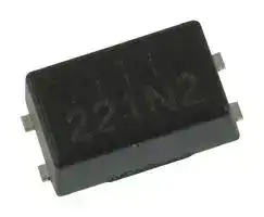


APV2111VY
MOSFET Relay, SPST-NO (1 Form A), SSOP-4, Surface Mount
- Manufacturer: PANASONIC
- Product type: MOSFET Solid State Relays
- SVHC: To Be Advised
- Load Type: -
- Contact Form: SPST-NO (1 Form A)
- Load Current: -
- Product Range: APV Series
- Relay Mounting: Surface Mount
- Relay Terminals: Gull Wing
- Load Voltage Max: -
- Isolation Voltage: 1.5kV
- I/O Capacitance Typ: 0.8pF
- On State Resistance Max: -
- MOSFET Relay Package Style: SSOP-4
- Off State Leakage Current Max: -
| Delivery and price | |
|---|---|
| Units per pack | 100 |
| Price | 0.84 € |
| Current stock | 10+ |
| Lead time | 30 days |
**==> picture [97 x 43] intentionally omitted <==**

## Photovoltaic MOSFET Driver

Product Catalog

**==> picture [503 x 423] intentionally omitted <==**

2022.4

## **Photovoltaic MOSFET Driver**

## **Photovoltaic MOSFET drivers of wide variation**

~~P~~ ~~**FEATURES** o~~ **High-speed switching High insulation** DIP type: 5,000 Vrms, SOP type: 2,500 Vrms, : SSOP type: 1,500 Vrms **Extensive product lineup** Products include SSOP, SOP4-pin and DIP6-pin.

**==> picture [463 x 177] intentionally omitted <==**

**----- Start of picture text -----**<br>
High-speed switching<br>8.8 6.4 High insulation<br>3.9 DIP type: 5,000 Vrms, SOP type: 2,500 Vrms,<br>ha :<br>8.8 6.4 4.3 4.42 2.65 4.451.8 SSOP type: 1,500 Vrms Extensive product lineup<br>3.6<br>Products include SSOP, SOP4-pin and DIP6-pin.<br>Geos :<br>+ + TYPICAL APPLICATIONS<br>1 6 1 4<br>Power supply (Vcc) for electronic circuits<br>2 Driving MOSFET<br>3 ー 4 2 ー 3 Note: Please contact our sales representative for automotive applications of PhotoMOS.<br>FO HO 9<br>(Unit: mm)<br>Control circuit Control circuit<br>**----- End of picture text -----**<br>


## | **TYPES**

|Output rating|Output rating|Package<br>Short circuit|Part No.|Part No.|Part No.|Part No.|Packing quantity|Packing quantity|
|---|---|---|---|---|---|---|---|---|
|Drop-out<br>voltage<br>(Typ.)|Short circuit<br>current<br>(Typ.)||Through hole<br>terminal|Surface mount terminal|||Tube|Tape and reel|
||||Tube packing<br>style|Tube packing<br>style|Tape and reel<br>packingstyle X, Y*1|Tape and reel<br>packingstyle1Y|||
|8.7V|14μA|DIP6-pin|APV1122|APV1122A|APV1122AX|-|1-tube:50pcs.<br>Outer carton:500 pcs.|1-reel:1,000pcs.<br>Outer carton:1,000 pcs.|
|8.7V|14 μA|SOP4-pin*3|-|APV1121S|APV1121SX|-|1-tube:100pcs.<br>Outer carton:2,000pcs.|1-reel:1,000pcs.<br>Outer carton:1,000pcs.|
|8.2V|8 μA||-|APV2121S|APV2121SX|-|||
|8.2V|8μA|SSOP*4|-|-|APV2111VY|APV2111V1Y|-|Packing style Y<br>1-reel:3,500pcs.<br>Outer carton:3,500pcs.<br>Packing style1Y<br>1-reel:1,000pcs.<br>Outer carton:1,000 pcs.|


- *1. 1:DIP type is picked from 1/2/3-pin side, SOP type is picked from 1/2-pin side, SSOP type is picked from 1/4-pin side.

- *2.  For DIP type picked from the 4/6-pin side, for the SOP type picked from the 3/4-pin side and for the SSOP type picked from the-2/3 pin side, please change the part number "X" at the end to "Z“ or “Y" to “W“ when ordering.

- *3.  For space reasons, the two initial letters of the part number “AP”, package (SOP) indicator “S” and the packing style indicator “X” are not marked on the device. (Ex. the label for product number APV1121SX is V1121.)

- *4.  For space reasons, the two initial letters of the part number “AP”, package (SSOP) indicator “V” and the packing style are not marked on the device.

- (Ex. the label for product number APV2111VY is V2111.)

Panasonic Industry Co., Ltd. Electromechanical Control Business Division industrial.panasonic.com/ac/e/

ASCTB124E   202204

ー 1 ー

Panasonic Industry Co., Ltd. 2022

Photovoltaic MOSFET Driver

## **RATING**

## **Absolute maximum ratings (Ambient temperature: 25°C)**

**==> picture [512 x 126] intentionally omitted <==**

**----- Start of picture text -----**<br>
Item Symbol APV1122 (A) APV1121S APV2121S APV2111V Remarks<br>LED forward current IF 50 mA<br>LED reverse voltage VR 5 V<br>f = 100 Hz,<br>Peak forward current IFP 1 A<br>Duty Ratio = 0.1%<br>Power dissipation Pin 75 mW<br>I/O isolation voltage Viso 5,000 Vrms 2,500 Vrms 2,500 Vrms 1,500 Vrms<br>Ambient temperature (Operating) Topr –40 to +85°C (Avoid icing and condensation)<br>Ambient temperature (Storage) Tstg –40 to +100°C<br>Junction temperature Tj 125°C<br>Input<br>**----- End of picture text -----**<br>


Panasonic Industry Co., Ltd. Electromechanical Control Business Division industrial.panasonic.com/ac/e/

ASCTB124E   202204

ー 2 ー

Panasonic Industry Co., Ltd. 2022

Photovoltaic MOSFET Driver

## **Electrical characteristics (Ambient temperature: 25°C)**

**==> picture [512 x 577] intentionally omitted <==**

**----- Start of picture text -----**<br>
Item Symbol APV1122 (A) APV1121S APV2121S APV2111V Condition<br>LED operate current MaximumTypical IFon 0.6 mA 3 mA 0.85 mA VOC = 5 V<br>LED turn off current MinimumTypical IFoff 0.5 mA 0.2 mA 0.75 mA VOC = 1 V<br>LED dropout  Typical VF 1.15 V IF = 10 mA<br>voltage Maximum 1.5 V<br>Minimum 6 V 5 V<br>Drop-out voltage* [1] VOC IF = 10 mA<br>Typical 8.7 V 8.2 V<br>Short circuit  Minimum 5 μA 3 μA<br>current* [2] Typical ISC 14 μA 8 μA IF = 10 mA<br>IF = 10 mA<br>Turn on time* [3] Typical Ton 0.4 ms 0.8 ms CL = 1,000 pF<br>IF = 10 mA<br>Turn off time* [3] Typical Toff 0.1 ms CL = 1,000 pF<br>Typical 0.8 pF f = 1 MHz<br>I/O capacitance Maximum Ciso 1.5 pF VB = 0 V<br>Initial I/O isolation<br>resistance Minimum Riso 1,000 MΩ 500 V DC<br>*1.Drop-out voltage measurement circuit<br>APV1122(A) APV1121S, APV2121S, APV2111V<br>IF=10mA IF=10mA<br>1 6 1 4<br>2<br>V RV=10MΩ V RV=10MΩ<br>3 4 2 3<br>*2.Short circuit current measurement circuit<br>APV1122(A) APV1121S, APV2121S, APV2111V<br>IF=10mA IF=10mA<br>1 6 1 4<br>2<br>I RI=100Ω I RI=100Ω<br>3 4 2 3<br>*3.Turn on/Turn off time measurement circuit<br>APV1122(A) APV1121S, APV2121S, APV2111V<br>IF=10mA 1 IF=10mA 1<br>VOUT VOUT<br>2 CL CL<br>3 4 2 3<br>CL=1000pF CL=1000pF<br>*3.Turn off time<br>Input<br>5V<br>1V<br>Output<br>Ton Toff<br>Input<br>Output<br>Transfer characteristics<br>**----- End of picture text -----**<br>


## **Recommended operating conditions (Ambient temperature: 25°C)**

Please use under recommended operating conditions to obtain expected characteristics.

|Item|Symbol|Min.|Max.|Unit|
|---|---|---|---|---|
|LED current|IF|10|30|mA|


Panasonic Industry Co., Ltd. Electromechanical Control Business Division industrial.panasonic.com/ac/e/

ASCTB124E   202204

ー 3 ー

Panasonic Industry Co., Ltd. 2022

Photovoltaic MOSFET Driver

## **REFERENCE DATA**

**==> picture [511 x 567] intentionally omitted <==**

**----- Start of picture text -----**<br>
1. Drop-out voltage vs. ambient temperature 2. Short circuit current vs. ambient 3. LED operate current vs. ambient<br>characteristics temperature characteristics temperature characteristics<br>Input current: 10 mA Input current: 10 mA Drop-out voltage: 5 V<br>14 25 3.0<br>2.5<br>12 20<br>2.0 APV2121S<br>10 15 APV1122 APV2111V<br>APV1121S<br>1.5<br>APV1122<br>8 APV1121S 10<br>1.0<br>APV1122<br>6 APV2121S 5 APV2121S 0.5 APV1121S<br>APV2111V APV2111V<br>4 0 0<br>-40 -20 0 20 40 60 8085 -40 -20 0 20 40 60 8085 -40 -20 0 20 40 60 80 85<br>Ambient temperature (°C) Ambient temperature (°C) Ambient temperature (°C)<br>4. LED turn off current vs. ambient 5. LED dropout voltage vs. ambient 6. Turn on time vs. ambient temperature<br>temperature characteristics temperature characteristics characteristics<br>Drop-out voltage: 1 V LED forward current: 10 to 50 mA LED forward current: 10 mA<br>Load capacity: 1,000 pF; output voltage: 5 V<br>2.0 1.5 2.0<br>1.4<br>1.5 1.5<br>APV2121S<br>APV2111V APV2121S<br>1.3 APV2111V<br>1.0 50 mA 1.0<br>1.2 APV1122<br>20 mA APV1121S<br>APV1122<br>0.5 0.5<br>APV1121S 1.1 10 mA<br>0 1.0 0<br>-40 -20 0 20 40 60 8085 -40 -20 0 20 40 60 80 100 -40 -20 0 20 40 60 8085<br>Ambient temperature (°C) Ambient temperature (°C) Ambient temperature (°C)<br>7. Turn off time vs. ambient temperature 8. Turn on time vs. LED forward current 9. Turn off time vs. LED forward current<br>characteristics characteristics characteristics<br>LED forward current: 10 mA Load capacity: 1,000 pF; output voltage: 5 V Load capacity: 1,000 pF; output voltage: 1 V<br>Load capacity: 1,000 pF; output voltage: 1 V<br>0.5 2.0 0.30<br>0.25<br>0.4<br>1.5<br>APV2121S 0.20<br>0.3 APV2111V<br>1.0 0.15<br>APV2121S<br>0.2 APV2111V<br>0.10 APV2121S<br>APV2111V<br>0.5<br>0.1<br>APV1122 0.05<br>APV1121S APV1122 APV1122<br>APV1121S APV1121S<br>0 0 0<br>-40 -20 0 20 40 60 8085 0 10 20 30 40 50 60 0 10 20 30 40 50 60<br>Ambient temperature (°C) LED forward current (mA) LED forward current (mA)<br>30 mA<br>Drop-out voltage (V)<br>Short circuit current (μA) LED operate current (mA)<br>Turn on time (ms)<br>LED dropout voltage (V)<br>LED turn off current (mA)<br>Turn off time (ms) Turn on time (ms) Turn off time (ms)<br>**----- End of picture text -----**<br>


Panasonic Industry Co., Ltd. Electromechanical Control Business Division industrial.panasonic.com/ac/e/

ASCTB124E   202204

ー 4 ー

Panasonic Industry Co., Ltd. 2022

Photovoltaic MOSFET Driver

## 10. Drop-out voltage vs. LED forward current 11. Short circuit current vs. LED forward characteristics current characteristics

**==> picture [320 x 140] intentionally omitted <==**

**----- Start of picture text -----**<br>
10 APV1122 100<br>APV1121S APV1122<br>APV1121S<br>8 APV2121S<br>APV2111V<br>APV2121S<br>6 APV2111V<br>10<br>4<br>2<br>0 1 el<br>0 10 20 30 40 50 1 10 100<br>LED forward current (mA) LED forward current (mA)<br>Drop-out voltage (V)<br>Short circuit current (μA)<br>**----- End of picture text -----**<br>


**==> picture [507 x 473] intentionally omitted <==**

**----- Start of picture text -----**<br>
i DIMENSIONS «= CAD  The CAD data of the products with a “CAD” mark can be downloaded from our Website. Unit: mm<br>DIP6pin<br>= CAD Through hole terminal type = CAD Surface mount terminal type PC board pattern<br>External dimensions External dimensions (BOTTOM VIEW)<br>o “ Max.10° 5-0.8 dia.  5.08<br>2.54<br>1 Tolerance: ±0.1<br>8.8±0.05 3.4 8.8 [±][0.05] 3.4<br>Recommended mounting pad<br>(TOP VIEW)<br>0.47<br>a G nn t 0.47 0.47 _<br>1.25<br>0.47 1.25 1.25<br>0.47 0.47 ht<br>1.25 1.25 2.54 2.54<br>el 2.541.252.54 Terminal thickness: t = 0.25General tolerance: ±0.1 lll Terminal thickness: t = 0.25General tolerance: ±0.1 1.5<br>2.54 2.54<br>Tolerance: ±0.1<br>SOP4pin<br>= CAD External dimensions Recommended mounting pad<br>(TOP VIEW)<br>4.3±0.2 0.8<br>nl us<br>2.54<br>Tolerance: ±0.1<br>0.4<br>0.4<br>rt<br>2.54<br>Terminal thickness: t = 0.15<br>General tolerance: ±0.1<br>°<br>Max.10<br>°<br>Max.10<br>0.05± 0.05 ± 0.05± 7.6 6.4 2.54 7.62<br>6.4 7.62 6.4<br>0.2± 3.4<br>3.9<br>+0.2<br>3 0.2<br>8.3<br>1.9<br>0.5<br>0.2±4.4 6.80.4± 1.2 6<br>.5<br>0<br>0.2±<br>2<br>0.1<br>**----- End of picture text -----**<br>


Panasonic Industry Co., Ltd. Electromechanical Control Business Division industrial.panasonic.com/ac/e/

ASCTB124E   202204

Panasonic Industry Co., Ltd. 2022

ー 5 ー

Photovoltaic MOSFET Driver

## **SSOP**

## **CAD**

**==> picture [277 x 109] intentionally omitted <==**

**----- Start of picture text -----**<br>
External dimensions Recommended mounting pad<br>4.45 (TOP VIEW)<br>0.9<br>1.27<br>4.35<br>0.2 0.2 0.4 0.4<br>Hg es Tolerance: ±0.1<br>(4.85) 1.27<br>Terminal thickness: t = 0.15<br>General tolerance: ±0.1<br>2.65 0.7<br>1.8<br>**----- End of picture text -----**<br>


## **SCHEMATIC AND WIRING DIAGRAMS**

Schematic confiOutputguration Load type Connection Wiring diagram + 1 6 IF 1 6 Load 6 Load + 2 E1 2 ExternalMOSFET VL (AC, DC) ExternalMOSFET VL (DC) 3 - 4 3 4 4 - * ~~Pi —f[ht]~~[e] (So ~~[)]~~ | 1 Form A - - 1 +4 IF 1 4 Load 4 Load + E1 ExternalMOSFET VL (AC, DC) ExternalMOSFET VL (DC) 2 - 3 2 3 3 - ~~itis Cite~~ (TSS | *Terminal 3 cannot be used, since it is in the internal circuit of the device. **SAFETY STANDARDS** UL (Recognized) VDE (Certified) Part No. File No. File No. Remarks (Standard No.) Contact rating (Standard No.) Contact rating APV2111V (SSOP) - - Photovoltaic APV2121S (SOP) E191218 - - MOSFET driver APV1121S (SOP) (UL1577) - Nr. 40051981(EN62368-1) - APV1122 (DIP6) - -

*Terminal 3 cannot be used, since it is in the internal circuit of the device.

Note: For the latest information on compliance with safety standards, please refer to our website.

Please refer to **"the latest product specifications"** when designing your product. •Requests to customers: https://industrial.panasonic.com/ac/e/salespolicies/ ee

Panasonic Industry Co., Ltd. Electromechanical Control Business Division industrial.panasonic.com/ac/e/

ASCTB124E   202204

ー 6 ー

Panasonic Industry Co., Ltd. 2022

**PhotoMOS[®] Cautions for Use**

## **SAFETY WARNINGS**

- Do not use the product under conditions that exceed the range of its specifications. It may cause overheating, smoke, or fire.

Do not touch the recharging unit while the power is on. There is a danger of electrical shock. Be sure to turn off the power when performing mounting, maintenance, or repair operations on the device (including connecting parts such as the terminal board and socket).

- Check the wiring diagrams in the catalog and be sure to connect the terminals correctly. If the device is energized with short circuit or any wrong connection, it may cause unexpected malfunction, abnormal heat or fire.

## **PhotoMOS[®] Cautions for Use**

## **Derating design**

Derating is a significant factor for reliable design and product life. Even if the conditions of use (temperature, current, voltage, etc.) of the product are within the absolute maximum ratings, reliability may be lowered remarkably when continuously used in high load conditions (high temperature, high humidity, high current, high voltage, etc.) Therefore, please derate sufficiently below the absolute maximum ratings and evaluate the device in the actual condition.

Moreover, regardless of the application, if malfunctioning can be expected to pose high risk to human life or to property, or if products are used in equipment otherwise requiring high operational safety, in addition to designing double circuits, that is, incorporating features such as a protection circuit or a redundant circuit, safety testing should also be carried out.

## **Applying stress that exceeds the absolute maximum rating**

If the voltage or current value for any of the terminals exceeds the absolute maximum rating, internal elements will deteriorate because of the overvoltage or overcurrent. In extreme cases, wiring may melt, or silicon P/N junctions may be destroyed.

Therefore, the circuit should be designed in such a way that the load never exceed the absolute maximum ratings, even momentarily.

## **Input voltage (for Voltage-sensitive type)**

For rising and dropping ratio of input voltage(dv/dt), maintain Min. 100mV/ms.

## **Oscillation circuit and control circuit (for CC Type)**

The oscillation circuit and control circuit of product may be destroyed by external noise, surge, static electricity and so on. For noise effect to peripheral circuits when oscillation circuit operates, please implement safety measures on the system before use by verifying operation under the actual design.

## **Deterioration and destruction caused by discharge of static electricity**

This phenomenon is generally called static electricity destruction, and occurs when static electricity generated by various factors is discharged while the PhotoMOS[®] terminals are in contact, producing internal destruction of the element.

To prevent problems from static electricity, the following precautions and measures should be taken when using your device.

- 1)  Employees handling PhotoMOS[®] should wear anti-static clothing and should be grounded through protective resistance of 500kΩ to 1MΩ.

- 2)  A conductive metal sheet should be placed over the worktable. Measuring instruments and jigs should be grounded.

- 3)  When using soldering irons, either use irons with low leakage current, or ground the tip of the soldering iron. (Use of low-voltage soldering irons is also recommended.)

- 4)  Devices and equipment used in assembly should also be grounded.

- 5)  When packing printed circuit boards and equipment, avoid using high-polymer materials such as foam styrene, plastic, and other materials which carry an electrostatic charge.

- 6)  When storing or transporting PhotoMOS[®] , the environment should not be conducive to generating static electricity (for instance, the humidity should be between 45% and 60%), and PhotoMOS[®] should be protected using conductive packing materials.

## **Unused terminals**

The No. 3 terminal is used with the circuit inside the device. Therefore, do not connect it to the external circuitry with either connection method A, B or C. (1 Form A 6-pin type)

## **Short across terminals**

Do not short circuit between terminals when device is energized, since there is possibility of breaking of the internal IC.

## **Surge voltages at the input**

If reverse surge voltages are present at the input terminals, connect a diode in reverse parallel across the input terminals and keep the reverse voltages below the reverse breakdown voltage. Typical circuits are below shown.

1) 6-pin

|||||||
|---|---|---|---|---|---|
||||1||6<br>5<br>4|
||||2|||
|||||||
||||3|||
|||||||


- 2) Power type

**==> picture [115 x 115] intentionally omitted <==**

**----- Start of picture text -----**<br>
3 4<br>1 2<br>**----- End of picture text -----**<br>


## **Reverse voltages at the input (for CC Type)**

If reverse voltages are present at the input terminals, for example, connect a schottky barrier diode in reverse parallel across the input terminals and keep the reverse voltages below the reverse breakdown voltage. Typical circuit is shown below.

**==> picture [106 x 38] intentionally omitted <==**

**----- Start of picture text -----**<br>
1 4<br>2 3<br>**----- End of picture text -----**<br>


Panasonic Industry Co., Ltd. Electromechanical Control Business Division industrial.panasonic.com/ac/e/

ASCTB65E   202204

Panasonic Industry Co., Ltd. 2022

ー 7 ー

PhotoMOS[®] Cautions for Use

## **Recommended LED forward current or recommended input voltage**

Design in accordance with the recommended operating conditions for each product.

Since these conditions are affected by the operating environment, ensure conformance with all relevant specifications.

## **LED forward current vs. Ambient temperature**

## **characteristics**

Please keep the LED forward current to within the range given below.

**==> picture [148 x 303] intentionally omitted <==**

**----- Start of picture text -----**<br>
100<br>80<br>60<br>40<br>| 20<br>0<br>-40 -20 0 20 40 60 8085 100<br>_ Ambient temperature (°C)<br>For AQV209G, APV1111GV, APV3111GV<br>50<br>40<br>30<br>20<br>10<br>0<br>| -40 H -20 0 20 E 40 60 80 85 100<br>Ambient temperature (°C)<br>LED forward current (mA)<br>LED forward current (mA)<br>**----- End of picture text -----**<br>


## **Ripple in the input power supply**

If ripple is present in the input power supply, observe the following:

- 1)  For LED forward current at Emin, please maintain the value mentioned at “ ■ Recommended LED forward current.”

- 2)  Please make sure the LED forward current for Emax. is no higher than 50 mA.

- 3)  Please maintain the input voltage at least 4V for Emin. (GU, RF and Power voltage-sensitive type).

- 4)  Please make sure the input voltage for Emax. is no higher than 6V (GU and RF voltage-sensitive type).

- 5)  Please make sure the input voltage for Emax. is no higher than 30V (Power voltage-sensitive type).

## ~~ Emin. Emax.

- 6)  Please maintain the input voltage at least 3V for Emin. (for CC Type)

- 7)  Please make sure the input voltage for Emax. is no higher than 5.5V. (for CC Type)

- 8)  Please keep amplitude voltage of ripple within ±0.5V. (for CC Type)

**==> picture [154 x 49] intentionally omitted <==**

**----- Start of picture text -----**<br>
within ±0.5 V<br>Set voltage<br>Lawl kane:<br>within ±0.5 V<br>**----- End of picture text -----**<br>


**==> picture [33 x 5] intentionally omitted <==**

**----- Start of picture text -----**<br>
within ±0.5 V<br>**----- End of picture text -----**<br>


## **Output spike voltages**

- 1)  If an inductive load generates spike voltages which exceed the absolute maximum rating, the spike voltage shall be limited. Representative circuit examples of AC/DC dual use type are shown below. There are the same with DC only type. (1) 6-pin

**==> picture [180 x 542] intentionally omitted <==**

**----- Start of picture text -----**<br>
1 6<br>2 5<br>Load<br>° 3 4<br>Clamp diode is<br>connected in parallel<br>with the load.<br>1 6<br>2 5<br>Load<br>3 o 4 t<br>0 in<br>{_]<br>CR snubber is<br>connected in parallel<br>with the load.<br>(2) Power type<br>1 2 3 4<br>Load<br>Clamp diode is<br>connected in parallel<br>with the load.<br>1 2 3 4<br>Load<br>CR snubber is<br>10 connected in parallel<br>with the load.<br>1 2 3 4<br>Load A varistor is<br>connected in parallel<br>with PhotoMOS [®]<br>(3) CC Type<br>1 4<br>Load<br>2 3<br>Clamp diode is<br>connected in parallel<br>with the load.<br>1 4<br>Load<br>2 3<br>{_}<br>CR snubber is<br>° mer a<br>connected in parallel<br>with the load.<br>**----- End of picture text -----**<br>


- 2)  When Clamp diode or CR Snubber is used in the circuit, the spike voltages from the load are limited. But the longer wire may become the inductance and cause the spike voltage. Keep the wire as short as possible.

Panasonic Industry Co., Ltd. Electromechanical Control Business Division industrial.panasonic.com/ac/e/

ー 8 ー

ASCTB65E   202204

Panasonic Industry Co., Ltd. 2022

PhotoMOS[®] Cautions for Use

## **Output Waveform (CC Type)**

This product has the capacitor coupled isolation. Therefore, if output waveform fluctuates along the time axis (e.g. AC waveform or pulsating waveform), it may affect the operation of this product and peripheral circuit. Please evaluate the device in the actual condition.

## **Continual DC bias (AQV259 and AQV258)**

If a continual DC bias will be applied between the input and output, the breakdown voltage of the switching element MOSFET on the output side may degrade. Therefore, be sure to test the product under actual conditions. Example of circuits that will cause degradation of breakdown voltage of MOSFET is given below.

**==> picture [173 x 64] intentionally omitted <==**

**----- Start of picture text -----**<br>
1 6<br>E  IF<br>2 5 IL<br>3 4<br>Load<br>**----- End of picture text -----**<br>


## **Connections Between Input and Output (CC Type)**

If you wish to use the product with a connection between input and output, you may not obtain expected performance. Therefore, please be sure to evaluate the device in the actual usage. A circuit example is shown below that may negatively affect PhotoMOS characteristics.

## **Input wiring pattern**

- 1)  With AQY* or AQW* series avoid installing the input (LED side) wiring pattern to the bottom side of the package if you require the specified I/O isolation voltage (Viso) after mounting the PC board. Since part of the frame on the output side is exposed, it may cause fluctuations in the I/O isolation voltage.

**==> picture [110 x 105] intentionally omitted <==**

**----- Start of picture text -----**<br>
Portion of output side frame<br>(Output terminal side)<br>Input wiring<br>pattern (Input terminal side)<br>May not allow the prescribed I/O withstand<br>voltage (Viso) to be achieved<br>**----- End of picture text -----**<br>


- Excluding high I/O isolation voltage products and SSOP, SON, and TSON packages

- 2)  Exposed terminals are electrically connected to internal elements. Be aware that contact with external circuits may cause deterioration of insulation between input and output, leading to destruction of internal elements.

- 3)  If installed in proximity to other device, take care to avoid short circuits between device, which may occur if exposed frames of adjacent device come too close.

**==> picture [167 x 64] intentionally omitted <==**

**----- Start of picture text -----**<br>
1 4<br>VIN IIN IL VL(AC, DC)<br>Load<br>2 3<br>**----- End of picture text -----**<br>


## **Cleaning solvents compatibility**

Cleaning the solder flux should use the immersion washing with an organic solvent. If you have to use ultrasonic cleaning, please adopt the following conditions and check that there are no problems in the actual usage.

- Frequency: 27 to 29kHz

- Ultrasonic output: No greater than 0.25W/cm[2] *

- Cleaning time: 30s or less

- Others:  Float PCB and the device in the cleaning solvent to prevent from contacting the ultrasonic vibrator

- Applies to unit area ultrasonic output for ultrasonic baths

## **Notes for mounting**

- 1)  When different kinds of packages are mounted on PC boad, temperature rise at soldering lead is highly dependent on package size. Therefore, please set the lower temperature soldering condition than the conditions of item “ ■ Soldering”, and confirm the temperature condition of actual usage before soldering.

- 2)  When soldering condition exceeds our recommendation, the PhotoMOS[®] characteristics may be adversely affected. It may occur package crack or bonding wire breaking because of thermal expansion unconformity and resin strength reduction. Please contact our sales office about the propriety of the condition.

- 3)  Please confirm the heat stress by using actual board because it may be changed by board condition or manufacturing process condition.

- 4)  Solder creepage, wettability, or soldering strength will be affected by the soldering condition or used soldering type. Please check them under the actual production condition in detail.

- 5)  Please apply coating when the device returns to a room temperature.

Panasonic Industry Co., Ltd. Electromechanical Control Business Division industrial.panasonic.com/ac/e/

ー 9 ー

ASCTB65E   202204

Panasonic Industry Co., Ltd. 2022

PhotoMOS[®] Cautions for Use

## **Soldering**

- 1) Example of surface-mount terminal recommended conditions (1) IR (Infrared reflow) soldering method

   - In case of automatic soldering, following conditions should be observed. (recommended condition reflow: Max. 2 times, measurement point: soldering lead)

**==> picture [231 x 99] intentionally omitted <==**

**----- Start of picture text -----**<br>
t 3<br>T 3 T1 = 150 to 180°C<br>T2 = 230°C<br>T 2 T3 = 240 to 250°C*<br>t1 = 60 to 120 s<br>T 1 t2 = Within 30 s<br>t3 = Within 10 s<br>*240 to 245°C for SON, VSSOP<br>  and TSON package<br>t 1 t 2<br>**----- End of picture text -----**<br>


- (2) Other soldering methods

Other soldering methods (VPS, hot-air, hot plate, laser heating, pulse heater, etc.) affect the PhotoMOS[®] characteristics differently, please evaluate the device under the actual usage.

- (3) Manual soldering method Temperature: 350 to 400°C, within 3s, electrical power 30 to 60W

- 2) Example of through hole terminal recommended conditions (1) DWS soldering method

In case of automatic soldering, following conditions should be observed. (recommended condition number of times: Max. 1 time, measurement point: soldering lead *1)

**==> picture [216 x 75] intentionally omitted <==**

**----- Start of picture text -----**<br>
T 2 T1 = 120°C<br>T2 = Max. 260°C<br>t1 = within 60 s<br>T 1<br>t2+t3 = within 5 s<br>t 1 t 2 t 3<br>**----- End of picture text -----**<br>


*1 Solder temperature: Max. 260°C

- (2)  Other soldering method (recommended condition: 1 time) Preheating: Max. 120°C, within 120s, measurement point: soldering lead

   - Soldering: Max. 260°C, within 10s, measurement area: soldering temperature

- (3) Manual soldering method Temperature: 350 to 400°C, within 3s, electrical power 30 to 60W

- **About the exposed terminals on the sides of the package (for VSSOP)** For VSSOP type, as shown in the following figure, part of the input and output frames are exposed on the sides of the package. Due to this, please be keep in mind the cautions listed below.

- 1)  Take care to avoid short circuits between exposed terminals, which may cause insulation deterioration between input and output, leading to destruction of internal elements.

- 2)  Since the exposed terminals are connected electrically to the internal element, please refer to the item “ ■ Deterioration and destruction caused by discharge of static electricity”, and implement sufficient measures to control static electricity.

- 3)  When installing the devices in the vicinity, please keep in mind that if the exposed frames of adjacent devices get too close, a short between devices may occur.

**==> picture [129 x 69] intentionally omitted <==**

**----- Start of picture text -----**<br>
Part of frame on output side<br>Part of frame on input side<br>**----- End of picture text -----**<br>


## **Adjacent mounting**

When several PhotoMOS[®] are mounted closely each other or heat-generating components are mounted close to the PhotoMOS[®] , the abnormal heating may occur. This abnormal heat may be caused by the internal element when energized or thermal interference between the devices. The degree of temperature rise depends on the mounting layout of the devices and usage condition, therefore please be sure to use PhotoMOS[®] with reduced load current after testing under the worst condition of the actual usage.

## **Transportation and storage**

- 1)  Extreme vibration during transport may deform the lead or damage the PhotoMOS[®] characteristics. Please handle the outer and inner boxes with care.

- 2)  Inadequate storage condition may degrade soldering, appearance, and characteristics. The following storage conditions are recommended:

- Temperature: 0 to 45°C

- Humidity: Max. 70%RH

- Atmosphere:  No harmful gasses such as sulfurous acid gas, minimal dust.

- 3) Storage before TSON, VSSOP, SON, SSOP, or SOP processing In case the heat stress of soldering is applied to the PhotoMOS[®] which absorbs moisture inside of its package, the evaporation of the moisture increases the pressure inside the package and it may cause the package blister or crack. This device is sensitive to moisture and it is packed in the sealed moisture-proof package. Please make sure the following condition after unsealing.

- Please use the device immediately after unsealing.

- (Within 30 days at 0 to 30°C and Max. 70%RH)

- If the device will be kept for a long time after unsealing, please store in the another moisture-proof package containing silica gel. (Please use within 90 days.)

## **Water condensation**

Water condensation occurs when the ambient temperature changes suddenly from a high temperature to low temperature at high humidity, or the device is suddenly transferred from a low ambient temperature to a high temperature and humidity. Condensation causes the failures such as insulation deterioration. Panasonic Industry Co., Ltd. does not guarantee the failures caused by water condensation. The heat conduction by the equipment the PhotoMOS[®] is mounted may accelerate the water condensation. Please confirm that there is no condensation in the worst condition of the actual usage. (Special attention should be paid when high temperature heating parts are close to the PhotoMOS[®] .)

Panasonic Industry Co., Ltd. Electromechanical Control Business Division industrial.panasonic.com/ac/e/

ー 10 ー

ASCTB65E   202204

Panasonic Industry Co., Ltd. 2022

PhotoMOS[®] Cautions for Use

## **Packing format**

## **1) Tape and reel**

**==> picture [512 x 705] intentionally omitted <==**

**----- Start of picture text -----**<br>
Tape dimensions Dimensions of tape reel<br>Direction of picking<br>Tractor feed holes 1.5 ー [+0.1] 0 dia. 21 [±][0.8]<br>0.2 [±][0.05] 2.2 [±][0.2] 4 [±][0.1]<br>2 [±][0.5]<br>TSON Device mounted<br>4-pin on tape<br>1.2 [±][0.3] 1.05±0.1dia. 2 [±][0.1]<br>4±0.1<br>(1) When picked from 1/2-pin side: Part No.  AQY2C*R*PX,   13 [±][0.5] dia.<br>AQY2C*R*P1X (Shown above) 13 [±][1.5] 1.2±0.5<br>(2) When picked from 3/4-pin side: Part No. AQY2C*R*PZ *Quality of material: Polystyrene (PS)<br>21 [±][0.8]<br>Direction of picking<br>80 [±][1] dia.<br>Tractor feed holes 1.5 +0.1ー0 dia.<br>0.4 [±][0.05] 2.4±0.2 4.0 [±][0.1]<br>2 [±][0.5]<br>VSSOP Device mounted<br>4-pin on tape<br>3.3 [±][0.3] 1±0.1dia. 8 [±][0.1] 2 [±][0.1]<br>((12) When picked from ) When picked from 12 and  and 43-pin side: Part No. AQY-pin side: Part No. AQY * TY (Shown above) * TW *Quality of material: Paper 13 [±][0.5] dia. 14±1.5 2 [±][0.5]<br>End of the part number Y/W<br>Direction of picking 21 [±][0.8]<br>Tractor feed holes 1.5  [+0.1] ー0 dia. 80 [±][1] dia.<br>0.3 [±][0.05] 2.8 [±][0.2] 4 [±][0.1]<br>2 [±][0.5]<br>SON Device mounted<br>4-pin on tape<br>2 [±][0.3] 1.5 [±][0.1] dia. 4 [±][0.1] 2 [±][0.1]<br>(1) When picked from 1 and 4-pin side: Part No.  AQY * MY,<br>AQY*M1Y (Shown above)<br>(2) When picked from 2 and 3-pin side: Part No. AQY * MW<br>*Quality of material: Paper 13 [±][0.5] dia. 14±1.5 2 [±][0.5]<br>Direction of picking<br>Tractor feed holes 1.5 ー [+0.1] 0 dia. End of the part number 1Y<br>0.3 [±][0.05] 3.0 [±][0.1] 4.0 [±][0.1]<br>21 [±][0.8]<br>2 [±][0.5]<br>SSOP Device mounted<br>4-pin on tape<br>2.7 [±][0.3] 4.0 [±][0.1]<br>1.5ー [+0.1] 0 dia.<br>(1) When picked from 1 and 4-pin side: Part No. AQY*VY, AQY221*V1Y,<br>APV*111*VY,<br>APV*111*V1Y (Shown above) 13 [±][0.5] dia.<br>(2) When picked from 2 and 3-pin side: Part No. AQY*VW, APV*111*VW *Quality of material: Polystyrene (PS) 13 [±][1.5] 1.2±0.5<br>21 [±][0.8]<br>Direction of picking 80 [±][1] dia.<br>Tractor feed holes<br>0.3 [±][0.05] 1.5 +0.1ー0 dia. 7.2 ±0.1<br>2 [±][0.5]<br>SOP<br>4-pin Device mounted on tape<br>2.8  [±][0.3] 4  [±][0.1] 1.55 [±][0.1] dia.<br>12  [±][0.1] 2 [±][0.1]<br>(1) When picked from 1/2-pin side: Part No. AQY*SX, APV**21SX (Shown above)<br>(2) When picked from 3/4-pin side: Part No. AQY*SZ, APV**21SZ *Quality of material: Paper 13 [±][0.5] dia. 14±1.5 2 [±][0.5]<br>0.1<br>±1.75<br>0.2<br>±2.4 +0.3120.1ー 3±dia. 3±dia.<br>60 180<br>0.1<br>±<br>5.5<br>0.1±<br>0.2±2.5 1.75<br>+0.312.00.1ー ±dia.1 2±dia.<br>80 250<br>0.1±5.5<br>0.1±1.75<br>0.2±3.6<br>0.3±12<br>0.1± ±dia.180 2±dia.250<br>5.5<br>0.1±<br>0.2±5.1 1.75<br>0.1±5.5 +0.312.00.1ー 3±dia. 3±dia.<br>60 180<br>0.1±<br>1.75<br>0.1± 0.1±5.5  +0.3 0.1ー<br>4.7  12 ±dia.1 2±dia.<br>80 250<br>**----- End of picture text -----**<br>


Note: “ * ” indicates characters of number or alphabet.

Panasonic Industry Co., Ltd. Electromechanical Control Business Division industrial.panasonic.com/ac/e/

ASCTB65E   202204

ー 11 ー

Panasonic Industry Co., Ltd. 2022

PhotoMOS[®] Cautions for Use

**==> picture [512 x 720] intentionally omitted <==**

**----- Start of picture text -----**<br>
Tape dimensions Dimensions of tape reel<br>21 [±][0.8]<br>80 [±][1] dia.<br>Direction of picking<br>0.3  [±][0.05] Tractor feed holes1.5 +0.1ー0 dia. 4 ±0.1 7.2 ±0.1<br>2 [±][0.5]<br>SOP<br>6-pin Device mounted on tape<br>12  [±][0.1] 2 [±][0.1] 1.55 [±][0.1] dia.<br>2.8  [±][0.3]<br>((12) When picked from ) When picked from 14//25//36-pin side: Part No. AQV*SX (Shown above)-pin side: Part No. AQV*SZ *Quality of material: Paper 13 [±][0.5] dia. 14±1.5 2 [±][0.5]<br>Direction of picking<br>0.3  [±][0.05] Tractor feed holes1.5 +0.1ー0 dia. 7.5 ±0.1<br>SOP<br>8-pin Device mounted 21±0.8<br>on tape 80 [±][1] dia.<br>4  [±][0.1] 1.55 [±][0.1] dia.<br>2.8  [±][0.3]<br>12  [±][0.1] 2 [±][0.1]<br>2 [±][0.5]<br>(1) When picked from 1/2/3/4-pin side: Part No. AQW*SX (Shown above)<br>(2) When picked from 5/6/7/8-pin side: Part No. AQW*SZ<br>Direction of picking<br>Tractor feed holes<br>0.3  [±][0.05] 1.5 +0.1ー0 dia. 7.5  [±][0.1]<br>SOP Device mounted *Quality of material: Paper 13 [±][0.5] dia. 17.5 [±][1.5] 2 [±][1]<br>16-pin on tape<br>4  [±][0.1] 1.55 [±][0.1] dia.<br>2.8  [±][0.3] 12  [±][0.1] 2 [±][0.1]<br>(1) When picked from 1/2/3/4/5/6/7/8-pin side: Part No. AQS*SX (Shown above)<br>(2) When picked from 9/10/11/12/13/14/15/16-pin side: Part No. AQS*SZ<br>21 [±][0.8]<br>80 [±][1] dia.<br>Direction of picking<br>0.3 ±0.05 Tractor feed holes1.5+0.1ー0 dia. 4  [±][0.1] 10.2  [±][0.1] 2 [±][0.5]<br>DIP 4-pin<br>Surface mount<br>terminal Device mounted on tape<br>12  [±][0.1] 2 [±][0.1] 1.55 [±][0.1] dia.<br>4.2  [±][0.3]<br>((12) When picked from ) When picked from 1/2-pin side: Part No. AQY*HAX, AQY3/4-pin side: Part No. AQY*HAZ, AQY210HLAX (Shown above)210HLAZ *Quality of material: Paper 13 [±][0.5] dia. 13.5 [±][2.0] 2±0.5<br>21±0.8<br>80 [±][1] dia.<br>Direction of picking<br>0.3  [±][0.05] Tractor feed holes1.5 [+0.1] ー0 dia. 10.1 ±0.1 2±0.5<br>DIP 6-pin<br>Surface mount<br>terminal Device mounted on tape<br>12  [±][0.1] 4  [±][0.1] 1.6 [±][0.1] dia.<br>4.5  [±][0.3] 2 [±][0.1]<br>((12) When picked from ) When picked from 14//25//36-pin side: Part No. AQV*AX (Shown above)-pin side: Part No. AQV*AZ *Quality of material: Paper 13±0.5dia. 17.5 [±][2] 2 [±][0.5]<br>0.1±<br>1.75<br>6.90.1± 0.1±5.5  +0.3120.1ー ±dia.1 2±dia.<br>80 250<br>0.1±<br>1.75<br>0.1± 0.1±57. +0.3 0.1ー<br>16<br>10.15<br>±1dia. 2±dia.<br>80 250<br>0.1±1.75<br>0.1± 0.1±7.5  +0.3 0.1ー<br>11.15  16<br>0.1±1.75<br>0.1± 0.1±5.5  +0.3120.1ー  ±1dia. 2±dia.<br>5.25  80 300<br>0.1±<br>1.75<br>0.1±2 0.1±7.5  +0.3160.1ー ±1dia. 2±dia.<br>9. 80 300<br>**----- End of picture text -----**<br>


Note: “ * ” indicates characters of number or alphabet.

Panasonic Industry Co., Ltd. Electromechanical Control Business Division industrial.panasonic.com/ac/e/

ASCTB65E   202204

ー 12 ー

Panasonic Industry Co., Ltd. 2022

PhotoMOS[®] Cautions for Use

**==> picture [512 x 564] intentionally omitted <==**

**----- Start of picture text -----**<br>
Tape dimensions Dimensions of tape reel<br>Direction of picking<br>Tractor feed holes<br>0.3  [±][0.05] 1.5 [+0.1] ー0 dia. 4  [±][0.1] 10.1 ±0.1<br>DIP 8-pin<br>Surface mount  21±0.8<br>terminal Device mounted on tape<br>80 [±][1] dia.<br>12  [±][0.1] 2 [±][0.1] 1.55 [±][0.1] dia.<br>4.5±0.3<br>2±0.5<br>(1) When picked from 1/2/3/4-pin side: Part No. AQW*AX (Shown above)<br>(2) When picked from 5/6/7/8-pin side: Part No. AQW*AZ<br>Direction of picking<br>Tractor feed holes<br>0.3 ±0.05 1.5+0.1ー0 dia. 4  [±][0.1] 10.2 ±0.1<br>DIP 8-pin<br>Surface mount<br>High I/O terminal Device mounted on tape *Quality of material: Paper 13±0.5dia. 17.5 [±][2] 2 [±][0.5]<br>voltage typeisolation  4.2  [±][0.3] 12 ±0.1 2 [±][0.1] 1.55 [±][0.1] dia.<br>(1) When picked from 1/2/3/4-pin side: Part No. AQW*EHAX,<br>AQW210HLAX (Shown above)<br>(2) When picked from 5/6/7/8-pin side: Part No. AQW*EHAZ, AQW210HLAZ<br>21±0.8<br>100 [±][1] dia.<br>Direction of picking<br>0.3 ±0.05 Tractor feed holes1.5 +0.1ー0 dia. 4.0 ±0.1 12.6 ±0.1 2 [±][0.5]<br>Power-DIP<br>4-pin<br>SMD Device mounted<br>on tape<br>16.0±0.1 2.0±0.1 1.55±0.1dia.<br>4.5 ±0.3<br>((12) When picked from ) When picked from 13//24-pin side: Part No. AQY-pin side: Part No. AQY ** AX (Shown above)AZ *Quality of material: Paper 13 [±][0.5] dia. 25.5 [±][2] 1.7 [±][0.8]<br>21±0.8<br>80 [±][1] dia.<br>Direction of picking<br>0.3  [±][0.05] Tractor feed holes1.5+0.1ー0 dia. 10.1 ±0.1<br>2±0.5<br>DIP 6-pin<br>Surface mount<br>terminal<br>Device mounted on tape<br>MOSFET driver)(Photovoltaic  12 ±0.1 4 ±0.1 1.6 [±][0.1] dia.<br>4.5  [±][0.3] 2±0.1<br>((12) When picked from ) When picked from 14//26/-3p-pin side: Part No. APVin side: Part No. APV11221122AZAX (Shown above) *Quality of material: Paper 13±0.5dia. 17.5 [±][2] 2 [±][0.5]<br>0.1±<br>1.75<br>0.1± 0.1±7.5 +0.3 0.1ー<br>10.2  16<br>±1dia. 2±dia.<br>80 300<br>0.1±<br>1.75<br>0.1± 0.1±7.5  +0.3 0.1ー<br>10.3  16<br>0.1±1.75<br>0.1±9.7 0.1±11.5 0.3 ±24.0 ±1dia.100 2±330dia.<br>0.1±1.75<br>0.1±9.2 0.1±7.5  +0.3160.1ー ±1dia. 2±dia.<br>80 300<br>**----- End of picture text -----**<br>


Note: “ * ” indicates characters of number or alphabet.

2) Tube

Devices are packaged in a tube so that 1-pin is on the stopper B side. Observe correct orientation when mounting them on PC boards.

**==> picture [161 x 81] intentionally omitted <==**

**----- Start of picture text -----**<br>
(PD type)<br>Stopper B Stopper A<br>(DIP type)<br>Stopper<br>**----- End of picture text -----**<br>


**==> picture [165 x 93] intentionally omitted <==**

**----- Start of picture text -----**<br>
(SOP type)<br>Stopper B (green) Stopper A (gray)<br>(Power type)<br>Stopper B Stopper A<br>**----- End of picture text -----**<br>


Panasonic Industry Co., Ltd. Electromechanical Control Business Division industrial.panasonic.com/ac/e/

ASCTB65E   202204

ー 13 ー

Panasonic Industry Co., Ltd. 2022

PhotoMOS[®] Cautions for Use

## **Current limit function (output current control)**

1)  Current limit function aims to increase resistance to surges when the switch is turned on. Before using this function, connect the varistor to the output as shown in the figure below.

**==> picture [179 x 50] intentionally omitted <==**

**----- Start of picture text -----**<br>
1 4<br>Varistor Surge: 10×160μs 1.6kV<br>2 3<br>* Set the varistor voltage to 150 V or less.<br>**----- End of picture text -----**<br>


- 2)  The current limit function capability can be lost if used longer than the specified time. Be sure to set the output loss to the Max. rate.

## **Short circuit protection circuit**

The short circuit protection circuit is designed to protect circuits from excess current. Therefore, surge current may be detected as current overload in which case the output current will be cut and the off state maintained. For this reason, please include the inrush current in the load current and keep it below the maximum load current. Also, in order to maintain stability of internal IC operation, maintain an input current of at least 5 mA (Latch type), 10 mA (Non Latch type).

## **Photovoltaic MOSFET driver cautions for use**

When two external MOSFETs are connected with a common source terminal, oscillation may occur when operation is restored. Therefore, please insert a 100 to 1,000 Ω resistor between the gate terminal of the first MOSFET and the gate terminal of the second MOSFET.

A typical example of this is given in the circuit below.

**==> picture [159 x 52] intentionally omitted <==**

**----- Start of picture text -----**<br>
1 6<br>2<br>3 4<br>**----- End of picture text -----**<br>


## **Adjacent mounting (for Power type)**

- 1)  When devices are mounted close together with the heatgenerated devices, ambient temperature may rise abnormally. Mounting layout and ventilation should be considered.

- 2)  When many devices are mounted close together, load current should be reduced. (Refer to the data of “Load current in adjacent mounting vs. Ambient temperature characteristics.”)

## **Recommended load voltage**

As a guide in selecting PhotoMOS[®] , please refer to the following table.

- 1) Power photoMOS[®] (1 Form A)

**==> picture [246 x 156] intentionally omitted <==**

**----- Start of picture text -----**<br>
Absolute maximum rating Recommended<br>Load voltage Load current load voltage<br>AQZ102 60 V DC 4.0 A DC 5, 12, 24 V DC<br>DC  AQZ105 100 V DC 2.6 A DC 48 V DC<br>type AQZ107 200 V DC 1.3 A DC 100 V DC<br>AQZ104 400 V DC 0.7 A DC 200 V DC<br>12 V AC<br>AQZ202 Peak AC, DC 60 V Peak AC, DC 3.0 A<br>5, 12, 24 V DC<br>24 V AC<br>AC/ AQZ205 Peak AC, DC 100 V Peak AC, DC 2.0 A 48 V DC<br>DC<br>type AQZ207 Peak AC, DC 200 V Peak AC, DC 1.0 A 48 V AC<br>100 V DC<br>120 V AC<br>AQZ204 Peak AC, DC 400 V Peak AC, DC 0.5 A<br>200 V DC<br>**----- End of picture text -----**<br>


## 2) Power photoMOS[®] (1 Form B)

**==> picture [246 x 55] intentionally omitted <==**

**----- Start of picture text -----**<br>
Absolute maximum rating Recommended<br>Load voltage Load current load voltage<br>AC/<br>100 V AC<br>DC  AQZ404 Peak AC, DC 400 V Peak AC, DC 0.5 A<br>200 V DC<br>type<br>**----- End of picture text -----**<br>


## 3) Power photoMOS[®] Voltage-sensitive type (1 Form A)

## **Input LED current**

## **(For High Capacity type: with part number G)**

When making PhotoMOS turn on and turn off, please make sure that the LED forward current increases and decreases instantly.

## **Input voltage (for Power voltage-sensitive type)**

For rising and dropping ratio of input voltage (dv/dt), maintain Min. 100 mV/s.

**==> picture [246 x 156] intentionally omitted <==**

**----- Start of picture text -----**<br>
Absolute maximum rating Recommended<br>Load voltage Load current load voltage<br>AQZ102D 60 V DC 3.6 A DC 5, 12, 24 V DC<br>DC  AQZ105D 100 V DC 2.3 A DC 48 V DC<br>type AQZ107D 200 V DC 1.1 A DC 100 V DC<br>AQZ104D 400 V DC 0.6 A DC 200 V DC<br>12 V AC<br>AQZ202D Peak AC, DC 60 V Peak AC, DC 2.7 A<br>5, 12, 24 V DC<br>24 V AC<br>AC/ AQZ205D Peak AC, DC 100 V Peak AC, DC 1.8 A 48 V DC<br>DC<br>type AQZ207D Peak AC, DC 200 V Peak AC, DC 0.9 A 48 V AC<br>100 V DC<br>AQZ204D Peak AC, DC 400 V Peak AC, DC 0.45 A [120][ V AC]<br>200 V DC<br>**----- End of picture text -----**<br>


## 4) Power photoMOS[®] High Capacity type (1 Form A)

**==> picture [246 x 132] intentionally omitted <==**

**----- Start of picture text -----**<br>
Absolute maximum rating Recommended<br>Load voltage Load current load voltage<br>DC  AQZ192 60 V DC 10 A DC 5, 12, 24 V DC<br>type AQZ197 200 V DC 5 A DC 100 V DC<br>12 V AC<br>AQZ202G Peak AC, DC 60 V Peak AC, DC 6 A<br>5, 12, 24 V DC<br>24 V AC<br>AC/ AQZ205G Peak AC, DC 100 V Peak AC, DC 4 A 48 V DC<br>DC<br>type AQZ207G Peak AC, DC 200 V Peak AC, DC 2 A 48 V AC<br>100 V DC<br>AQZ206G2 Peak AC, DC 600 V Peak AC, DC 1 A 120, 240 V AC<br>200, 400 V DC<br>**----- End of picture text -----**<br>


Panasonic Industry Co., Ltd. Electromechanical Control Business Division industrial.panasonic.com/ac/e/

ASCTB65E   202204

ー 14 ー

Panasonic Industry Co., Ltd. 2022

**==> picture [134 x 42] intentionally omitted <==**

Electromechanical Control Business Division 1006, Oaza Kadoma, Kadoma-shi, Osaka 571-8506, Japan industral.panasonic.com/ac/e/

Specifications are subject to change without notice. ASCTB124E   202204

©Panasonic Industry Co., Ltd. 2022

2022.4
Updated at June 6, 2026
Panasonic Industry is a global leader in the design and manufacture of high-quality electronic components. Renowned for a commitment to continuous innovation, the company provides the essential building blocks that empower modern engineering. From industrial automation to consumer electronics, Panasonic's components are trusted worldwide for their outstanding reliability, efficiency, and long-term performance. The extensive portfolio is anchored by a massive selection of passive components, featuring an industry-leading range of aluminium electrolytic, film, and polymer capacitors. Alongside these advanced capacitance solutions, engineers rely on Panasonic's robust power inductors and a highly versatile array of electromechanical devices, including solid-state, power, and signal relays engineered to excel in demanding environments. Beyond core passives and switching solutions, the offering encompasses critical circuit protection devices such as TVS varistors and NTC thermistors, as well as sophisticated thermal management materials. Panasonic also delivers precision light and motion sensors, highly reliable batteries, and advanced Bluetooth and WLAN connectivity modules, providing a comprehensive ecosystem of components to support next-generation technological design.
About Novapart
Novapart is a B2B electronic component broker specialising in stock shortages and cost reduction. We source hard-to-find parts and identify compliant alternatives across a catalogue of 410,000+ components from 500+ manufacturers.
Learn more →Stock Shortage Specialist
When a component is unavailable, discontinued or has an unacceptable lead time, we tap into our network of vetted European and Asian distributors to source what you need — without compromising on quality or traceability.
Request a quote →Compliant Alternatives
We identify pin-to-pin, electrically equivalent substitutes that meet the same certifications (RoHS, AEC-Q100, REACH) as your original specification — validated against datasheets, not just part numbers. Often at a lower cost.
BOM Analysis service →