
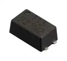


APV1111GVY
MOSFET Relay, SPST-NO (1 Form A), 8.5 V, 45 µA, SSOP-4, Surface Mount
- Manufacturer: PANASONIC
- Product type: MOSFET Solid State Relays
- SVHC: To Be Advised
- Load Type: -
- Contact Form: SPST-NO (1 Form A)
- Load Current: 45µA
- Product Range: APV Series
- Relay Mounting: Surface Mount
- Relay Terminals: Solder
- Load Voltage Max: 8.5V
- Isolation Voltage: 1.5kV
- I/O Capacitance Typ: 0.8pF
- On State Resistance Max: -
- MOSFET Relay Package Style: SSOP-4
- Off State Leakage Current Max: -
| Delivery and price | |
|---|---|
| Units per pack | 50 |
| Price | 2.82 € |
| Current stock | 10+ |
| Lead time | 30 days |
**==> picture [97 x 43] intentionally omitted <==**

## Photovoltaic MOSFET driver high power type

Product Catalog

**==> picture [503 x 423] intentionally omitted <==**

2022.4

## **Photovoltaic MOSFET driver high power type**

## **MOSFET drivers for high-speed operation and low on-resistance**

**==> picture [413 x 195] intentionally omitted <==**

**----- Start of picture text -----**<br>
P FEATURES o<br>Miniature SSOP package<br>High-speed MOSFET operation<br>(high output current: APV1111GV)<br>2.65 4.45 Low on-resistance of MOSFET<br>1.8 (high output voltage: APV3111GV)<br>© e<br>P TYPICAL APPLICATIONS o<br>+<br>1 4 Driving MOSFET<br>Measuring equipment, Testing equipment,<br>Industrial machinery, Industrial equipment,<br>ー<br>2 3 Data center, FA power supply<br>Note: Please contact our sales representative for automotive applications of PhotoMOS.<br>(Unit: mm)<br>Control circuit<br>**----- End of picture text -----**<br>


## | **TYPES**

|Package|Output rating|Output rating|Part No.|Part No.|Packing quantity|
|---|---|---|---|---|---|
||Drop-out voltage<br>(Typ. )|Short circuit current<br>(Typ. )|Surface-mount terminal||tape and reel|
||||Tape and reel<br>packingstyle Y *|Tape and reel<br>packingstyle1Y||
|SSOP|8.5V|45μA|APV1111GVY|APV1111GV1Y|Packing style Y<br>1-reel:3,500pcs.<br>Outer carton:3,500pcs.<br>Packing style1Y<br>1-reel:1,000pcs.<br>Outer carton:1,000pcs|
||18V|12μA|APV3111GVY|APV3111GV1Y||


- Tape and reel package is the standard packing style.

For space reasons, the two initial letters of the part number “AP”, package (SSOP) indicator “V” and the packing style are not marked on the device.

(Ex. the label for product number APV1111GVY is V1111G)

Tape and reel packing style picked from the 1/4-pin side.Tape and reel packing picked from 2/3-pin side is also available. Please contact our sales representative.

## Pe **RATING**

|Item|Item|Symbol<br>~~a~~|APV1111GV|APV3111GV|Remarks|
|---|---|---|---|---|---|
|Input|LED forward current<br>~~a~~|IF|30mA|||
||LED reverse voltage<br>~~eS~~<br>~~ee~~|VR<br>~~eS~~<br>~~ee ae~~|5V<br>~~eS~~<br>~~ae~~||~~ae~~|
||Peak forward current<br>~~eS~~<br>~~ee~~|IFP<br>~~eS~~<br>~~ee ae~~|1A<br>~~eS~~<br>~~ae~~||f =100Hz<br>DutyRatio =0.1%<br>~~ae~~|
||Power dissipation<br>~~ee~~<br>~~a~~|Pin<br>~~ee ae~~<br>~~a~~|60mW<br>~~ae~~<br>~~a~~||~~ae~~|
|I/O isolation voltage||Viso<br>~~a~~|1,500Vrms<br>~~a~~||~~a~~|
|Ambient temperature(Operating)||Topr<br>~~a~~|−40to+85°C<br>~~a~~||(Avoid icingand condensation)<br>~~a~~|
|Ambient temperature(Storage)||Tstg<br>~~a~~|−40to+100°C<br>~~a~~||~~a~~|
|Junction temperature||Tj<br>~~a~~<br>~~a~~|125°C<br>~~a~~<br>~~a~~||~~a~~<br>~~a~~|


Panasonic Industry Co., Ltd. Electromechanical Control Business Division industrial.panasonic.com/ac/e/

ASCTB437E   202204

ー 1 ー

Panasonic Industry Co., Ltd. 2022

Photovoltaic MOSFET driver high power type

## **Electrical characteristics (Ambient temperature: 25°C)**

**==> picture [512 x 363] intentionally omitted <==**

**----- Start of picture text -----**<br>
Item Symbol APV1111GV APV3111GV Condition<br>Typical 1.47 V<br>LED dropout voltage VF IF = 10 mA<br>Maximum 1.7 V<br>Typical 8.5 V 16.5 V IF = 5 mA<br>Drop-out voltage Minimum Voc 6 V 15 V<br>IF = 10 mA<br>Typical 8.5 V 18 V<br>Typical 25 µA 7 µA IF = 5 mA<br>Short circuit current Minimum Isc 25 µA 5 µA<br>IF = 10 mA<br>Typical 45 µA 12 µA<br>IF = 10 mA<br>Turn on time* Typical Ton 0.1 ms 0.4 ms CL = 1,000 pF<br>IF = 10 mA<br>Turn off time* Typical Toff 0.1 ms 0.04 ms CL = 1,000 pF<br>Typical 0.8 pF VB = 0 V<br>I/O capacitance Maximum Ciso 1.5 pF f = 1 MHz<br>Initial I/O isolation resistance Minimum Riso 1,000 MΩ 500 V DC<br>*Turn on/Turn off time measurement circuit<br>IF=10mA 1 4<br>VOUT<br>2 3 CL<br>CL=1000pF<br>* Turn on/Turn off time<br>Input<br>5V<br>1V<br>Output<br>Ton Toff<br>Input<br>Output<br>Transfer<br>characteristics<br>**----- End of picture text -----**<br>


## **Recommended operating conditions (Ambient temperature: 25°C)**

Please use under recommended operating conditions to obtain expected characteristics.

|Item|Symbol|Min.|Max.|Unit|
|---|---|---|---|---|
|LED forward current|IF|5|20|mA|


Panasonic Industry Co., Ltd. Electromechanical Control Business Division industrial.panasonic.com/ac/e/

ASCTB437E   202204

ー 2 ー

Panasonic Industry Co., Ltd. 2022

Photovoltaic MOSFET driver high power type

## **REFERENCE DATA**

**==> picture [511 x 589] intentionally omitted <==**

**----- Start of picture text -----**<br>
1-1.  Drop-out voltage vs. ambient 1-2.  Drop-out voltage vs. ambient 2-1.  Short circuit current vs. ambient<br>temperature characteristics temperature characteristics temperature characteristics<br>LED forward current: 10 mA; LED forward current: 10 mA; LED forward current: 10 mA;<br>Part No. : APV1111GV Part No. : APV3111GV Part No. : APV1111GV<br>14 27 75<br>12 24 60<br>10 21 45<br>8 18 30<br>6 15 15<br>4 12 0<br>-40 -20 0 20 40 60 8085 -40 -20 0 20 40 60 8085 -40 -20 0 20 40 60 8085<br>Ambient temperature (°C) Ambient temperature (°C) Ambient temperature (°C)<br>2-2.  Short circuit current vs. ambient 3.  LED dropout voltage vs. ambient 4.  Turn on time vs. ambient temperature<br>temperature characteristics temperature characteristics characteristics<br>LED forward current: 10 mA; LED forward current: 5 to 30 mA LED forward current: 10 mA;<br>Part No. : APV3111GV Load capacity: 1,000 pF;<br>Output voltage: 5 V<br>25 2.0 0.75<br>20 1.8 0.60<br>APV3111GV<br>15 1.6 0.45<br>30mA<br>20mA<br>10 1.4 10mA 0.30<br>5mA<br>5 1.2 0.15<br>APV1111GV<br>0 1.0 0<br>-40 -20 0 20 40 60 8085 -40 -20 0 20 40 60 8085 -40 -20 0 20 40 60 8085<br>Ambient temperature (°C) Ambient temperature (°C) Ambient temperature (°C)<br>5.  Turn off time vs. ambient temperature 6.  Turn on time vs. LED forward current 7.  Turn off time vs. LED forward current<br>characteristics characteristics characteristics<br>LED forward current: 10 mA; Load capacity: 1,000 pF; Load capacity: 1,000 pF;<br>Load capacity: 1,000 pF; Output voltage: 5 V; Output voltage: 1 V;<br>Output voltage: 1 V Ambient temperature: 25℃ Ambient temperature: 25℃<br>0.5 3.0 0.5<br>2.5<br>0.4 0.4<br>2.0<br>0.3 0.3<br>1.5<br>0.2 0.2<br>1.0<br>APV1111GV APV3111GV APV1111GV<br>0.1 0.1<br>0.5 APV1111GV APV3111GV<br>APV3111GV<br>0 0 0<br>-40 -20 0 20 40 60 80 85 0 5 10 15 20 25 30 0 5 10 15 20 25 30<br>Ambient temperature (°C) LED forward current (mA) LED forward current (mA)<br>Drop-out voltage (V) Drop-out voltage (V)<br>Short circuit current (μA)<br>Turn on time (ms)<br>Short circuit current (μA) LED dropout voltage (V)<br>Turn off  time (ms) Turn on  time (ms) Turn off  time (ms)<br>**----- End of picture text -----**<br>


Panasonic Industry Co., Ltd. Electromechanical Control Business Division industrial.panasonic.com/ac/e/

ASCTB437E   202204

ー 3 ー

Panasonic Industry Co., Ltd. 2022

## Photovoltaic MOSFET driver high power type

**==> picture [496 x 379] intentionally omitted <==**

**----- Start of picture text -----**<br>
8.  Turn on time vs. load capacitance 9.  Turn off time vs. load capacitance 10.  Drop-out voltage vs. LED forward<br>characteristics characteristics current characteristics<br>LED forward current: 10 mA; LED forward current: 10 mA; Ambient temperature: 25℃<br>Load capacitance: 100 pF to 10,000 pF; Load capacitance: 100 pF to 10,000 pF;<br>Output voltage: 5 V; Ambient temperature: 25℃ Output voitage: 1V; Ambient temperature: 25℃<br>10.00 10.00 25<br>PE ee<br>0 2 20 APV3111GV<br>APV3111GV<br>1.00 1.00<br>15<br>PO aA a<br>Ht a I APV1111GV fo APV1111GV fle | 10 APV1111GV<br>0.10 0.10<br>PT PA TT ee 5<br>Panel APV3111GV ee<br>0.01 ee 0.01 H ill it LL 0<br>100 1,000 10,000 100 1,000 10,000 0 5 10 15 20 25 30<br>Load capacitanse (pF) Load capacitanse (pF) LED forward current (mA)<br>11.  Short circuit current vs. LED forward<br>current characteristics<br>Ambient temperature: 25℃<br>1,000<br>Yt tT TTT<br>APV1111GV<br>100<br>a 7A<br>APV3111GV<br>10<br>>A<br>1 I Co<br>1 10 100<br>LED forward current (mA)<br>Turn on  time (ms) Turn off  time (ms) Drop-out voltage (V)<br>Short circuit current (μA)<br>**----- End of picture text -----**<br>


## i **DIMENSIONS** «= **CAD** The CAD data of the products with a “CAD” mark can be downloaded from our Website.

Unit: mm

**==> picture [488 x 250] intentionally omitted <==**

**----- Start of picture text -----**<br>
|_| SSOP<br>Ga» CAD External dimensions Recommended mounting pad<br>4.45 (TOP VIEW)<br>0.9<br>we r i t —_ 1.27<br>4.35<br>0.2 0.2 0.4 0.4<br>Tolerance: ±0.1<br>(4.85) 1.27<br>Terminal thickness: t = 0.15<br>General tolerance: ±0.1<br>el SCHEMATIC AND WIRING DIAGRAMS<br>Schematic confiOutputguration Load type Connection Wiring diagram<br>1 +4 IF 1 4 Load 4 Load +<br>1 Form A - - E1 ExternalMOSFET VL (AC, DC) ExternalMOSFET VL (DC)<br>2 - 3 e 2 T 3 Re [E 3 P -<br>HH _ L__|<br>2.65 0.7<br>1.8<br>Control circuit<br>**----- End of picture text -----**<br>


Panasonic Industry Co., Ltd. Electromechanical Control Business Division industrial.panasonic.com/ac/e/

ASCTB437E   202204

ー 4 ー © Panasonic Industry Co., Ltd. 2022

Photovoltaic MOSFET driver high power type

## **SAFETY STANDARDS**

**==> picture [512 x 58] intentionally omitted <==**

**----- Start of picture text -----**<br>
UL (Recognized)<br>Part No. File No. Remarks<br>(Standard No.) Contact rating<br>APV1111GV E191218 ー<br>MOSFET driver<br>APV3111GV (UL1577) ー<br>**----- End of picture text -----**<br>


Note: For the latest information on compliance with safety standards, please refer to our website.

Please refer to **"the latest product specifications"** when designing your product.

- •Requests to customers: https://industrial.panasonic.com/ac/e/salespolicies/

Panasonic Industry Co., Ltd. Electromechanical Control Business Division industrial.panasonic.com/ac/e/

ASCTB437E   202204

Panasonic Industry Co., Ltd. 2022

ー 5 ー

**PhotoMOS[®] Cautions for Use**

## **SAFETY WARNINGS**

Do not use the product under conditions that exceed the range

## [Lo **PhotoMOS[®] Cautions for Use** ~~|_|~~ **Derating design**

**==> picture [235 x 63] intentionally omitted <==**

**----- Start of picture text -----**<br>
6) When storing or transporting PhotoMOS, ® the environment should<br>not be conducive to generating static electricity (for instance, the<br>humidity should be between 45% and 60%), and PhotoMOS ®<br>should be protected using conductive packing materials.<br>Unused terminals<br>**----- End of picture text -----**<br>


## **Short across terminals**

**==> picture [224 x 20] intentionally omitted <==**

**----- Start of picture text -----**<br>
 Applying stress that exceeds the absolute maximum<br>rating<br>**----- End of picture text -----**<br>


## **Surge voltages at the input**

**==> picture [225 x 19] intentionally omitted <==**

**----- Start of picture text -----**<br>
Input voltage (for Voltage-sensitive type)<br>For rising and dropping ratio of input voltage(dv/dt), maintain Min.<br>**----- End of picture text -----**<br>


**==> picture [213 x 9] intentionally omitted <==**

**----- Start of picture text -----**<br>
Oscillation circuit and control circuit (for CC Type)<br>**----- End of picture text -----**<br>


**Deterioration and destruction caused by discharge of static electricity** This phenomenon is generally called static electricity destruction, and occurs when static electricity generated by various factors is dischargedinternal destructionwhile theofPhotoMOS the element. ® terminals are in contact, producing To prevent problems from static electricity, the following precautions and measures should be taken when using your device. 1) Employees handling PhotoMOS ® should wear anti-static clothing

**==> picture [119 x 192] intentionally omitted <==**

**----- Start of picture text -----**<br>
| 1 6<br>2 5<br>x<br>3 4<br>O<br> type<br>Te<br>— O 3 O 4<br>O @ O<br>1 2<br>**----- End of picture text -----**<br>


## **Reverse voltages at the input (for CC Type)**

**==> picture [271 x 75] intentionally omitted <==**

**----- Start of picture text -----**<br>
O 1 4 O<br>® zr 2 | 3<br>0 0<br>ー 6 ー © Panasonic Industry Co., Ltd. 2023 ASCTB65E   202302<br>**----- End of picture text -----**<br>


Panasonic Industry Co., Ltd. Electromechanical Control Business Division industrial.panasonic.com/ac/e/

## PhotoMOS[®] Cautions for Use ~~eec~~ reer rere reer c **e** ce ~~|~~ **Recommended LED forward current or recommended input voltage**

**==> picture [154 x 45] intentionally omitted <==**

**----- Start of picture text -----**<br>
within ±0.5 V<br>~ po<br>Set voltage<br>| ae<br>LKAS aVALV ALY, 7” q t<br>within ±0.5 V<br>**----- End of picture text -----**<br>


## **LED forward current vs. Ambient temperature characteristics**

## **Output spike voltages**

**==> picture [457 x 544] intentionally omitted <==**

**----- Start of picture text -----**<br>
Oo 1 6<br>100 @<br>Oo 2 5 O<br>80 Load<br>° 3 4<br>a<br>60 Clamp diode is<br>connected in parallel<br>with the load.<br>40<br>| 20 @OO 12 65 O Q<br>Load<br>3 4<br>0-40 -20 0 20 40 60 8085 100 O TO<br>L_]<br>Ambient temperature (°C) CR snubber is<br>connected in parallel<br>For AQV209G, APV1111GV, APV3111GV with the load.<br>50<br>(2) Power type<br>40<br>30<br>1 2 3 4<br>o® O Load<br>20 Clamp diode is<br>connected in parallel<br>with the load.<br>10<br>0 1 2 3 4<br>-40 -20 0 20 40 60 80 85 100<br>Ambient temperature (°C) O00 Load CR snubber is<br>HOF connected in parallel<br>with the load.<br>Ripple in the input power supply<br>If ripple is present in the input power supply, observe the following:<br>1 2 3 4<br>1) For LED forward ■ current at Emin, please maintain the value r e<br>Load A varistor is<br>2) Pleasementionedmakeat “sureRecf o rmmended LEDthe LED forwad forwacu r rentd current.”at Emax. is less 6@d Pe Str Y connected in parallel<br>than the current value of the “■ | Absolute maximum ratings ” . with PhotoMOS [®]<br>3) Please maintain the input voltage at least 4V for Emin. (GU, RF (3) CC Type<br>and Power voltage-sensitive type). 1 4<br>4) Please make sure the input voltage for Emax. is no higher than 6V<br>Load<br>(GU and RF voltage-sensitive type). Oo 2 3 Sa<br>5) Please make sure the input voltage for Emax. is no higher than 30V Saeed<br>(Power voltage-sensitive type). Clamp diode is<br>6) Please maintain the input voltage at least 3V for Emin. connected in parallelwith the load.<br>(for CC Type)<br>1 4<br>7) Please make sure the input voltage for Emax. is no higher than 5.5V.<br>Load<br>2 3<br>(for CC Type) 5 iw<br>CR snubber is<br>connected in parallel<br>Emin. Emax. with the load.<br>LED forward current (mA)<br>LED forward current (mA)<br>**----- End of picture text -----**<br>


Panasonic Industry Co., Ltd. Electromechanical Control Business Division industrial.panasonic.com/ac/e/

ASCTB65E   202302

Panasonic Industry Co., Ltd. 2023

ー 7 ー

## PhotoMOS[®] Cautions for Use ~~eec~~ reer rere reer c **e** ce **Output Waveform (CC Type)** ~~|~~ **Input wiring pattern**

## specified I/O isolation voltage (V_) so after mounting the PC board.

## **Continual DC bias (AQV259 and AQV258)**

**==> picture [167 x 66] intentionally omitted <==**

**----- Start of picture text -----**<br>
1 6<br>E  IF<br>2 5 IL<br>=<br>3 4<br>Load<br>eS<br>**----- End of picture text -----**<br>


**==> picture [211 x 126] intentionally omitted <==**

**----- Start of picture text -----**<br>
Portion of output side frame<br>\\ (Output terminal side) a,<br>c s<br>I E<br>Input wiring L E ats -<br>pattern (Input terminal side)<br>May not allow the prescribed I/O withstand<br>voltage (Viso) to be achieved<br>Se<br>packages<br>* Excluding high I/O isolation voltage products and SSOP, SON, and TSON<br>**----- End of picture text -----**<br>


## **Connections Between Input and Output (CC Type)**

**==> picture [164 x 41] intentionally omitted <==**

**----- Start of picture text -----**<br>
1 4<br>VIN IIN IL VL(AC, DC)<br>Load<br>2 3<br>**----- End of picture text -----**<br>


## **Cleaning solvents compatibility**

* Ultrasonic output: No greater than 0.25W/cm 2 *

## **Notes for mounting**

## ■

®

Panasonic Industry Co., Ltd. Electromechanical Control Business Division industrial.panasonic.com/ac/e/

ー 8 ー

ASCTB65E   202302

Panasonic Industry Co., Ltd. 2023

## PhotoMOS[®] Cautions for Use

## **Soldering**

**==> picture [228 x 129] intentionally omitted <==**

**----- Start of picture text -----**<br>
t 3<br>T 3 T1 = 150 to 180°C<br>T2 = 230°C<br>T 2 T3 = 240 to 250°C*<br>t1 = 60 to 120 s<br>T 1 t2 = Within 30 s<br>t3 = Within 10 s<br>*240 to 245°C for SON, VSSOP<br>  and TSON package<br>t 1 t 2<br>(2) Other soldering methods<br>Other soldering methods (VPS, hot-air, hot plate, laser<br>®<br>**----- End of picture text -----**<br>


**==> picture [212 x 66] intentionally omitted <==**

**----- Start of picture text -----**<br>
T 2 T1 = 120°C<br>T2 = Max. 260°C<br>t1 = within 60 s<br>T 1<br>t2+t3 = within 5 s<br>t 1 t 2 t 3<br>**----- End of picture text -----**<br>


**==> picture [49 x 9] intentionally omitted <==**

**----- Start of picture text -----**<br>
soldering lead<br>**----- End of picture text -----**<br>


## **About the exposed terminals on the sides of the package (for VSSOP)**

**==> picture [232 x 395] intentionally omitted <==**

**----- Start of picture text -----**<br>
internal element, please refer to the item “ ■ Deterioration and<br>destruction caused by discharge of static electricity’, and<br>implement sufficient measures to control static electricity.<br>3) When installing the devices in the vicinity, please keep in mind<br>that if the exposed frames of adjacent devices get too close, a<br>short between devices may occur.<br>Part of frame on output side<br>Part of frame on input side Va besa<br>Adjacent mounting<br>When several PhotoMOS ® are mounted closely each other or<br>heat-generating components are mounted close to the PhotoMOS ®<br>the abnormal heating may occur. This abnormal heat may be<br>caused by the internal element when energized or thermal<br>interference between the devices. The degree of temperature rise<br>depends on the mounting layout of the devices and usage condition,<br>therefore please be sure to use PhotoMOS ® with reduced load<br>current after testing under the worst condition of the actual usage.<br>Transportation and storage<br>1) Extreme vibration during transport may deform the lead or<br>damage the PhotoMOS ® characteristics. Please handle the outer<br>and inner boxes with care.<br>2) Inadequate storage conditionwomay degrade soldering,. wae<br>appearance, and characteristics. The following storage conditions<br>are recommended:<br>* Temperature: 0 to 45°C<br>* Humidity: Max. 70%RH<br>.<br>+ Atmosphere: Noiharmful gasses such as sulfurous acid gas,<br>minimal dust. .<br>3) Storage before TSON, VSSOP, SON, SSOP, or SOP processing ®<br>**----- End of picture text -----**<br>


## **Water condensation**

- ®

®

Panasonic Industry Co., Ltd. Electromechanical Control Business Division

ー 9 ー © Panasonic Industry Co., Ltd. 2023

ASCTB65E   202302

industrial.panasonic.com/ac/e/

PhotoMOS[®] Cautions for Use

## **About foreign matter between the output terminals (AQY206GV)**

Panasonic Industry Co., Ltd. Electromechanical Control Business Division industrial.panasonic.com/ac/e/

ー 10 ー © Panasonic Industry Co., Ltd. 2023

ASCTB65E   202302

## PhotoMOS[®] Cautions for Use

**==> picture [76 x 25] intentionally omitted <==**

**----- Start of picture text -----**<br>
| Packing format<br>1) Tape and reel<br>**----- End of picture text -----**<br>


**==> picture [484 x 696] intentionally omitted <==**

**----- Start of picture text -----**<br>
Direction of picking<br>Tractor feed holes 1.5 ー [+0.1] 0 dia. 21 [±][0.8]<br>0.2 [±][0.05] 2.2 [±][0.2] 4 [±][0.1]<br>2 [±][0.5]<br>| LI |<br>Device mounted<br>4-pin on tape<br>r 1.2 [±][0.3] eT AT 1.05 TTT ±0.1dia. LU i 2 [±][0.1] Wai,<br>4±0.1<br>( 1 ) When picked from 1 2 / -pin side: Part No. AQY 2 C*R*PX, 13 [±][0.5] dia.<br>AQY 2 C*R*P 1 X (Shown above) 13 [±][1.5] 1.2±0.5<br>() 2 When picked from 3 4 / -pin side: Part No. AQY 2 C*R*PZ *Quality of material: Polystyrene (PS)<br>21 [±][0.8]<br>Direction of picking<br>80 [±][1] dia.<br>Tractor feed holes 1.5 +0.1ー0 dia.<br>0.4 [±][0.05] 2.4±0.2 4.0 [±][0.1]<br>| a | 2 [±][0.5]<br>Device mounted Ha_(cel_tept (eat !<br>4-pin on tape<br>3.3 [±][0.3] 1±0.1dia. Lt 8 [±][0.1] 2 [±][0.1]<br>(_) 12 When picked from 12 and  and 43 -pin side: Part No. AQY * TY * (Shown above) *Quality of material: Paper 13 [±][0.5] dia. 14±1.5 2 [±][0.5]<br>(_) When picked from -pin side: Part No. AQY TW — HL. —<br>End of the part number Y/W<br>Direction of picking 21 [±][0.8]<br>Tractor feed holes 1.5  [+0.1] ー0 dia. 80 [±][1] dia.<br>0.3 [±][0.05] 2.8 [±][0.2] 4 [±][0.1]<br>|||<br>2 [±][0.5]<br>‘hohe a ¥<br>Device mounted<br>4-pin on tape<br>Hl SN K<br>2 [±][0.3] 1.5 [±][0.1] dia. 4 [±][0.1] 2 [±][0.1]<br>La wy, eS<br>(_) 1 When picked from 1 and 4 -pin side: Part No. AQY * MY,<br>AQY*M 1 Y (Shown above)<br>(_) 2 When picked from 2 and 3 -pin side: Part No. AQY * MW<br>*Quality of material: Paper 13 [±][0.5] dia. 14±1.5 2 [±][0.5]<br>Direction of picking<br>Tractor feed holes 1.5 ー [+0.1] 0 dia. End of the part number 1 Y<br>0.3 [±][0.05] 3.0 [±][0.1] 4.0 [±][0.1]<br>| | _ | | 21 [±][0.8]<br>- i 2 [±][0.5]<br>SSOP Ls Device mounted He AN ATS<br>4-pin on tape<br>2.7 [±][0.3] 4.0 [±][0.1]<br>1.5ー [+0.1] 0 dia.<br>(_) 1 When picked from 1 and 4 -pin side: PartNo. QY*VY,AQY 221 “*V/Y, 1<br>APV* 111 *VY,<br>APV* 111 *V 1 Y (Shown above) 13 [±][0.5] dia.<br>(_) 2 When picked from 2 and 3 -pin side: Part No. AQY*VW, APV* 111 *VW *Quality of material: Polystyrene (PS) 13 [±][1.5] 1.2±0.5<br>21 [±][0.8]<br>Direction of picking 80 [±][1] dia.<br>Tractor feed holes<br>0.3 [±][0.05] 1.5 a +0.1ー0 dia. : P| 7.2 ±0.1 2 [±][0.5]<br>P ee; tH Tt K<br>4-pin Device mounted on tape<br>| 2.8  [±][0.3] ) i 4  [±][0.1] 1.55 [±][0.1] dia. e<br>te 12  [±][0.1] i 2 [±][0.1] Vy,<br>(_) 1 When picked from 1 2 / -pin side: Part No. AQY*SX, APV** 21 SX (Shown above)<br>() 2 When picked from 3 4 / -pin side: Part No. AQY*SZ, APV** 21 SZ *Quality of material: Paper 13 [±][0.5] dia. 14±1.5 2 [±][0.5]<br>*  ” indicates characters of number or alphabet.<br>0.1<br>±1.75<br>0.2<br>±2.4 +0.3120.1ー 3±dia. 3±dia.<br>60 180<br>0.1<br>±<br>5.5<br>0.1±<br>0.2±2.5 1.75<br>+0.312.00.1ー ±dia.1 2±dia.<br>80 250<br>0.1±5.5<br>0.1±1.75<br>0.2±3.6<br>0.3±12<br>0.1± ±dia.180 2±dia.250<br>5.5<br>0.1±<br>0.2±5.1 1.75<br>0.1±5.5 +0.312.00.1ー 3±dia. 3±dia.<br>60 180<br>0.1±<br>1.75<br>0.1± 0.1±5.5  +0.3 0.1ー<br>4.7  12 ±dia.1 2±dia.<br>80 250<br>**----- End of picture text -----**<br>


Panasonic Industry Co., Ltd. Electromechanical Control Business Division

industrial.panasonic.com/ac/e/

ASCTB65E   202302

ー 11 ー

Panasonic Industry Co., Ltd. 2023

## PhotoMOS[®] Cautions for Use

**==> picture [498 x 708] intentionally omitted <==**

**----- Start of picture text -----**<br>
21 [±][0.8]<br>80 [±][1] dia.<br>Direction of picking<br>0.3  [±][0.05] Tractor feed holes1.5 +0.1ー0 dia. 4 ±0.1 7.2 ±0.1<br>2 [±][0.5]<br>tt | [dt] i<br>>t es  e e gw ’<br>6 . -pin i Device mounted on tape (aI YJ x<br>12  [±][0.1] 2 [±][0.1] 1.55 [±][0.1] dia.<br>2.8  5 [±][0.3] Yael TINA o Hs<br>((_) 12 )When When pickedpicked fromfrom 1 2 34 //5// 6 -pin-pin side:side: PartPart No.No. AQV*SZ AQV*SX (Shown above) *Quality of material: Paper 13 [±][0.5] dia. 14±1.5 | ||— 2 [±][0.5]<br>Direction of picking<br>0.3  [±][0.05] Tractor feed holes1.5 +0.1ー0 dia. 7.5 ±0.1<br>a |<br>-pin Device mounted 21±0.8<br>8> ul on tape eaciker LE = 80 [±][1] dia.<br>4  [±][0.1] 1.55 [±][0.1] dia.<br>2.8  [±][0.3]<br>= 12  [±][0.1] 2 [±][0.1]<br>2 [±][0.5]<br>(_) 1 When picked from 1 2 3 4 / / / -pin side: Part No. AQW*SX (Shown above) jul<br>(_) 2 When picked from 5/ 6 7 / /8-pin side: Part No. AQW*SZ ag<br>Direction of picking<br>Tractor feed holes<br>| 0.3  [±][0.05] 1.5 +0.1ー0 dia. 7.5  [±][0.1]<br>= X ae i re a |<br>Device mounted *Quality of material: Paper 13 [±][0.5] dia. 17.5 [±][1.5] 2 [±][1]<br>16-pin i on tape VEE (ETT IA S<br>4  [±][0.1] 1.55 [±][0.1] dia.<br>2.8  [±][0.3] = 12  [±][0.1] if 2 [±][0.1]<br>() 1 When picked from 1 2 3 4 / / / /5/ 6 7 / /8-pin side: Part No. AQS*SX (Shown above)<br>( 2 ) When picked from 9/ 10 11 12 13 14 / / / / /15/ 16 -pin side: Part No. AQS*SZ<br>21 [±][0.8]<br>80 [±][1] dia.<br>Direction of picking<br>0.3 ±0.05 Tractor feed holes1.5+0.1ー0 dia. 4  [±][0.1] 10.2  [±][0.1] 2 [±][0.5]<br>DIP 4-pin ft —_ ot dy<br>Surface {=a RSS gi SN Axe<br>terminal mount | [f ES Device mounted on tape feanlawe Pe  USSTZ t | Se<br>LJ 12  [±][0.1] 2 [±][0.1] 1.55 [±][0.1] dia.<br>4.2  [±][0.3]<br>( 1 ) When picked from 1 2 / -pin side: Part No. AQY*HAX, AQY 210 — HLAX (Shown above) *Quality of material: Paper 13 [±][0.5] dia. 13.5 [±][2.0] 2±0.5<br>( 2 ) When picked from 3 4 / -pin side: Part No. AQY*HAZ, AQY 210 ~HLAZ<br>21±0.8<br>80 [±][1] dia.<br>Direction of picking<br>0.3  [±][0.05] Tractor feed holes1.5 [+0.1] ー0 dia. 10.1 ±0.1 2±0.5<br>6-pin<br>DIP 5 aq] ye | f<br>Device mounted on tape<br>terminal =I Set fob} JLIN S<br>— J 12  [±][0.1] 4  [±][0.1] 1.6 [±][0.1] dia.<br>4.5  [±][0.3] 2 [±][0.1]<br>( 1 ) When picked from 1 2 3 / / -pin side: Part No. AQV*AX (Shown above) *Quality of material: Paper 13±0.5dia. 17.5 [±][2] 2 [±][0.5]<br>(_) 2 When picked from 4 /5/ 6 -pin side: Part No. AQV*AZ<br>“ *  ” indicates characters of number or alphabet.<br>0.1±<br>1.75<br>6.90.1± 0.1±5.5  +0.3120.1ー ±dia.1 2±dia.<br>80 250<br>0.1±<br>1.75<br>0.1± 0.1±57. +0.3 0.1ー<br>16<br>10.15<br>±1dia. 2±dia.<br>80 250<br>0.1±1.75<br>0.1± 0.1±7.5  +0.3 0.1ー<br>11.15  16<br>0.1±1.75<br>0.1± 0.1±5.5  +0.3120.1ー  ±1dia. 2±dia.<br>5.25  80 300<br>0.1±<br>1.75<br>0.1±2 0.1±7.5  +0.3160.1ー ±1dia. 2±dia.<br>9. 80 300<br>**----- End of picture text -----**<br>


Panasonic Industry Co., Ltd. Electromechanical Control Business Division industrial.panasonic.com/ac/e/

ASCTB65E   202302

ー 12 ー

Panasonic Industry Co., Ltd. 2023

**==> picture [145 x 11] intentionally omitted <==**

**----- Start of picture text -----**<br>
PhotoMOS [®]  Cautions for Use<br>**----- End of picture text -----**<br>


**==> picture [500 x 549] intentionally omitted <==**

**----- Start of picture text -----**<br>
Direction of picking<br>Tractor feed holes<br>>| 0.3  [±][0.05] 1.5 [+0.1] ー0 dia. _ 4  ft [±][0.1] 10.1 ±0.1<br>\ im<br>-pin<br>21±0.8<br>Device mounted on tape<br>terminal =I 2a: LY LLI N 80 [±][1] dia.<br>12  [±][0.1] 2 [±][0.1] 1.55 [±][0.1] dia.<br>4.5±0.3<br>2±0.5<br>( 1 ) When picked from 1 2 3 4 / / / -pin side: Part No. AQW*AX (Shown above) th<br>(_) 2 When picked from 5/ 6 7 / /8-pin side: Part No. AQW*AZ ws<br>Direction of picking<br>Tractor feed holes<br>DIP 8 -pin > 0.3 ±0.05 1.5 \G=$—9 +0.1ー0 dia.  Reft 4  [±][0.1] | 10.2 ±0.1<br>Surface mount fa |<br>*Quality of material: Paper 13±0.5dia. 17.5 [±][2] 2 [±][0.5]<br>voltage isolation  terminalHigh /O type a 4.2  | 2) [±][0.3] Device mounted on tape Seb |__| 12 ± HH LL 0.1 L 2 [±] LL [0.1] KT 1.55 [±][0.1] dia. He<br>( 1 ) When picked from 1 2 3 4 / / / -pin side: Part No. [AQW*EHAX,]<br>AQW 210 — HLAX (Shown above)<br>( 2 ) When picked from 5/ 6 7 / /8-pin side: Part No. AQW*EHAZ, AQW 210 ~— -HLAZ<br>21±0.8<br>100 [±][1] dia.<br>Direction of picking<br>0.3 ±0.05 Tractor feed holes1.5 +0.1ー0 dia. 4.0 ±0.1 12.6 ±0.1 2 [±][0.5]<br>Power-DIP || Aus<br>4-pin<br>© © op<br>Device mounted<br>on tape<br>16.0±0.1 2.0±0.1 1.55±0.1dia.<br>4.5  a . ±0.3 Ls<br>(( 12 )) When When pickedpicked fromfrom 1 23 4 // -pin-pin side:side: PartPartNo.No. AQY AQY ** AXAZ(Shown above) *Quality of material: Paper 13 [±][0.5] dia. 25.5 [±][2] 1.7 [±][0.8]<br>21±0.8<br>80 [±][1] dia.<br>Direction of picking<br>0.3  [±][0.05] Tractor feed holes1.5+0.1ー0 dia. 10.1 ±0.1<br>3 2±0.5<br>6-pin<br>DIP ATA Vy 4<br>Surface mount Fl . (i ] (i V ie<br>Device mounted on tape<br>(Photovoltaic = I = 12 ±0.1 4 ±0.1 m Y 1.6 [±][0.1] dia.<br>MOSFET driver) 4.5  [±][0.3] J_JL 2±0.1 J<br>( 1 ) When picked from 1 2 3 / / -pin side: PartNo.APV 1122 = AX (Shown above) *Quality of material: Paper 13±0.5dia. 17.5 [±][2] 2 [±][0.5]<br>( 2 ) When picked from 4 6 / -pin side: PartNo.APV 1122 AZ a<br>*<br>0.1±<br>1.75<br>0.1± 0.1±7.5 +0.3 0.1ー<br>10.2  16<br>±1dia. 2±dia.<br>80 300<br>0.1±<br>1.75<br>0.1± 0.1±7.5  +0.3 0.1ー<br>10.3  16<br>0.1±1.75<br>0.1±9.7 0.1±11.5 0.3 ±24.0 ±1dia.100 2±330dia.<br>0.1±1.75<br>0.1±9.2 0.1±7.5  +0.3160.1ー ±1dia. 2±dia.<br>80 300<br>**----- End of picture text -----**<br>


**==> picture [125 x 51] intentionally omitted <==**

**----- Start of picture text -----**<br>
— Stopper B Stopper A<br>S77<br>to  (roan rrr<br>(DIP type)<br>Stopper<br>**----- End of picture text -----**<br>


**==> picture [154 x 74] intentionally omitted <==**

**----- Start of picture text -----**<br>
@ ===<br>Stopper B (green) Stopper A (gray)<br>—_— A<br>(Power type)<br>Stopper B Stopper A<br>PN<br>**----- End of picture text -----**<br>


Panasonic Industry Co., Ltd. Electromechanical Control Business Division industrial.panasonic.com/ac/e/

ASCTB65E   202302

ー 13 ー

Panasonic Industry Co., Ltd. 2023

**==> picture [134 x 42] intentionally omitted <==**

Electromechanical Control Business Division 1006, Oaza Kadoma, Kadoma-shi, Osaka 571-8506, Japan industral.panasonic.com/ac/e/

Specifications are subject to change without notice. ASCTB437E   202204

©Panasonic Industry Co., Ltd. 2022

2022.4
Updated at June 6, 2026
Panasonic Industry is a global leader in the design and manufacture of high-quality electronic components. Renowned for a commitment to continuous innovation, the company provides the essential building blocks that empower modern engineering. From industrial automation to consumer electronics, Panasonic's components are trusted worldwide for their outstanding reliability, efficiency, and long-term performance. The extensive portfolio is anchored by a massive selection of passive components, featuring an industry-leading range of aluminium electrolytic, film, and polymer capacitors. Alongside these advanced capacitance solutions, engineers rely on Panasonic's robust power inductors and a highly versatile array of electromechanical devices, including solid-state, power, and signal relays engineered to excel in demanding environments. Beyond core passives and switching solutions, the offering encompasses critical circuit protection devices such as TVS varistors and NTC thermistors, as well as sophisticated thermal management materials. Panasonic also delivers precision light and motion sensors, highly reliable batteries, and advanced Bluetooth and WLAN connectivity modules, providing a comprehensive ecosystem of components to support next-generation technological design.
About Novapart
Novapart is a B2B electronic component broker specialising in stock shortages and cost reduction. We source hard-to-find parts and identify compliant alternatives across a catalogue of 410,000+ components from 500+ manufacturers.
Learn more →Stock Shortage Specialist
When a component is unavailable, discontinued or has an unacceptable lead time, we tap into our network of vetted European and Asian distributors to source what you need — without compromising on quality or traceability.
Request a quote →Compliant Alternatives
We identify pin-to-pin, electrically equivalent substitutes that meet the same certifications (RoHS, AEC-Q100, REACH) as your original specification — validated against datasheets, not just part numbers. Often at a lower cost.
BOM Analysis service →