
Image not available
Illustrative purposes only

APT13003NZTR-G1
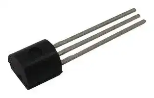
Bipolar (BJT) Single Transistor, NPN, 530 V, 1.5 A, 1 W, TO-92, Through Hole
⚠️ Reference pricing provided. In case of supply shortages, we will connect you with our trusted procurement partners to ensure your project's continuity.
- Manufacturer: DIODES INC.
- Product type:
- SVHC: No SVHC (15-Jan-2018)
- No. of Pins: 3Pins
- Product Range: -
- Qualification: -
- Power Dissipation: 1W
- Transistor Mounting: Through Hole
- Transistor Polarity: NPN
- Transition Frequency: 4MHz
- Transistor Case Style: TO-92
- DC Current Gain hFE Min: 5hFE
- Operating Temperature Max: 150°C
- Continuous Collector Current: 1.5A
- Collector Emitter Voltage Max: 530V
| Delivery and price | |
|---|---|
| Units per pack | 100 |
| Price | 0.164 € |
| Current stock | 10+ |
| Lead time | 30 days |
Datasheet

**APT13003NZ**

**530V NPN HIGH VOLTAGE POWER TRANSISTOR IN TO92**

## **Features**

## **Mechanical Data**

- BVCEO > 530V

- BVCES > 900V

- BVEBO > 10V

- IC = 1.5A high Continuous Collector Current

- High Switching Speed

- **Lead-Free Finish; RoHS Compliant (Notes 1 & 2)**

   - Case: TO92

   - Case Material: Molded Plastic, "Green" Molding Compound; UL Flammability Classification Rating 94V-0

   - Terminals: Matte Tin Finish; Solderable per MIL-STD-202, Method 208

   - Weight: 200mg (Approximate)

- **Halogen and Antimony Free. “Green” Device (Note 3)**

## **Applications**

Low Power AC-DC SMPS for:

- Battery Chargers for Mobile Phone / Tablets / Smartphones

- Power Supply for DVD / STB

- LED Lighting

**==> picture [383 x 123] intentionally omitted <==**

**----- Start of picture text -----**<br>
C<br>TO92<br>B<br>E  C  B  B  C  E<br>Flat Face View  Bottom View<br>E<br>Pin-Out<br>Device Schematic<br>**----- End of picture text -----**<br>


## **Ordering Information** (Note 4)

|**Ordering Informationg Information Information**(Note 4)||||
|---|---|---|---|
|**Product**|**Package **|**Marking**|**Quantity**|
|APT13003NZTR-G1|TO92(JoggledLegs)|13003NZ-G1|2,000Taped, per AmmoBox|


Notes: 1. EU Directive 2002/95/EC (RoHS) & 2011/65/EU (RoHS 2) compliant. All applicable RoHS exemptions applied.

2. See http://www.diodes.com/quality/lead_free.html for more information about Diodes Incorporated’s definitions of Halogen- and Antimony-free, "Green" and Lead-free.

3. Halogen- and Antimony-free "Green” products are defined as those which contain <900ppm bromine, <900ppm chlorine (<1500ppm total Br + Cl) and <1000ppm antimony compounds.

4. For packaging details, go to our website at http://www.diodes.com/products/packages.html.

## **Marking Information**

**==> picture [257 x 90] intentionally omitted <==**

**----- Start of picture text -----**<br>
  = Manufacturers’ Code Marking<br>13003N  13003NZ-G1 = Product Type Marking ID<br>Z-G1  YWW = Date Code Marking<br>YWW8XX  e.g. 512 = Year 2015, Week 12.<br>8 = Assembly Site Code<br>XX = Batch Number<br>Flat Face<br>View<br>**----- End of picture text -----**<br>


1 of 7 **www.diodes.com**

APT13003NZ Document number: DS37774 Rev. 1 - 2

July 2015 © Diodes Incorporated

**APT13003NZ**

## **Absolute Maximum Ratings** (@TA = +25°C, unless otherwise specified.)

|**Absolute Maximum Ratingsgss** (@TA = +25°C, unless otherwise specified.)A = +25°C, unless otherwise specified.)= +25°C, unless otherwise specified.)|(@TA = +25°C, unless otherwise specified.)A = +25°C, unless otherwise specified.)= +25°C, unless otherwise specified.)|||
|---|---|---|---|
|**Characteristic**|**Symbol**|**Value**|**Unit**|
|Collector-Emitter Voltage(VBE= 0V)|VCES|900|V|
|Collector-Emitter Voltage|VCEO|530|V|
|Emitter-Base Voltage|VEBO|10|V|
|Continuous Collector Current|IC|1.5|A|
|Peak Pulse Collector Current|ICM|3|A|
|Continuous Base Current|IB|0.75|A|
|Peak Pulse Base Current|IBM|1.5|A|


## **Thermal Characteristics** (@TA = +25°C, unless otherwise specified.)

|**Thermal Characteristics**(@TA = +25°C, unless otherwise specified.)A = +25°C, unless otherwise specified.)= +25°C, unless otherwise specified.)|(@TA = +25°C, unless otherwise specified.)A = +25°C, unless otherwise specified.)= +25°C, unless otherwise specified.)|||
|---|---|---|---|
|**Characteristic**|**Symbol**|**Value**|**Unit**|
|Power Dissipation|PD|1.0|W|
|Thermal Resistance, Junction to Ambient Air|RθJA|125|°C/W|
|Thermal Resistance, Junction to Case|RθJC|83.3|°C/W|
|Operatingand Storage Temperature Range|TJ,TSTG|-55 to +150|°C|


## **ESD Ratings** (Note 5)

|**ESD Ratingsgss **(Note 5)|**ESD Ratingsgss **(Note 5)|**ESD Ratingsgss **(Note 5)|**ESD Ratingsgss **(Note 5)|**ESD Ratingsgss **(Note 5)|
|---|---|---|---|---|
||||||
|**Characteristic**|**Symbol**|**Value**|**Unit**|**JEDEC Class**|
|Electrostatic Discharge - Human BodyModel|ESD HBM|8,000|V|3B|
|Electrostatic Discharge - Machine Model|ESD MM|400|V|C|


Note:      5.  Refer to JEDEC specification JESD22-A114 and JESD22-A115.

2 of 7 **www.diodes.com**

APT13003NZ Document number: DS37774 Rev. 1 - 2

July 2015 © Diodes Incorporated

**APT13003NZ** |

## **Thermal Characteristics and Derating Information** (@TA = +25°C, unless otherwise specified.)

**==> picture [448 x 345] intentionally omitted <==**

**----- Start of picture text -----**<br>
1 1.0<br>TO92 Package TO92 Package<br>See,J} |  See-\--_] | eeef+ 0.8 N\ NS<br>100m DC<br>EN 0.6 aN<br>| 0.4 Nee<br>10m<br>LU | 0.2 PTT PT PT NOT I<br>1m SEa ee | 0.0 Pet ot ttt LNG \<br>1 10 100 0 20 40 60 80 100 120 140 160<br>VCE  Collector-Emitter Voltage (V)  Temperature (oC)<br>Safe Operating Area<br>Derating Curve<br>130<br>120 o<br>T =25 C<br>110 amb Single Pulse<br>100 Co Th erARpppaan 100 NETHaLAUT aINCCaINU| T | =25oC |ll<br>90 amb<br>EL”A SSS esti Sacre i<br>80<br>D=0.5<br>70<br>TETae et aT ecmae) ala<br>60 TTT |atm L MARA CUTTS<br> li \<br>50 10<br>40 HRAae CAH) ICCC<br>D=0.2 Single Pulse<br>3020 TTT eA D=0.05 PT TT TTI TIT IAT TTT TTT<br>10<br>D=0.1<br>0 esmoeriiammeneresOoy TT 1 SOUV CYTETC UIITTTITTISTT<br>100μµ  1m 10m 100m 1 10 100 1k 100μµ  1m 10m 100m 1 10 100 1k<br>Pulse Width (s) Pulse Width (s)<br>Transient Thermal Impedance Pulse Power Dissipation<br>  Collector Current (A)<br>IC<br> Max Power Dissipation (W)<br>C/W)<br>o<br> Maximum Power (W)<br>Thermal Resistance (<br>**----- End of picture text -----**<br>


3 of 7 **www.diodes.com**

APT13003NZ Document number: DS37774 Rev. 1 - 2

July 2015 © Diodes Incorporated

**APT13003NZ**

**Electrical Characteristics** (@TA = +25°C, unless otherwise specified.)

|**Electrical Characteristics** (@TA = +25°C, unless otherwise specified.)A = +25°C, unless otherwise specified.)= +25°C, unless otherwise specified.)|(@TA = +25°C, unless otherwise specified.)A = +25°C, unless otherwise specified.)= +25°C, unless otherwise specified.)|(@TA = +25°C, unless otherwise specified.)A = +25°C, unless otherwise specified.)= +25°C, unless otherwise specified.)|(@TA = +25°C, unless otherwise specified.)A = +25°C, unless otherwise specified.)= +25°C, unless otherwise specified.)||||
|---|---|---|---|---|---|---|
|**Characteristic**<br>~~a~~|**Symbol**<br>~~a~~|**Min**<br>~~a~~|**Typ**<br>~~a~~|**Max**<br>~~a~~|**Unit**<br>~~a~~|**Test Condition**<br>~~a~~|
|Collector-Emitter Breakdown Voltage<br>~~a~~|BVCES<br>~~a~~<br>~~Ds~~|900<br>~~a~~<br>~~nn~~|—<br>~~a~~<br>~~I~~|—<br>~~a~~|V<br>~~a~~|IC= 100µA, VBE= 0V<br>~~a~~|
|Collector-Emitter Breakdown Voltage<br>~~ry~~|BVCEO<br>~~ry~~<br>~~Ds~~<br>~~nN~~|530<br>~~ry~~<br>~~nn~~<br>~~PN~~|—<br>~~ry~~<br>~~I~~<br>~~nN~~|—<br>~~ry~~<br>~~I~~|V<br>~~ry~~|IC= 100µA<br>~~ry~~|
|Emitter-Base Breakdown Voltage<br>~~ny~~|BVEBO<br>~~Ds ~~<br>~~ny~~<br>~~nN~~<br>~~GyGN~~|10<br> ~~nn ~~<br>~~ny~~<br>~~PN~~<br>~~GyGN~~|—<br> ~~I~~<br>~~ny~~<br>~~nN~~<br>~~NU~~|—<br>~~ny~~<br>~~I~~<br>~~NU~~|V<br>~~ny~~|IE= 100µA<br>~~ny~~|
|Collector Cutoff Current<br>~~ry~~|ICEV<br>~~nN~~<br>~~ry~~<br>~~GyGN~~|—<br>~~PN ~~<br>~~ry~~<br>~~GyGN~~|—<br> ~~nN ~~<br>~~ry~~<br>~~NU~~|10<br> ~~I~~<br>~~ry~~<br>~~NU~~|µA<br>~~ry~~|VCE= 900V<br>~~ry~~|
|DC Current Transfer Static Ratio (Note 6)<br>~~A~~<br>~~ee~~|hFE<br>~~GyGN~~<br>~~A~~|15<br>5<br>~~GyGN~~<br>~~A~~|17<br>—<br>~~NU~~<br>~~A~~|30<br>25<br>~~NU~~<br>~~A~~|—<br>—<br>~~A~~|IC= 0.5A, VCE= 2V<br>IC= 1.0A, VCE= 2V<br>~~A~~|
|Collector-Emitter Saturation Voltage (Note 6)<br>~~ee~~<br>~~ee~~|VCE(SAT)|—<br>—|0.17<br>0.30|0.3<br>0.4|V|IC= 0.5A, IB= 0.1A<br>IC= 1A, IB= 0.25A|
|Base-Emitter Saturation Voltage (Note 6)<br>~~ee~~<br>~~ee~~|VBE(SAT)<br>~~OU~~|—<br>—<br>~~I~~|—<br>—<br>~~I (OO~~|1.0<br>1.2<br>~~(OO~~|V<br>~~(OO~~|IC= 0.5A, IB= 0.1A<br>IC= 1A, IB= 0.25A<br>~~(OO~~|
|Transition Frequency<br>~~ee~~<br>~~nD~~|fT<br>~~nD~~<br>~~OU~~<br>~~ee~~|4<br>~~nD~~<br>~~I~~<br>~~ee~~|—<br>~~nD~~<br>~~I (OO~~<br>~~ee~~|—<br>~~nD~~<br>~~(OO~~<br>~~ee~~|MHz<br>~~nD~~<br>~~(OO~~<br>~~ee~~|IC= 0.1A, VCE= 10V<br>~~nD~~<br>~~(OO~~<br>~~ee~~|
|Turn-on Time with Resistive Load<br>~~es~~|tON<br>~~OU~~<br>~~es~~<br>~~ee~~|—<br>~~I~~<br>~~es~~<br>~~ee~~|—<br>~~I (OO~~<br>~~es~~<br>~~ee~~|1<br>~~(OO~~<br>~~es~~<br>~~ee~~|µs<br>~~(OO ~~<br>~~es~~<br>~~ee~~|IC= 1A,VCC= 125V, IB1= 0.2A,<br>IB2= -0.2A, tp= 25µs<br> ~~(OO~~<br>~~es~~<br>~~ee~~|
|Storage Time with Resistive Load<br>~~es~~|tS<br>~~es~~<br>~~ee~~|—<br>~~es~~<br>~~ee~~|—<br>~~es~~<br>~~ee~~|3.5<br>~~es~~<br>~~ee~~|||
|Fall Time with Resistive Load<br>~~es~~|tF<br>~~es~~<br>~~ee~~|—<br>~~es~~<br>~~ee~~|—<br>~~es~~<br>~~ee~~|0.65<br>~~es~~<br>~~ee~~|||


4 of 7 **www.diodes.com**

APT13003NZ Document number: DS37774 Rev. 1 - 2

July 2015 © Diodes Incorporated

**APT13003NZ**

## **Typical Electrical Characteristics** (@TA = +25°C, unless otherwise specified.)

5 of 7 **www.diodes.com**

APT13003NZ Document number: DS37774 Rev. 1 - 2

July 2015 © Diodes Incorporated

**APT13003NZ**

## **Package Outline Dimensions**

Please see AP02002 at http://www.diodes.com/datasheets/ap02002.pdf for the latest version.

**==> picture [448 x 298] intentionally omitted <==**

**----- Start of picture text -----**<br>
D A<br>EJECTION MARK EJECTION MARK<br>E Taq _<br>b<br>a<br>TO92 Type C<br>L3<br>Dim  Min  Max  Typ<br>A  3.30  3.70  -<br>A2  1.00 1.40 -<br>b  0.36 0.76 -<br>c  0.32  0.51  -<br>L L1 D  4.40 4.80 -<br>D1  3.430  - -<br>E  4.30  4.70  -<br>e  -  -  1.27<br>M<br>e2  -  -  2.54<br>b<br>h  0.00  0.38  -<br>L  12.50  15.50  -<br>M e e2 e2<br>c L1  12.50  14.50  -<br>aan| WH B= L3  2.50 = 4.00 -<br>BULK AMMO<br>ee ø ee -  1. ee 60 -<br>All Dimensions in mm<br>D1<br>A2<br>_ 3<br>h<br>ø<br>**----- End of picture text -----**<br>


Note: For high voltage applications, the appropriate industry sector guidelines should be considered with regards to voltage spacing between terminals.

6 of 7 **www.diodes.com**

APT13003NZ Document number: DS37774 Rev. 1 - 2

July 2015 © Diodes Incorporated

**APT13003NZ**

## **IMPORTANT NOTICE**

DIODES INCORPORATED MAKES NO WARRANTY OF ANY KIND, EXPRESS OR IMPLIED, WITH REGARDS TO THIS DOCUMENT, INCLUDING, BUT NOT LIMITED TO, THE IMPLIED WARRANTIES OF MERCHANTABILITY AND FITNESS FOR A PARTICULAR PURPOSE (AND THEIR EQUIVALENTS UNDER THE LAWS OF ANY JURISDICTION).

Diodes Incorporated and its subsidiaries reserve the right to make modifications, enhancements, improvements, corrections or other changes without further notice to this document and any product described herein. Diodes Incorporated does not assume any liability arising out of the application or use of this document or any product described herein; neither does Diodes Incorporated convey any license under its patent or trademark rights, nor the rights of others.  Any Customer or user of this document or products described herein in such applications shall assume all risks of such use and will agree to hold Diodes Incorporated and all the companies whose products are represented on Diodes Incorporated website, harmless against all damages.

Diodes Incorporated does not warrant or accept any liability whatsoever in respect of any products purchased through unauthorized sales channel. Should Customers purchase or use Diodes Incorporated products for any unintended or unauthorized application, Customers shall indemnify and hold Diodes Incorporated and its representatives harmless against all claims, damages, expenses, and attorney fees arising out of, directly or indirectly, any claim of personal injury or death associated with such unintended or unauthorized application.

Products described herein may be covered by one or more United States, international or foreign patents pending.  Product names and markings noted herein may also be covered by one or more United States, international or foreign trademarks.

This document is written in English but may be translated into multiple languages for reference.  Only the English version of this document is the final and determinative format released by Diodes Incorporated.

## **LIFE SUPPORT**

Diodes Incorporated products are specifically not authorized for use as critical components in life support devices or systems without the express written approval of the Chief Executive Officer of Diodes Incorporated. As used herein:

- A.   Life support devices or systems are devices or systems which:

   1. are intended to implant into the body, or

   2. support or sustain life and whose failure to perform when properly used in accordance with instructions for use provided in the labeling can be reasonably expected to result in significant injury to the user.

B.   A critical component is any component in a life support device or system whose failure to perform can be reasonably expected to cause the failure of the life support device or to affect its safety or effectiveness.

Customers represent that they have all necessary expertise in the safety and regulatory ramifications of their life support devices or systems, and acknowledge and agree that they are solely responsible for all legal, regulatory and safety-related requirements concerning their products and any use of Diodes Incorporated products in such safety-critical, life support devices or systems, notwithstanding any devices- or systems-related information or support that may be provided by Diodes Incorporated.  Further, Customers must fully indemnify Diodes Incorporated and its representatives against any damages arising out of the use of Diodes Incorporated products in such safety-critical, life support devices or systems.

Copyright © 2015, Diodes Incorporated

**www.diodes.com**

7 of 7 **www.diodes.com**

APT13003NZ Document number: DS37774 Rev. 1 - 2

July 2015 © Diodes Incorporated
Updated at June 6, 2026
About Novapart
Novapart is a B2B electronic component broker specialising in stock shortages and cost reduction. We source hard-to-find parts and identify compliant alternatives across a catalogue of 410,000+ components from 500+ manufacturers.
Learn more →Stock Shortage Specialist
When a component is unavailable, discontinued or has an unacceptable lead time, we tap into our network of vetted European and Asian distributors to source what you need — without compromising on quality or traceability.
Request a quote →Compliant Alternatives
We identify pin-to-pin, electrically equivalent substitutes that meet the same certifications (RoHS, AEC-Q100, REACH) as your original specification — validated against datasheets, not just part numbers. Often at a lower cost.
BOM Analysis service →