
Image not available
Illustrative purposes only

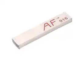
ANT-2.45-CHP-T
Chip Antenna, Ceramic, 2.45 GHz, 6.5mm x 2.2mm x 1mm
⚠️ Reference pricing provided. In case of supply shortages, we will connect you with our trusted procurement partners to ensure your project's continuity.
- Manufacturer: TE CONNECTIVITY - LINX
- Product type: Antennas - Single Band Chip
- SVHC: Lead (21-Jan-2025)
- Product Range: CHP Series
- Centre Frequency: 2.45GHz
- Antenna Case Size: 6.5mm x 2.2mm x 1mm
| Delivery and price | |
|---|---|
| Units per pack | 500 |
| Price | 1.26 € |
| Current stock | 1000+ |
| Lead time | 30 days |
Datasheet

# **Ultra Compact Chip Antenna Data Guide**

## **Table of Contents**

- 1 Description

- 1 Features

- 2 Applications

- 2 Ordering Information

- 2 Electrical Specifications

- 3 Footprints

- 3 Pin Configuration

- 4 Theory of Operation

- 4 Layout Considerations

- 5 Microstrip Details

- 6 Assembly Considerations

- 8 Test Boards

- 9 VSWR Graphs

- 10 Tape Dimensions

- 12 Reel Dimensions

- 13 Mismatch Conversion Table

## **Ultra Compact Chip Antenna Data Guide**

## Description

The exciting ANT-***-CHP family is among the world’s smallest high-performance chip antennas. They are ideal for embedding in wireless products including Bluetooth, 802.11, Home RF, ZigBee and other popular standards. These tiny antennas use advanced Low Temperature Co-fired Ceramic (LTCC) technology and proprietary elements to achieve superior size and performance characteristics. The entire family is compatible with hand and reflow-assembly. Excellent electrical sp ~~e~~ cifications, stability, ~~}~~ and outstandi ~~n~~ g cost-effectiveness make CHP Series antennas the lo ~~g~~ ical choice for a wide variety of applications. ~~;~~

**2.4**

Figure 1: 2.4GHz Dimensions

**xxx** ~~;~~ _A ~~F* 1,~~

## Features

- Incredibly compact SMD package

- Superior LTCC technology

Figure 2: 868MHz and 916MHz Dimensions

- 50 Ω characteristic impedance

- Low loss

- Wide bandwidth

- Favorable linear polarization

- > Unity gain

- No external matching required

- Highly stable over temperature & time

- Hand and reflow-assembly compatible

2.45GHz

LAFin} |___AF ie} 868MHz 916MHz Figure 3: Actual Sizes

- RoHS compliant

- Cost-effective

Revised 8/8/12

– **1** –

## Applications

- Bluetooth

   - Data collection

   - Industrial process monitoring

- 802.11

   - Compact wireless products

- ZigBee

- Wireless PCMCIA cards

   - External antenna elimination

- Telemetry

## Ordering Information

|**Ordering Information**|**Ordering Information**|
|---|---|
|Part Number<br>Description||
|ANT-868-CHP-x|868Mhz Chip Antenna|
|ANT-916-CHP-x|916MHz Chip Antenna|
|ANT-2.45-CHP-x|2.45GHz Chip Antenna|


x = "T" for tape/reel, "B" for bulk

All parts are RoHS compliant. Standard reel is 3,000pcs. (868/916MHz), 1,500pcs. (2.45GHz) Quantities less than reel size are supplied in bulk.

Figure 4: Ordering Information

## Electrical Specifications

|Parameter<br>2.45GHz<br>868MHz<br>916MHz|Parameter<br>2.45GHz<br>868MHz<br>916MHz|Parameter<br>2.45GHz<br>868MHz<br>916MHz|Parameter<br>2.45GHz<br>868MHz<br>916MHz|
|---|---|---|---|
|Physical||||
|Dimensions (mm)|6.5(L) x 2.2(W) x<br>1.0(H)|16.0(L) x 3.0(W) x<br>1.7(H)|16.0(L) x 3.0(W) x<br>1.7(H)|
|Operating/Storage Temp|–40 to +85°C|–40 to +85°C|–40 to +85°C|
|Construction|LTCC|LTCC|LTCC|
|Electrical||||
|Center Frequency|2.45GHz|868MHz|916MHz|
|Bandwidth|180MHz|10MHz|10MHz|
|Wavelength|¼-wave|¼-wave|¼-wave|
|Pattern|Omni-directional|Omni-direction|Omni-directional|
|Polarization|Linear|Linear|Linear|
|VSWR|≤2.0 (Max.)|≤2.0 (Max.)|≤2.0 (Max.)|
|Maximum Gain|+0.5dBi|+0.5dBi|+0.5dBi|
|Impedance|50Ω|50Ω|50Ω|
|Power Handling|3W (Max.)|3W (Max.)|3W (Max.)|


## Footprints

**==> picture [324 x 81] intentionally omitted <==**

**----- Start of picture text -----**<br>
0.260" 0.630"<br>0.100" 0.130"<br>0.040" 0.040"<br>**----- End of picture text -----**<br>


Figure 7: 868MHz and 916MHz Footprint

Figure 6: 2.4GHz Footprint

## Pin Configuration

**==> picture [144 x 37] intentionally omitted <==**

**----- Start of picture text -----**<br>
1 2.4 2<br>**----- End of picture text -----**<br>


Figure 8: Pin Configuration

|||||
|---|---|---|---|
||**Pin Descriptions**|||
||Pin Number|Description||
||1|Feed Termination<br>This pin connects to the transmitter or receiver.||
||2|Solder Termination<br>This pin is soldered down for physical support only. There is no<br>electrical connection.||
|||||


Figure 9: Pin Configurations

Figure 5: Ordering Information

– **2** –

– **3** –

## Theory of Operation

The CHP Series antennas utilize Low Temperature Cofired Ceramic (LTCC) technology to embed the antenna element into a ceramic substrate. Advances in this technology have resulted in materials that are extremely stable over time and temperature, producing an antenna that is highly reliable across a wide range of applications. The high-frequency characteristics of this technology enable exceptional performance in a very small package. The construction techniques for LTCC devices lends itself well to favorable pricing in high volume.

## Layout Considerations

Proper layout is vital to ensure correct operation and optimum performance. Improper placement of planes, traces, or system components will result in nulls or complete de-tuning. Ideally, the antenna will be mounted on the board in such a way as to allow an unobstructed field of view. The area underneath the antenna must be free of components, traces, and planes. Components may be placed to the rear of the antenna in the ground plane counterpoise area. The feed trace from the RF stage to the antenna must be a microstrip trace or coax transmission line and should be kept as short as practical.

The layout of our reference jigs is illustrated on the following pages. While they demonstrate various aspects of a layout, it is not necessary to replicate them exactly. While your board size and layout may differ, it is important to recognize that the counterpoise plays an important role in resonance and stability since it acts, in essence, as part of the antenna. After your own layout is complete, the performance of the antenna in your specific product should be carefully checked using tools like a network analyzer. In some cases, the size of the product’s PCB, proximity of the case, or other factors may make a custom version of the antenna necessary. Contact Linx for more information.

**==> picture [173 x 109] intentionally omitted <==**

**----- Start of picture text -----**<br>
No electrical connection.<br>For physical support only<br>No ground plane or traces<br>under the antenna<br>PCB pads for the CHP<br>Ground plane on bottom<br>layer for counterpoise<br>50-ohm microstrip line<br>2.4<br>**----- End of picture text -----**<br>


Figure 10: Layout

## Microstrip Details

A transmission line is a medium whereby RF energy is transferred from one place to another with minimal loss. This is a critical factor, especially in high-frequency products like Linx RF modules, because the trace leading to the module’s antenna can effectively contribute to the length of the antenna, changing its resonant bandwidth. In order to minimize loss and detuning, some form of transmission line between the antenna and the module should be used unless the antenna can be placed very close (<1/8in.) to the module. One common form of transmission line is a coax cable and another is the microstrip. This term refers to a PCB trace running over a ground plane that is designed to serve as a transmission line between the module and the antenna. The width is based on the desired characteristic impedance of the line, the thickness of the PCB and the dielectric constant of the board material. For standard 0.062in thick FR-4 board material, the trace width would be 111 mils. The correct trace width can be calculated for other widths and materials using the information in Figure 11 and examples are provided in Figure 12. Software for calculating microstrip lines is also available on the Linx website.

**==> picture [221 x 68] intentionally omitted <==**

**----- Start of picture text -----**<br>
Trace<br>Board<br>Ground plane<br>**----- End of picture text -----**<br>


**==> picture [217 x 93] intentionally omitted <==**

Figure 11: Microstrip Formulas

|**Example Microstrip Calculations**<br>Dielectric Constant<br>Width / Height<br>Ratio (W / d)<br>Effective Dielectric<br>Constant<br>Characteristic<br>Impedance (Ω)<br>4.80<br>1.8<br>3.59<br>50.0<br>4.00<br>2.0<br>3.07<br>51.0<br>2.55<br>3.0<br>2.12<br>48.8|**Example Microstrip Calculations**<br>Dielectric Constant<br>Width / Height<br>Ratio (W / d)<br>Effective Dielectric<br>Constant<br>Characteristic<br>Impedance (Ω)<br>4.80<br>1.8<br>3.59<br>50.0<br>4.00<br>2.0<br>3.07<br>51.0<br>2.55<br>3.0<br>2.12<br>48.8|**Example Microstrip Calculations**<br>Dielectric Constant<br>Width / Height<br>Ratio (W / d)<br>Effective Dielectric<br>Constant<br>Characteristic<br>Impedance (Ω)<br>4.80<br>1.8<br>3.59<br>50.0<br>4.00<br>2.0<br>3.07<br>51.0<br>2.55<br>3.0<br>2.12<br>48.8|**Example Microstrip Calculations**<br>Dielectric Constant<br>Width / Height<br>Ratio (W / d)<br>Effective Dielectric<br>Constant<br>Characteristic<br>Impedance (Ω)<br>4.80<br>1.8<br>3.59<br>50.0<br>4.00<br>2.0<br>3.07<br>51.0<br>2.55<br>3.0<br>2.12<br>48.8|**Example Microstrip Calculations**<br>Dielectric Constant<br>Width / Height<br>Ratio (W / d)<br>Effective Dielectric<br>Constant<br>Characteristic<br>Impedance (Ω)<br>4.80<br>1.8<br>3.59<br>50.0<br>4.00<br>2.0<br>3.07<br>51.0<br>2.55<br>3.0<br>2.12<br>48.8|
|---|---|---|---|---|
|4.80||1.8|3.59|50.0|
||4.00|2.0|3.07|51.0|
||2.55|3.0|2.12|48.8|
||||||
||||||


Figure 12: Example Microstrip Calculations

– **4** –

– **5** –

## Assembly Considerations

The antenna is RoHS Compliant and designed to support hand or automated assembly. To avoid damage to the part, the reflow solder guidelines found below should be carefully followed. The antenna is single ended meaning that one pad is electrically connected while the other is for mechanical support only. The antenna terminals are not interchangeable so the polarity indicated in the Pin Configuration section must be observed during assembly.

## Hand Soldering

This antenna is designed for high-volume automated assembly, however, it may be successfully attached by hand assembly techniques. A hand-solder temperature of 225°C or lower should be used. Do not exceed a 10sec. heating time.

## Reflow Temperature Profile

The single most critical stage in the automated assembly process is the reflow process. The reflow profile below should be closely followed since excessive temperatures or transport times during reflow will irreparably damage the antennas. Assembly personnel will need to pay careful attention to the oven's profile to ensure that it meets the requirements necessary to successfully reflow all components while still meeting the limits mandated by the antennas themselves.

## Reflow Soldering Profile

**==> picture [208 x 161] intentionally omitted <==**

**----- Start of picture text -----**<br>
260°C 10 sec, max<br>230°C<br>180°C<br>30 sec.<br>60 sec.<br>Preheating<br>Time (sec.)<br>Temperature (°C)<br>**----- End of picture text -----**<br>


Figure 13: Reflow Soldering Profile

Warning: Pay attention to the absolute maximum solder times.

## **Absolute Maximum Solder Times**

Hand Solder Temperature: TX +225ºC for 10 seconds Hand Solder Temperature: RX +225ºC for 10 seconds Recommended Solder Melting Point: +180ºC Reflow Oven: +225ºC max (see Figure 13)

Figure 14: Absolute Maximum Solder Times

– **6** –

– **7** –

## Test Boards

**==> picture [153 x 145] intentionally omitted <==**

**----- Start of picture text -----**<br>
30<br>20<br>Ground Plane<br>(Top and Bottom Layers)<br>50W Transmission Line<br>30<br>14 14<br>**----- End of picture text -----**<br>


Figure 15. 2.4GHz Test Board 3.30" 0.89" (84mm) (23mm) 0.17" (23mm) 0.08" 1.50" (2mm) **xxx** (38mm) ~~=~~ Figure 16: 868MHz and 916MHz Test Board

## VSWR Graphs

## What is VSWR?

The Voltage Standing Wave Ratio (VSWR) is a measurement of how well an antenna is matched to a source impedance, typically 50-ohms. It is calculated by measuring the voltage wave that is headed toward the load versus the voltage wave that is reflected back from the load. A perfect match will have a VSWR of 1:1. The higher the first number, the worse the match, and the more inefficient the system. Since a perfect match cannot ever be obtained, some benchmark for performance needs to be set. In the case of antenna VSWR, this is usually 2:1. At this point, 88.9% of the energy sent to the antenna by the transmitter is radiated into free space and 11.1% is either reflected back into the source or lost as heat on the structure of the antenna. In the other direction, 88.9% of the energy recovered by the antenna is transferred into the receiver. As a side note, since the “:1” is always implied, many data sheets will remove it and just display the first number.

## How to Read a VSWR Graph

**==> picture [327 x 175] intentionally omitted <==**

**----- Start of picture text -----**<br>
VSWR is usually displayed graphically versus frequency. The lowest point<br>on the graph is the antenna’s operational center frequency. In most cases,<br>this will be different than the designed center frequency due to fabrication<br>tolerances. The VSWR at that point denotes how close to 50-ohms the an-<br>tenna gets. Linx specifies the recommended bandwidth as the range where<br>the typical antenna VSWR is less than 2:1.<br>VSWR 1.681 Reflected Power<br>3:1 . 25%<br>2:1 11%<br>1:1 0%<br>2.4GHz 2.45GHz 2.5GHz<br>**----- End of picture text -----**<br>


Figure 17: 2.4GHz Typical VSWR

**==> picture [255 x 98] intentionally omitted <==**

**----- Start of picture text -----**<br>
VSWR 1.229 Reflected Power<br>3:1 25%<br>2:1 11%<br>1:1 nei 0%<br>818MHz 868MHz 918MHz<br>**----- End of picture text -----**<br>


Figure 18: 868MHz and 916MHz Typical VSWR

– **8** –

– **9** –

## Tape Dimensions

**==> picture [284 x 142] intentionally omitted <==**

**----- Start of picture text -----**<br>
D1 P5 P4 D2<br>T2<br>P3<br>P2<br>W<br>F<br>1.2<br>P1 A0<br>3.1<br>5°<br>T4<br>5°<br>**----- End of picture text -----**<br>


Figure 19: 2.4GHz Tape Dimensions

**2.4GHz Tape Dimensions**

**==> picture [316 x 199] intentionally omitted <==**

**----- Start of picture text -----**<br>
Symbol Dimension Tolerance Unit<br>A0 2.30 ±0.10 mm<br>±0.10<br>D1 1.50 mm<br>–0.00<br>±0.25<br>D2 1.50 mm<br>–0.00<br>F 6.60 ±0.10 mm<br>P1 8.00 ±0.10 mm<br>P2 7.50 ±0.10 mm<br>P3 1.75 ±0.10 mm<br>P4 4.00 ±0.10 mm<br>P5 2.00 ±0.10 mm<br>T2 0.30 ±0.05 mm<br>T4 1.30 ±0.10 mm<br>W 16.00 ±0.10 mm<br>**----- End of picture text -----**<br>


**==> picture [278 x 135] intentionally omitted <==**

**----- Start of picture text -----**<br>
D1 P5 P4 D2 T2<br>P3<br>P2<br>W<br>F<br>P1<br>T4 T3<br>**----- End of picture text -----**<br>


Figure 21: 868MHz and 916MHz Tape Dimensions

**==> picture [324 x 212] intentionally omitted <==**

**----- Start of picture text -----**<br>
868MHz and 916MHz Tape Dimensions<br>Symbol Dimension Tolerance Unit<br>D1 1.50 ±0.10 mm<br>D2 1.50 ±0.10 mm<br>F 10.6 ±0.10 mm<br>P1 8.00 ±0.10 mm<br>P2 11.50 ±0.10 mm<br>P3 1.75 ±0.10 mm<br>P4 4.00 ±0.10 mm<br>P5 2.00 ±0.10 mm<br>T2 0.30 ±0.05 mm<br>T3 3.30 ±0.10 mm<br>T4 1.90 ±0.10 mm<br>W 24.00 ±0.30 mm<br>**----- End of picture text -----**<br>


Figure 21: 868MHz and 916MHz Tape Dimensions Table

Figure 20: 2.4GHz Tape Dimensions Table

– **10** –

– **11** –

## Reel Dimensions

**==> picture [258 x 230] intentionally omitted <==**

**----- Start of picture text -----**<br>
W1<br>E<br>B<br>C<br>A W<br>**----- End of picture text -----**<br>


Figure 22: Reel Dimensions

|QTY per reel|3,000|1,500|pcs|
|---|---|---|---|
|Tape width|24|16|mm|
|A|330±1|180±1|mm|
|B|100±0.5|62±0.5|mm|
|C|13±0.5|13±0.2|mm|
|E|2.2±0.5|2.2±0.5|mm|
|W|24±0.5|16±0.5|mm|
|W1|28.9±0.2|20±0.2|mm|


## Mismatch Conversion Table

**==> picture [324 x 328] intentionally omitted <==**

**----- Start of picture text -----**<br>
Mismatch Conversion Table<br>VSWR Insertion Loss (dB) Power Transmitted (%) Power Reflected (%)<br>17.391 –6.87 20.57% 79.43%<br>11.610 –5.35 29.21% 70.79%<br>8.724 –4.33 36.90% 63.10%<br>6.997 –3.59 43.77% 56.23%<br>5.848 –3.02 49.88% 50.12%<br>5.030 –2.57 55.33% 44.67%<br>4.419 –2.20 60.19% 39.81%<br>3.946 –1.90 64.52% 35.48%<br>3.570 –1.65 68.38% 31.62%<br>3.010 –1.26 74.88% 25.12%<br>2.615 –0.97 80.05% 19.95%<br>2.323 –0.75 84.15% 15.85%<br>2.100 –0.58 87.41% 12.59%<br>1.925 –0.46 90.00% 10.00%<br>1.433 –0.14 96.84% 3.15%<br>1.222 –0.04 99.00% 1.00%<br>1.119 –0.01 99.68% 0.32%<br>1.065 0.00 99.90% 0.10%<br>1.034 0.00 99.97% 0.03%<br>1.020 0.00 99.99% 0.01%<br>**----- End of picture text -----**<br>


Figure 24: Mismatch Conversion Table

Figure 23: Reel Dimensions Table

– **12** –

– **13** –

(This page is intentionally blank.)

(This page is intentionally blank.)

Linx Technologies 159 Ort Lane Merlin, OR, US 97532

3090 Sterling Circle, Suite 200 Boulder, CO 80301

Phone: +1 541 471 6256 Fax: +1 541 471 6251 www.linxtechnologies.com

## Disclaimer

Linx Technologies is continually striving to improve the quality and function of its products. For this reason, we reserve the right to make changes to our products without notice. The information contained in this Data Guide is believed to be accurate as of the time of publication. Specifications are based on representative lot samples. Values may vary from lot-to-lot and are not guaranteed. “Typical” parameters can and do vary over lots and application. Linx Technologies makes no guarantee, warranty, or representation regarding the suitability of any product for use in any specific application. It is Customer’s responsibility to verify the suitability of the part for the intended application. At Customer’s request, Linx Technologies may provide advice and assistance in designing systems and remote control devices that employ Linx Technologies RF products, but responsibility for the ultimate design and use of any such systems and devices remains entirely with Customer and/or user of the RF products.

LINX TECHNOLOGIES DISCLAIMS ANY AND ALL WARRANTIES OF MERCHANTABILITY AND FITNESS FOR A PARTICULAR PURPOSE. IN NO EVENT SHALL LINX TECHNOLOGIES BE LIABLE FOR ANY CUSTOMER’S OR USER’S INCIDENTAL OR CONSEQUENTIAL DAMAGES ARISING OUT OF OR RELATED TO THE DESIGN OR USE OF A REMOTE CONTROL SYSTEM OR DEVICE EMPLOYING LINX TECHNOLOGIES RF PRODUCTS OR FOR ANY OTHER BREACH OF CONTRACT BY LINX TECHNOLOGIES. CUSTOMER AND/OR USER ASSUME ALL RISKS OF DEATH, BODILY INJURIES, OR PROPERTY DAMAGE ARISING OUT OF OR RELATED TO THE USE OF LINX TECHNOLOGIES RF PRODUCTS, INCLUDING WITH RESPECT TO ANY SERVICES PROVIDED BY LINX RELATED TO THE USE OF LINX TECHNOLOGIES RF PRODUCTS. LINX TECHNOLOGIES SHALL NOT BE LIABLE UNDER ANY CIRCUMSTANCES FOR A CUSTOMER’S, USER’S, OR OTHER PERSON’S DEATH, BODILY INJURY, OR PROPERTY DAMAGE ARISING OUT OF OR RELATED TO THE DESIGN OR USE OF A REMOTE CONTROL SYSTEM OR DEVICE EMPLOYING LINX TECHNOLOGIES RF PRODUCTS.

The limitations on Linx Technologies’ liability are applicable to any and all claims or theories of recovery asserted by Customer, including, without limitation, breach of contract, breach of warranty, strict liability, or negligence. Customer assumes all liability (including, without limitation, liability for injury to person or property, economic loss, or business interruption) for all claims, including claims from third parties, arising from the use of the Products. Under no conditions will Linx Technologies be responsible for losses arising from the use or failure of the device in any application, other than the repair, replacement, or refund limited to the original product purchase price. Devices described in this publication may contain proprietary, patented, or copyrighted techniques, components, or materials.

© 2012 Linx Technologies. All rights reserved.

The stylized Linx logo, Wireless Made Simple, CipherLinx, WiSE and the stylized CL logo are trademarks of Linx Technologies.
Updated at April 22, 2026
About Novapart
Novapart is a B2B electronic component broker specialising in stock shortages and cost reduction. We source hard-to-find parts and identify compliant alternatives across a catalogue of 410,000+ components from 500+ manufacturers.
Learn more →Stock Shortage Specialist
When a component is unavailable, discontinued or has an unacceptable lead time, we tap into our network of vetted European and Asian distributors to source what you need — without compromising on quality or traceability.
Request a quote →Compliant Alternatives
We identify pin-to-pin, electrically equivalent substitutes that meet the same certifications (RoHS, AEC-Q100, REACH) as your original specification — validated against datasheets, not just part numbers. Often at a lower cost.
BOM Analysis service →