


AIKW50N65RF5XKSA1
IGBT, 80 A, 1.6 V, 250 W, 650 V, TO-247, 3 Pins
- Manufacturer: INFINEON
- Product type: Single IGBTs
- SVHC: No SVHC (25-Jun-2025)
- No. of Pins: 3Pins
- Product Range: TRENCHSTOP 5 CoolSiC
- Power Dissipation: 250W
- Transistor Mounting: Through Hole
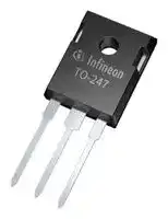
- Transistor Case Style: TO-247
- Operating Temperature Max: 175°C
- Continuous Collector Current: 80A
- Collector Emitter Voltage Max: 650V
- Collector Emitter Saturation Voltage: 1.6V
| Delivery and price | |
|---|---|
| Units per pack | 250 |
| Price | 3.78 € |
| Current stock | 10+ |
| Lead time | 30 days |
## AIKW50N65RF5

**==> picture [223 x 12] intentionally omitted <==**

**----- Start of picture text -----**<br>
CoolSiC™ Hybrid Discrete for  Automotive<br>**----- End of picture text -----**<br>


## Discrete 650V Hybrid with TRENCHSTOP[TM] CoolSiC[TM]

**==> picture [32 x 11] intentionally omitted <==**

**----- Start of picture text -----**<br>
and<br>**----- End of picture text -----**<br>


**==> picture [65 x 10] intentionally omitted <==**

**----- Start of picture text -----**<br>
Applications:<br>**----- End of picture text -----**<br>


**==> picture [375 x 254] intentionally omitted <==**

**----- Start of picture text -----**<br>
C<br>in hard switching and resonant<br>voltage<br>IGBT<br>G<br>Diode G5<br>E<br>G<br>temperature 175°C<br>to AEC-Q101/100<br>ROHS compliant<br>*<br>,<br>=<br>G<br>collector C<br>E<br>**----- End of picture text -----**<br>


|**Type**|**_V_CE**|**_I_C**|**_V_CEsat** **_T_vj=25°C**|**_T_vjmax**|**Marking**|**Package**|
|---|---|---|---|---|---|---|
|AIKW50N65RF5|650V|50A|1.6V|175°C|AK50ERF5|PG-TO247-3|


V 2.5

Datasheet www.infineon.com

2021-02-09

AIKW50N65RF5

**==> picture [86 x 38] intentionally omitted <==**

## CoolSiC™ Hybrid Discrete for Automotive�

## **Table�of�Contents**

Description   . . . . . . . . . . . . . . . . . . . . . . . . . . . . . . . . . . . . . . . . . . . . . . . . . . . . . . . . . . . . . . . . . . . . . . . . 1 Table of Contents   . . . . . . . . . . . . . . . . . . . . . . . . . . . . . . . . . . . . . . . . . . . . . . . . . . . . . . . . . . . . . . . . . . . 2 Maximum Ratings  . . . . . . . . . . . . . . . . . . . . . . . . . . . . . . . . . . . . . . . . . . . . . . . . . . . . . . . . . . . . . . . . . . . 3 Thermal Resistance   . . . . . . . . . . . . . . . . . . . . . . . . . . . . . . . . . . . . . . . . . . . . . . . . . . . . . . . . . . . . . . . . . 3 Electrical Characteristics  . . . . . . . . . . . . . . . . . . . . . . . . . . . . . . . . . . . . . . . . . . . . . . . . . . . . . . . . . . . . . . 4 Electrical Characteristics Diagrams   . . . . . . . . . . . . . . . . . . . . . . . . . . . . . . . . . . . . . . . . . . . . . . . . . . . . . 6 Package Drawing   . . . . . . . . . . . . . . . . . . . . . . . . . . . . . . . . . . . . . . . . . . . . . . . . . . . . . . . . . . . . . . . . . . .11 Testing Conditions   . . . . . . . . . . . . . . . . . . . . . . . . . . . . . . . . . . . . . . . . . . . . . . . . . . . . . . . . . . . . . . . . . .12 Revision History   . . . . . . . . . . . . . . . . . . . . . . . . . . . . . . . . . . . . . . . . . . . . . . . . . . . . . . . . . . . . . . . . . . . .13 Disclaimer  . . . . . . . . . . . . . . . . . . . . . . . . . . . . . . . . . . . . . . . . . . . . . . . . . . . . . . . . . . . . . . . . . . . . . . . . .14

V 2.5 2021-02-09

2

Datasheet

AIKW50N65RF5

**==> picture [86 x 38] intentionally omitted <==**

## CoolSiC™ Hybrid Discrete for Automotive

## **Maximum�Ratings**

|**Parameter**|**Symbol**||**Value**|**Unit**|
|---|---|---|---|---|
|Collector-emitter voltage|_V_CE||650|V|
|DCcollectorcurrent,limitedby_T_vjmax1)<br>_T_c=25°Cvaluelimitedbybondwire<br>_T_c=100°C|_I_C||80.0<br>46.0|A|
|Pulsedcollectorcurrent,_t_plimitedby_T_vjmax1)|_I_Cpuls||150.0|A|
|Turnoffsafeoperatingarea_V_CE≤650V,_T_vj≤175°C1)|-||150.0|A|
|Diodeforwardcurrent,limitedby_T_vjmax1)<br>_T_c=25°Cvaluelimitedbybondwire<br>_T_c=100°C|_I_F||40.0<br>27.0|A|
|Diodepulsedcurrent,_t_plimitedby_T_vjmax1)|_I_Fpuls||100.0|A|
|Gate-emitter voltage1)<br>TransientGate-emittervoltage(_t_p≤10µs,_D_<0.010)|_V_GE||±20<br>±30|V|
|Powerdissipation_T_c=25°C1)<br>Powerdissipation_T_c=100°C|_P_tot||250.0<br>125.0|W|
|Operating junction temperature|_T_vj|-40...+175||°C|
|Storage temperature|_T_stg|-55...+150||°C|
|Soldering temperature,<br>wave soldering1.6mm(0.063in.)from case for 10s|||260|°C|
|Mounting torque, M3 screw<br>Maximum of mounting processes: 3|_M_||0.6|Nm|


## **Thermal�Resistance**

|**ThermalResistance**|||||||
|---|---|---|---|---|---|---|
|**Parameter**|**Symbol **|**Conditions**||**Value**||**Unit**|
||||**min.**|**typ.**|**max.**||
|**RthCharacteristics**|||||||
|IGBT thermal resistance,1)<br>junction - case|_R_th(j-c)||-|0.45|0.60|K/W|
|Diode thermal resistance,1)<br>junction - case|_R_th(j-c)||-|1.00|1.40|K/W|
|Thermal resistance1)<br>junction - ambient|_R_th(j-a)||-|-|40|K/W|


V 2.5 2021-02-09

1) Not subject to production test. Verified by design/characterization

3

Datasheet

AIKW50N65RF5

**==> picture [86 x 38] intentionally omitted <==**

## CoolSiC™ Hybrid Discrete for Automotive

## **Electrical�Characteristic,�at�** _**T**_ **vj�=�25°C,�unless�otherwise�specified**

|**Parameter**|**Symbol **|**Conditions**||**Value**||**Unit**|
|---|---|---|---|---|---|---|
||||**min.**|**typ.**|**max.**||
|**StaticCharacteristic**|||||||
|Collector-emitter breakdown voltage|_V_(BR)CES|_V_GE=0V,_I_C=0.20mA|650|-|-|V|
|Collector-emitter saturation voltage|_V_CEsat|_V_GE=15.0V,_I_C=50.0A<br>_T_vj=25°C<br>_T_vj=125°C<br>_T_vj=175°C|-<br>-<br>-|1.60<br>1.80<br>1.90|2.10<br>-<br>-|V|
|Diode forward voltage|_V_F|_V_GE=0V,_I_F=20.0A<br>_T_vj=25°C<br>_T_vj=125°C<br>_T_vj=175°C|-<br>-<br>-|1.45<br>1.60<br>1.80|1.70<br>-<br>-|V|
|Gate-emitter threshold voltage|_V_GE(th)|_I_C=0.50mA,_V_CE=_V_GE|3.2|4.0|4.8|V|
|Zero gate voltage collector current|_I_CES|_V_CE=650V,_V_GE=0V<br>_T_vj=25°C<br>_T_vj=175°C|-<br>-|-<br>1500|120<br>-|µA|
|Gate-emitter leakage current|_I_GES|_V_CE=0V,_V_GE=20V|-|-|100|nA|
|Transconductance|_g_fs|_V_CE=20V,_I_C=50.0A|-|61.0|-|S|


## **Electrical�Characteristic,�at�** _**T**_ **vj�=�25°C,�unless�otherwise�specified**

|**Parameter**|**Symbol **|**Conditions**||**Value**||**Unit**|
|---|---|---|---|---|---|---|
||||**min.**|**typ.**|**max.**||
|**DynamicCharacteristic**|||||||
|Input capacitance|_C_ies|_V_CE=25V,_V_GE=0V<br>_f_=1000kHz|-|2850|-|pF|
|Output capacitance|_C_oes||-|240|-||
|Reverse transfer capacitance|_C_res||-|8|-||
|Gate charge|_Q_G|_V_CC=520V,_I_C=50.0A,<br>_V_GE=15V|-|109.0|-|nC|
|Internal emitter inductance<br>measured 5mm (0.197 in.) from<br>case|_L_E||-|13.0|-|nH|


## **Switching�Characteristic,�Inductive�Load**

|**Parameter**|**Symbol **|**Conditions**||**Value**||**Unit**|
|---|---|---|---|---|---|---|
||||**min.**|**typ.**|**max.**||
|**IGBTCharacteristic,at****_T_vj=25°C**|||||||
|Turn-on delaytime|_t_d(on)|_T_vj=25°C,<br>_V_CC=400V,_I_C=25.0A,<br>_V_GE=0.0/15.0V,<br>_R_G(on)=12.0Ω,_R_G(off)=12.0Ω,<br>_L_σ=30nH,_C_σ=30pF<br>_L_σ,_C_σfromFig.E<br>Energy losses include “tail” and<br>diode reverse recovery.|-|20|-|ns|
|Rise time|_t_r||-|12|-|ns|
|Turn-off delaytime|_t_d(off)||-|156|-|ns|
|Fall time|_t_f||-|13|-|ns|
|Turn-on energy|_E_on||-|0.31|-|mJ|
|Turn-off energy|_E_off||-|0.12|-|mJ|
|Total switchingenergy|_E_ts||-|0.43|-|mJ|


V 2.5 2021-02-09

Datasheet

4

AIKW50N65RF5

**==> picture [86 x 38] intentionally omitted <==**

## CoolSiC™ Hybrid Discrete for Automotive

|Turn-on delaytime|_t_d(on)|_T_vj=25°C,<br>_V_CC=400V,_I_C=6.0A,<br>_V_GE=0.0/15.0V,<br>_R_G(on)=12.0Ω,_R_G(off)=12.0Ω,<br>_L_σ=30nH,_C_σ=30pF<br>_L_σ,_C_σfromFig.E<br>Energy losses include “tail” and<br>diode reverse recovery.|-|18|-|ns|
|---|---|---|---|---|---|---|
|Rise time|_t_r||-|4|-|ns|
|Turn-off delaytime|_t_d(off)||-|173|-|ns|
|Fall time|_t_f||-|10|-|ns|
|Turn-on energy|_E_on||-|0.07|-|mJ|
|Turn-off energy|_E_off||-|0.04|-|mJ|
|Total switchingenergy|_E_ts||-|0.11|-|mJ|


## **Diode�Characteristic,�at�** _**T**_ **vj�=�25°C**

|Diode reverse recovery charge|_Q_rr|_T_vj=25°C,<br>_V_R=400V,<br>_I_F=25.0A,<br>_di_F_/dt_=200A/µs|-|0.03|-|µC|
|---|---|---|---|---|---|---|


## **Switching�Characteristic,�Inductive�Load**

|**Parameter**|**Symbol **|**Conditions**||**Value**||**Unit**|
|---|---|---|---|---|---|---|
||||**min.**|**typ.**|**max.**||
|**IGBTCharacteristic,at****_T_vj=150°C**|||||||
|Turn-on delaytime|_t_d(on)|_T_vj=150°C,<br>_V_CC=400V,_I_C=25.0A,<br>_V_GE=0.0/15.0V,<br>_R_G(on)=12.0Ω,_R_G(off)=12.0Ω,<br>_L_σ=30nH,_C_σ=30pF<br>_L_σ,_C_σfromFig.E<br>Energy losses include “tail” and<br>diode reverse recovery.|-|20|-|ns|
|Rise time|_t_r||-|15|-|ns|
|Turn-off delaytime|_t_d(off)||-|191|-|ns|
|Fall time|_t_f||-|6|-|ns|
|Turn-on energy|_E_on||-|0.33|-|mJ|
|Turn-off energy|_E_off||-|0.19|-|mJ|
|Total switchingenergy|_E_ts||-|0.52|-|mJ|
||||||||
|Turn-on delaytime|_t_d(on)|_T_vj=150°C,<br>_V_CC=400V,_I_C=6.0A,<br>_V_GE=0.0/15.0V,<br>_R_G(on)=12.0Ω,_R_G(off)=12.0Ω,<br>_L_σ=30nH,_C_σ=30pF<br>_L_σ,_C_σfromFig.E<br>Energy losses include “tail” and<br>diode reverse recovery.|-|17|-|ns|
|Rise time|_t_r||-|6|-|ns|
|Turn-off delaytime|_t_d(off)||-|229|-|ns|
|Fall time|_t_f||-|26|-|ns|
|Turn-on energy|_E_on||-|0.07|-|mJ|
|Turn-off energy|_E_off||-|0.07|-|mJ|
|Total switchingenergy|_E_ts||-|0.14|-|mJ|
|**DiodeCharacteristic,at****_T_vj=150°C**|||||||
|Diode reverse recovery charge1)|_Q_rr|_T_vj=150°C,<br>_V_R=400V,<br>_I_F=25.0A,<br>_di_F_/dt_=200A/µs|-|0.03|-|µC|


1) There is no reverse recovery of Schottky barrier diodes. Qrr denotes capacitive charge Qc.

V 2.5

2021-02-09

Datasheet

5

AIKW50N65RF5

## CoolSiC™ Hybrid Discrete for Automotive

**==> picture [474 x 285] intentionally omitted <==**

**----- Start of picture text -----**<br>
250 90<br>80<br>CT<br>200<br>70<br>60<br>: 7oDNee S CE<br>150<br>50<br>PN<br>40<br>S COON<br>100<br>30<br>Pf Ne<br>fp<br>20<br>50 awN<br>10<br>0 0<br>Pt | tt yA<br>25 50 75 100 125 150 175 25 50 75 100 125 150 175<br>T C , CASE TEMPERATURE [°C] T C , CASE TEMPERATURE [°C]<br>P tot I C<br>**----- End of picture text -----**<br>


> Figure 1. Power **temperature** ( _T_ vj ≤ 175°C)

**==> picture [124 x 28] intentionally omitted <==**

**----- Start of picture text -----**<br>
Figure 2. Collector current as<br>temperature<br>( V GE ≥ 15V, T vj ≤ 175°C)<br>**----- End of picture text -----**<br>


**==> picture [469 x 285] intentionally omitted <==**

**----- Start of picture text -----**<br>
150 150<br>135 VGE = 20V 135<br>18V<br>\ a rive<br>120 120<br> Hee VGE = 20V<br>15V<br>18V<br>105 105<br>12V<br>15V<br>2 | \ ff a a<br>90 10V 90<br>12V<br>8V<br>75 75 10V<br>7V 8V<br>60 60<br>6V 7V<br>45 5V 45 6V<br>5V<br>ie cane: 22<br>30 30<br>15 fy 15<br>D A... | || fk<br>0 0<br>0 1 2 3 4 5 0 1 2 3 4 5<br>V CE , COLLECTOR-EMITTER VOLTAGE [V] V CE , COLLECTOR-EMITTER VOLTAGE [V]<br>I C I C<br>**----- End of picture text -----**<br>


Figure 3. Typical ( _T_ vj=25°C)

Figure 4. Typical ( _T_ vj=150°C)

V 2.5 2021-02-09

6

Datasheet

AIKW50N65RF5

## CoolSiC™ Hybrid Discrete for Automotive

**==> picture [474 x 286] intentionally omitted <==**

**----- Start of picture text -----**<br>
150 2.50<br>140 Tvj = 25°C IC = 12.5A<br>Tvj = 150°C IC = 25A<br>130 ef e 2.25 Ee IC = 50A |i<br>120<br>e e 2.00 P o<br>110<br>-e teiettt t :<br>100<br>eo Pee<br>1.75<br>90<br>ee =<br>80<br>Poo) ee<br>1.50<br>70<br>ee, ee<br>60<br>a / rm 1.25<br>po<br>50<br>9 v7 Se A ee<br>40<br>SE gg 1.00<br>30<br>20 cooppttAL EE © 0.75 [ETT<br>10<br>HPeee CT<br>0 | Tt | 0.50<br>3.5 4.0 4.5 5.0 5.5 6.0 6.5 7.0 7.5 8.0 8.5 9.0 9.5 0 25 50 75 100 125 150 175<br>V GE , GATE-EMITTER VOLTAGE [V] T vj , JUNCTION TEMPERATURE [°C]<br>I C<br>CEsat<br>V<br>**----- End of picture text -----**<br>


Figure 5. Typical ( _V_ CE=20V)

Figure 6.

( _V_ GE=15V)

**==> picture [471 x 344] intentionally omitted <==**

**----- Start of picture text -----**<br>
1000<br>a<br>td(off) td(off)<br>F tf E 1000 tf<br>td(on) td(on)<br>tr tr<br>ee Ee<br>pt P| | | | tt a e<br>>Bee 100 || ii)? Te, e ee<br>n ee a  eeeerr cc aaa se ee P| 100<br>—g fFwa ) —eg aaa| ee<br>= [ylAlt et erteyp 2 ee ee<br>10<br>6 afSe ee A se 10 eTa |<br>ESS<br>pif of fo fof of of ff es<br>1 1<br>0 PECEEEECE) 30 60 90 120 150 |) 5 EEE 15 25 35 45 55 65 75 85<br>I C , COLLECTOR CURRENT [A] r G , GATE RESISTOR [ Ω ]<br>Figure 7. Typical switching times as a function of Figure 8. Typical switching times as a function of<br>collector current resistor<br>(inductive load, T vj =150°C, V CE=400V, (inductive load, T vj =150°C, V CE=400V,<br>V GE =15/0V, r G=12 Ω , Dynamic test circuit in V GE =15/0V, I C =25A,Dynamictest circuit in<br>Datasheet Figure E) 7 Figure E)<br>t t<br>**----- End of picture text -----**<br>


**==> picture [38 x 6] intentionally omitted <==**

**----- Start of picture text -----**<br>
Datasheet<br>**----- End of picture text -----**<br>


V 2.5 2021-02-09

## AIKW50N65RF5

## CoolSiC™ Hybrid Discrete for Automotive

**==> picture [474 x 699] intentionally omitted <==**

**----- Start of picture text -----**<br>
1000 Th arsa Rs 6.0<br>| td(off) a ee ee ee typ.<br>I tf a ee ee eee _ 5.5 min.<br>td(on) max.<br>I a eeee<br>tr<br>| p o WW 5.0<br>rr eee d ~ se<br>4.5<br>100<br>icp) a i ~<br>uw a ee ee (e) 4.0 __— Say<br>= a SO x<br>- a a ~~ oe<br>3.5<br>Oo a Ww- PAL<br><== a — a =<br>O<br>i my 3.0 ~~ ™<br>ee kK ; ~~<br>7 10 pIa e i e ee es Ww 2.5 ~S ~N NS<br>a a a Pe ~X<br>a ee es ee eo) 2.0<br>1.5<br>1 1.0<br>25 50 75 100 125 150 175 0 25 50 75 100 125 150<br>T vj , JUNCTION TEMPERATURE [°C] T vj , JUNCTION TEMPERATURE [°C]<br>Figure 9. Typical switching times as a function of Figure 10. Gate-emitter threshold voltage as a<br>junction temperature of junction temperature<br>(inductive load, V CE =400V, V GE=15/0V, ( I C =0.5mA. Only values at 25°C subject to<br>I C =25A, r G=12 ,Dynamic test circuit in Figure production test. All other values are verified<br>E) by design/characterization)<br>11 Ld 2.50<br>Eoff Eoff<br>10 EEonts / 2.25 EEonts<br>ELOY ELLE<br>/<br>9<br>5 Sa itt tt / 5 2.00 P ri]it tl<br>) 8 f o y<br>uw 0 uw 1.75<br>ip) 7 / ip) ?<br>ep@) Ti iit itl et7 | 3oO “ /<br>1.50<br>ef<br>U)> 6 ¢/La U) v/<br>1.25<br>uw 5 uw ”<br>1.00<br>2 4 foLAa Oo ?<br>Pf} / A de 0.75 > 2<br>= 3 LAY Ye £ go<br>SL 1 q = va if - ~<br>2 OL/ 7 J | 0.50 - < ra -<br>. | Lee<br>1 L727 ———— 0.25 a,a“ —_|<br>0 0.00<br>P22 eeeeee<br>0 30 60 90 120 150 5 15 25 35 45 55 65 75 85<br>I C , COLLECTOR CURRENT [A] r G , GATE RESISTOR [ Ω ]<br>Figure 11. Typical switching energy losses as a Figure 12. Typical switching energy losses as a<br>function of collector current function of gate resistor<br>(inductive load, T vj =150°C, V CE=400V, (inductive load, T vj =150°C, V CE=400V,<br>V GE =15/0V, r G=12 Ω ,Dynamic test circuit in V GE =15/0V, I C =25A, Dynamic test circuit in<br>Figure E) Figure E)<br>t<br>GE(th)<br>V<br>E E<br>**----- End of picture text -----**<br>


**==> picture [38 x 6] intentionally omitted <==**

**----- Start of picture text -----**<br>
Datasheet<br>**----- End of picture text -----**<br>


8

V 2.5 2021-02-09

## AIKW50N65RF5

## CoolSiC™ Hybrid Discrete for Automotive

**==> picture [474 x 679] intentionally omitted <==**

**----- Start of picture text -----**<br>
0.7 0.7<br>Eoff Eoff<br>Eon Eon<br>Ets Ets<br>0.6 0.6<br>£&5 raeye£& | “7 ero”<br>n 0.5 cad n 0.5 cal<br>7) 7) -<br>op) (dp) o<br>i rn oeee<br>a<br>> 0.4 > 0.4 2<br>- ae<br>é o* oa<br>i) oe -e<br>0.3 0.3<br>oO _ WwoO -<br>: 2 |e<br>=<br>O O -<br>0.2 0.2<br>: 4e fee<br>0.1 0.1<br>0.0 0.0<br>25 50 75 100 125 150 175 200 250 300 350 400 450 500<br>T vj , JUNCTION TEMPERATURE [°C] V CE , COLLECTOR-EMITTER VOLTAGE [V]<br>Figure 13. Typical switching energy losses as a Figure 14. Typical switching energy losses as a<br>function of junction temperature function of collector emitter voltage<br>(inductive load, V CE =400V, V GE=15/0V, (inductive load, T vj =150°C, V GE=15/0V,<br>I C =25A, r G=12 ,Dynamic test circuit in I C =25A, r G=12 ,Dynamic test circuit in<br>Figure E) Figure E)<br>16 Lt<br>V CC Cies<br>—— V CC = 520V 7 1E+4 H Coes EEE<br>14 -—— 4, H Cres ee— —<br>a a<br>NT|<br>S 12<br>a<br>1000<br><x / P| | | dT<br>kK— 10 LL._jos poeeaee eeee<br>is: / Z Aa<br>8<br>E Se 100 | a ee<br>= ae oQ e e e<br>L fi zt a<br>Ww 6 oO a<br>Ee - Pp\fT<br>°<br>4<br>10<br>a ss<br>a<br>2 eeee<br>0 1<br>0 20 40 60 80 100 120 0 5 10 15 20 25 30<br>Q GE , GATE CHARGE [nC] V CE , COLLECTOR-EMITTER VOLTAGE [V]<br>Figure 15. Typical gate charge Figure 16. Typical capacitance as a function of<br>( I C=50A) collector-emitter voltage<br>( V GE =0V, f=1MHz)<br>E E<br>C<br>GE<br>V<br>**----- End of picture text -----**<br>


9

V 2.5 2021-02-09

Datasheet

AIKW50N65RF5

## CoolSiC™ Hybrid Discrete for Automotive

**==> picture [495 x 643] intentionally omitted <==**

**----- Start of picture text -----**<br>
1<br>PT TT TT PTT<br>Fett ete Le<br>> ee ae al al _ 1 Se il Feat M I<br>= TL<br>x3 A ICI en =| ES<br>D = 0.5 D = 0.5<br>i eal EAH i eee<br>zm EO ee ain 0.2 a i 0.2<br>BT YA zm er t a<br>0.1 ee 0.1 lll | = C esare 0.1<br>0.05 0.05<br>GFw a 0.1 o mea<br>0.02 0.02<br>z eerT Aa i «= Ee HHe aceee E eea<br>=2 Y | (Uepeeryy [We ju 0.01 S 9 | 0.01 CT Th<br>A |e single pulse TI Sau ERE mo single pulse<br>EBerT ee ey TI gE LUN eA eo Il<br>z= 0.01 sewaad ZzF SeLH rat AA @StTIRUNI<br> tu ul A CITI<br>0.01<br>z LL rani Ry Re z oiAat Ro {iil<br>F AEA TTT cde ole (OF THM CANIACT cae, othe, Il<br>a a maTil 070) TT<br>ya | i: 1 2 | 3 4 CTT ZAC | Lo i: 1 2 3 4<br>ri[K/W]: 0.114077 0.140622 0.204896 0.140406 ri[K/W]: 0.06392 0.50259 0.50688 0.3266<br>τ i[s]: 1.8E-4 1.9E-3 0.019026 0.168313 τ i[s]: 1.0E-4 9.1E-4 6.5E-3 0.0674<br>Ltl a | Zall| a<br>0.001 0.001<br>1E-6 1E-5 1E-4 0.001 0.01 0.1 1 1E-7 1E-6 1E-5 1E-4 0.001 0.01 0.1 1<br>t p , PULSE WIDTH [s] t p , PULSE WIDTH [s]<br>Figure 17. IGBT transient thermal resistance Figure 18. Diode transient thermal impedance as a<br>( D = t p/T) function of pulse width<br>( D = t p/T)<br>80 2.0<br>Tvj = 25°C IF = 12A<br>Tvj = 150°C IF = 20A<br>70<br>ae P| Ed ,<br>1.8<br>60 av st tt] |ty<br>50<br>1.6<br>a / Feera<br>D / O -—<br>6) 40 [ a -<br>rd a -—<br>’<br>s= 1.4<br>: 30<br>, ° oe<br>20<br>1.2<br>10<br>0 AZLLELE)i 1.0<br>0.0 1.0 2.0 3.0 4.0 5.0 6.0 25 50 75 100 125 150 175<br>V F , FORWARD VOLTAGE [V] T vj , JUNCTION TEMPERATURE [°C]<br>c)th(j- c)th(j-<br>Z Z<br>I F V F<br>**----- End of picture text -----**<br>


Figure 19.

Figure 20.

10

V 2.5 2021-02-09

Datasheet

AIKW50N65RF5

**==> picture [86 x 38] intentionally omitted <==**

## CoolSiC™ Hybrid Discrete for Automotiv e�

## **Package Drawing PG-TO247-3**

**==> picture [277 x 417] intentionally omitted <==**

**==> picture [153 x 351] intentionally omitted <==**

**==> picture [300 x 233] intentionally omitted <==**

**----- Start of picture text -----**<br>
MILLIMETERS<br>DIMENSIONS<br>MIN. MAX.<br>A 4.70 5.30<br>A1 2.20 2.60<br>A2 1.50 2.50<br>b 1.00 1.40<br>b1 1.60 2.41 DOCUMENT NO.<br>b2 2.57 3.43 Z8B00003327<br>c 0.38 0.89 REVISION<br>D 20.70 21.50 06<br>D1 13.08 17.65<br>D2 0.51 1.35 SCALE 3:1<br>E 15.50 16.30 0 1 2 3 4 5mm<br>E1 12.38 14.15<br>E2 3.40 5.10<br>E3 1.00 2.60 EUROPEAN PROJECTION<br>e 5.44<br>L 19.80 20.40<br>L1 3.85 4.50<br>P 3.50 3.70<br>Q 5.35 6.25 ISSUE DATE<br>S 6.04 6.30 25.07.2018<br>**----- End of picture text -----**<br>


11

V 2.5 2021-02-09

Datasheet

AIKW50N65RF5

**==> picture [86 x 38] intentionally omitted <==**

## CoolSiC™ Hybrid Discrete for Automotive

## **Testing Conditions**

**==> picture [252 x 588] intentionally omitted <==**

**----- Start of picture text -----**<br>
V GE (t)<br>90%  V GE<br>10%  V GE t<br>I C (t)<br>90%  I C 90%  I C<br>10%  I C 10%  I C<br>t<br>V CE (t)<br>t<br>t d(off) t f t d(on) t r<br>Figure A.<br>V GE (t)<br>90%  V GE<br>10%  V GE<br>t<br>I C (t)<br>2%  I C t<br>V CE (t)<br>t 2 t 4<br>E off  [=] V CE x I C x d t E on  [=] V CE x I C x d t<br>t 1 t 3 2%  V CE<br>t<br>t 1 t 2 t 3 t 4<br>Figure B.<br>**----- End of picture text -----**<br>


**==> picture [189 x 170] intentionally omitted <==**

**----- Start of picture text -----**<br>
I,V<br>dI F /dt Qt rrrr== Qt aa++ tQ b b<br>a b<br>Q a Q b<br>dI<br>Figure C.  Definition of diode switching<br>characteristics<br>**----- End of picture text -----**<br>


**==> picture [7 x 7] intentionally omitted <==**

**----- Start of picture text -----**<br>
t<br>**----- End of picture text -----**<br>


**==> picture [169 x 63] intentionally omitted <==**

Figure D.

**==> picture [7 x 4] intentionally omitted <==**

**----- Start of picture text -----**<br>
CC<br>**----- End of picture text -----**<br>


Figure E. **Dynamic test circuit** Parasitic inductance Ls, parasitic capacitor Cs, relief capacitor C ,r (only for ZVT switching)

12

V 2.5 2021-02-09

Datasheet

AIKW50N65RF5

**==> picture [86 x 38] intentionally omitted <==**

## CoolSiC™ Hybrid Discrete for Automotive

## **Revision�History**

## AIKW50N65RF5

## **Revision:�202 1 - 02-09 ,�Rev.�2. 5**

## Previous Revision

|Revision|Revision|Date|Date|Subjects(major changes since last revision)|Subjects(major changes since last revision)|
|---|---|---|---|---|---|
|2.1||2020-02-27||Final Data Sheet||
|2.2||2020-03-03||Disclaimer changed to Automotive.||
|2.3||2020-09-17||Update figure 15 typicalgate charge||
|2.4||2020-12-03||Open market branding||
|2.5||2021-02-09||Updateproduct familyname to CoolSiC™Hybrid Discrete||


13

V 2.5 2021-02-09

Datasheet

## **Trademarks**

**==> picture [9 x 8] intentionally omitted <==**

## party.

## **Warnings**
Updated at June 9, 2026
Infineon Technologies is a globally recognized leader in semiconductor solutions, renowned for driving innovation in power management, energy efficiency, and modern mobility. With a strong legacy of engineering excellence, the company provides highly reliable components designed to meet the rigorous demands of industrial, automotive, and advanced commercial applications. The core of our Infineon portfolio is centered on their industry-leading discrete semiconductors. We offer an extensive selection of single and dual MOSFETs, alongside a robust range of single IGBTs and advanced IGBT modules. These flagship power transistors are essential for high-efficiency power conversion and motor control, providing engineers with superior thermal performance and minimized switching losses. Beyond advanced field-effect transistors, the selection includes a comprehensive array of diodes and rectifiers, heavily featuring Schottky diodes, as well as fast-recovery and RF/PIN diodes. This power foundation is further supported by bipolar transistors, intelligent power modules, and thyristor SCR modules, delivering the critical building blocks required for complex power system designs. To support broader system integration, the portfolio also encompasses specialized solutions such as solid-state relays, AC/DC LED driver ICs, and Bluetooth communications modules. From high-power industrial rectifiers to wireless connectivity adapters, Infineon equips designers with the precision components needed to build efficient, scalable, and fully connected electronic systems.
About Novapart
Novapart is a B2B electronic component broker specialising in stock shortages and cost reduction. We source hard-to-find parts and identify compliant alternatives across a catalogue of 410,000+ components from 500+ manufacturers.
Learn more →Stock Shortage Specialist
When a component is unavailable, discontinued or has an unacceptable lead time, we tap into our network of vetted European and Asian distributors to source what you need — without compromising on quality or traceability.
Request a quote →Compliant Alternatives
We identify pin-to-pin, electrically equivalent substitutes that meet the same certifications (RoHS, AEC-Q100, REACH) as your original specification — validated against datasheets, not just part numbers. Often at a lower cost.
BOM Analysis service →