


AIKW40N65DH5XKSA1
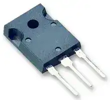
IGBT, 74 A, 1.66 V, 250 W, 650 V, TO-247, 3 Pins
- Manufacturer: INFINEON
- Product type: Single IGBTs
- DC Collector Current:74A; Collector Emitter Saturation Voltage Vce(on):1.66V; Power Dissipation Pd:250W; Collector Emitter Voltage V(br)ceo:650V; Transistor Case Style:TO-247; No.
- MSL: MSL 1 - Unlimited
- SVHC: No SVHC (25-Jun-2025)
- No. of Pins: 3Pins
- Product Range: TRENCHSTOP 5
- Power Dissipation: 250W
- Transistor Mounting: Through Hole
- Transistor Case Style: TO-247
- Operating Temperature Max: 175°C
- Continuous Collector Current: 74A
- Collector Emitter Voltage Max: 650V
- Collector Emitter Saturation Voltage: 1.66V
| Delivery and price | |
|---|---|
| Units per pack | 1000 |
| Price | 2.37 € |
| Current stock | 10+ |
| Lead time | 30 days |
## AIKW40N65DH5

**==> picture [468 x 300] intentionally omitted <==**

**----- Start of picture text -----**<br>
High speed fast IGBT in TRENCHSTOP _ TM 5 technology copacked with<br>RAPID 1 fast and soft antiparallel diode<br>Features and Benefits: C<br>High speed H5 technology offering:<br>Best-in-Class efficiency in hard switching and resonant<br>topologies<br>Plug and play replacement of previous generation IGBTs<br>G<br>650V breakdown voltage<br>E<br>Low gate charge Q G<br>IGBT copacked with RAPID 1 fast and soft antiparallel diode<br>Maximum junction temperature 175°C<br>Dynamically stress tested<br>Qualified according to AEC-Q101 =<br>Green package (ROHS compliant) Gy,<br>Complete product spectrum and PSpice Models: re liteg,<br>http://www. infineon.com/igbt/ i aa<br>Applications:<br>Off-board charger<br>On-board charger<br>DC/DC converter 1<br>Power-Factor correction 2<br>3<br>**----- End of picture text -----**<br>


**==> picture [65 x 10] intentionally omitted <==**

**----- Start of picture text -----**<br>
Applications:<br>**----- End of picture text -----**<br>


|**Type**|**_V_CE**|**_I_C**|**_V_CEsat** **_T_vj=25°C**|**_T_vjmax**|**Marking**|**Package**|
|---|---|---|---|---|---|---|
|AIKW40N65DH5|650V|40A|1.66V|175°C|AK40EDH5|PG-TO247-3|


Datasheet www.infineon.com

2017-06-30

AIKW40N65DH5

**==> picture [86 x 38] intentionally omitted <==**

## High�speed�switching�series�fifth�generation

## **Table�of�Contents**

Description   . . . . . . . . . . . . . . . . . . . . . . . . . . . . . . . . . . . . . . . . . . . . . . . . . . . . . . . . . . . . . . . . . . . . . . . . 1 Table of Contents   . . . . . . . . . . . . . . . . . . . . . . . . . . . . . . . . . . . . . . . . . . . . . . . . . . . . . . . . . . . . . . . . . . . 2 Maximum Ratings  . . . . . . . . . . . . . . . . . . . . . . . . . . . . . . . . . . . . . . . . . . . . . . . . . . . . . . . . . . . . . . . . . . . 3 Thermal Resistance   . . . . . . . . . . . . . . . . . . . . . . . . . . . . . . . . . . . . . . . . . . . . . . . . . . . . . . . . . . . . . . . . . 3 Electrical Characteristics  . . . . . . . . . . . . . . . . . . . . . . . . . . . . . . . . . . . . . . . . . . . . . . . . . . . . . . . . . . . . . . 4 Electrical Characteristics Diagrams   . . . . . . . . . . . . . . . . . . . . . . . . . . . . . . . . . . . . . . . . . . . . . . . . . . . . . 7 Package Drawing   . . . . . . . . . . . . . . . . . . . . . . . . . . . . . . . . . . . . . . . . . . . . . . . . . . . . . . . . . . . . . . . . . . .13 Testing Conditions   . . . . . . . . . . . . . . . . . . . . . . . . . . . . . . . . . . . . . . . . . . . . . . . . . . . . . . . . . . . . . . . . . .14 Revision History   . . . . . . . . . . . . . . . . . . . . . . . . . . . . . . . . . . . . . . . . . . . . . . . . . . . . . . . . . . . . . . . . . . . .15 Disclaimer  . . . . . . . . . . . . . . . . . . . . . . . . . . . . . . . . . . . . . . . . . . . . . . . . . . . . . . . . . . . . . . . . . . . . . . . . .16

2

V�2.1 2017-06-30

Datasheet

AIKW40N65DH5

**==> picture [86 x 38] intentionally omitted <==**

## High�speed�switching�series�fifth�generation

## **Maximum�Ratings**

|**Parameter**|**Symbol**||**Value**|**Unit**|
|---|---|---|---|---|
|Collector-emittervoltage,_T_vj≥25°C|_V_CE||650|V|
|DCcollectorcurrent,limitedby_T_vjmax<br>_T_C=25°C<br>_T_C=100°C|_I_C||74.0<br>46.0|A|
|Pulsedcollectorcurrent,_t_plimitedby_T_vjmax1)|_I_Cpuls||120.0|A|
|Turn off safe operating area<br>_V_CE≤650V,_T_vj≤175°C,_t_p=1µs1)|-||120.0|A|
|Diodeforwardcurrent,limitedby_T_vjmax<br>_T_C=25°C<br>_T_C=100°C|_I_F||36.0<br>21.0|A|
|Diodepulsedcurrent,_t_plimitedby_T_vjmax1)|_I_Fpuls||120.0|A|
|Gate-emitter voltage<br>TransientGate-emittervoltage(_t_p≤10µs,_D_<0.010)|_V_GE||±20<br>±30|V|
|Powerdissipation_T_C=25°C<br>Powerdissipation_T_C=100°C|_P_tot||250.0<br>125.0|W|
|Operating junction temperature|_T_vj|-40...+175||°C|
|Storage temperature|_T_stg|-55...+150||°C|
|Soldering temperature,2)<br>wave soldering1.6mm(0.063in.)from case for 10s|||260|°C|
|Mounting torque, M3 screw<br>Maximum of mounting processes: 3|_M_||0.6|Nm|


## **Thermal�Resistance**

|**ThermalResistance**|||||||
|---|---|---|---|---|---|---|
|**Parameter**|**Symbol **|**Conditions**||**Value**||**Unit**|
||||**min.**|**typ.**|**max.**||
|**RthCharacteristics**|||||||
|IGBT thermal resistance,<br>junction - case|_R_th(j-C)||-|-|0.60|K/W|
|Diode thermal resistance,<br>junction - case|_R_th(j-C)||-|-|1.80|K/W|
|Thermal resistance<br>junction - ambient|_R_th(j-a)||-|-|40|K/W|


1) Defined by design. Not subject to production test.

2) Package not recommended for surface mount applications.

3

V�2.1 2017-06-30

Datasheet

AIKW40N65DH5

**==> picture [86 x 38] intentionally omitted <==**

## High�speed�switching�series�fifth�generation

## **Electrical�Characteristic,�at�** _**T**_ **vj�=�25°C,�unless�otherwise�specified**

|**Parameter**|**Symbol **|**Conditions**||**Value**||**Unit**|
|---|---|---|---|---|---|---|
||||**min.**|**typ.**|**max.**||
|**StaticCharacteristic**|||||||
|Collector-emitter breakdown voltage|_V_(BR)CES|_V_GE=0V,_I_C=0.20mA|650|-|-|V|
|Collector-emitter saturation voltage|_V_CEsat|_V_GE=15.0V,_I_C=40.0A<br>_T_vj=25°C<br>_T_vj=125°C<br>_T_vj=175°C|-<br>-<br>-|1.66<br>1.85<br>2.05|2.10<br>-<br>-|V|
|Diode forward voltage|_V_F|_V_GE=0V,_I_F=20.0A<br>_T_vj=25°C<br>_T_vj=125°C<br>_T_vj=175°C|-<br>-<br>-|1.55<br>1.53<br>1.49|1.80<br>-<br>-|V|
|Gate-emitter threshold voltage|_V_GE(th)|_I_C=0.40mA,_V_CE=_V_GE|3.2|4.0|4.8|V|
|Zero gate voltage collector current|_I_CES|_V_CE=650V,_V_GE=0V<br>_T_vj=25°C<br>_T_vj=175°C|-<br>-|-<br>800|40<br>-|µA|
|Gate-emitter leakage current|_I_GES|_V_CE=0V,_V_GE=20V|-|-|100|nA|
|Transconductance|_g_fs|_V_CE=20V,_I_C=40.0A|-|50.0|-|S|


## **Electrical�Characteristic,�at�** _**T**_ **vj�=�25°C,�unless�otherwise�specified**

|**Parameter**|**Symbol **|**Conditions**||**Value**||**Unit**|
|---|---|---|---|---|---|---|
||||**min.**|**typ.**|**max.**||
|**DynamicCharacteristic**|||||||
|Input capacitance|_C_ies|_V_CE=25V,_V_GE=0V,f=1MHz|-|2300|-|pF|
|Output capacitance|_C_oes||-|43|-||
|Reverse transfer capacitance|_C_res||-|9|-||
|Gate charge|_Q_G|_V_CC=520V,_I_C=40.0A,<br>_V_GE=15V|-|92.0|-|nC|
|Internal emitter inductance<br>measured 5mm (0.197 in.) from<br>case|_L_E||-|13.0|-|nH|


## **Switching�Characteristic,�Inductive�Load**

|**Parameter**|**Symbol **|**Conditions**||**Value**||**Unit**|
|---|---|---|---|---|---|---|
||||**min.**|**typ.**|**max.**||
|**IGBTCharacteristic,at****_T_vj=25°C**|||||||
|Turn-on delaytime|_t_d(on)|_T_vj=25°C,<br>_V_CC=400V,_I_C=20.0A,<br>_V_GE=0.0/15.0V,<br>_R_G(on)=15.0Ω,_R_G(off)=15.0Ω,<br>_L_σ=30nH,_C_σ=30pF<br>_L_σ,_C_σfromFig.E<br>Energy losses include “tail” and<br>diode reverse recovery.|-|20|-|ns|
|Rise time|_t_r||-|11|-|ns|
|Turn-off delaytime|_t_d(off)||-|153|-|ns|
|Fall time|_t_f||-|11|-|ns|
|Turn-on energy|_E_on||-|0.38|-|mJ|
|Turn-off energy|_E_off||-|0.12|-|mJ|
|Total switchingenergy|_E_ts||-|0.50|-|mJ|


V�2.1 2017-06-30

Datasheet

4

AIKW40N65DH5

**==> picture [86 x 38] intentionally omitted <==**

## High�speed�switching�series�fifth�generation

|Turn-on delaytime|_t_d(on)|_T_vj=25°C,<br>_V_CC=400V,_I_C=5.0A,<br>_V_GE=0.0/15.0V,<br>_R_G(on)=15.0Ω,_R_G(off)=15.0Ω,<br>_L_σ=30nH,_C_σ=30pF<br>_L_σ,_C_σfromFig.E<br>Energy losses include “tail” and<br>diode reverse recovery.|-|18|-|ns|
|---|---|---|---|---|---|---|
|Rise time|_t_r||-|4|-|ns|
|Turn-off delaytime|_t_d(off)||-|161|-|ns|
|Fall time|_t_f||-|24|-|ns|
|Turn-on energy|_E_on||-|0.08|-|mJ|
|Turn-off energy|_E_off||-|0.04|-|mJ|
|Total switchingenergy|_E_ts||-|0.12|-|mJ|
|**DiodeCharacteristic,at****_T_vj=25°C**|||||||
|Diode reverse recoverytime|_t_rr|_T_vj=25°C,<br>_V_R=400V,<br>_I_F=20.0A,<br>_di_F_/dt_=1000A/µs|-|75|-|ns|
|Diode reverse recoverycharge|_Q_rr||-|0.52|-|µC|
|Diodepeak reverse recoverycurrent|_I_rrm||-|13.1|-|A|
|Diode peak rate of fall of reverse<br>recoverycurrentduring_t_b|_di_rr_/dt_||-|-217|-|A/µs|
||||||||
|Diode reverse recoverytime|_t_rr|_T_vj=25°C,<br>_V_R=400V,<br>_I_F=5.0A,<br>_di_F_/dt_=1000A/µs|-|37|-|ns|
|Diode reverse recoverycharge|_Q_rr||-|0.23|-|µC|
|Diodepeak reverse recoverycurrent|_I_rrm||-|10.2|-|A|
|Diode peak rate of fall of reverse<br>recoverycurrentduring_t_b|_di_rr_/dt_||-|-550|-|A/µs|


## **Switching�Characteristic,�Inductive�Load**

|**Parameter**|**Symbol **|**Conditions**||**Value**||**Unit**|
|---|---|---|---|---|---|---|
||||**min.**|**typ.**|**max.**||
|**IGBTCharacteristic,at****_T_vj=150°C**|||||||
|Turn-on delaytime|_t_d(on)|_T_vj=150°C,<br>_V_CC=400V,_I_C=20.0A,<br>_V_GE=0.0/15.0V,<br>_R_G(on)=15.0Ω,_R_G(off)=15.0Ω,<br>_L_σ=30nH,_C_σ=30pF<br>_L_σ,_C_σfromFig.E<br>Energy losses include “tail” and<br>diode reverse recovery.|-|20|-|ns|
|Rise time|_t_r||-|12|-|ns|
|Turn-off delaytime|_t_d(off)||-|190|-|ns|
|Fall time|_t_f||-|14|-|ns|
|Turn-on energy|_E_on||-|0.57|-|mJ|
|Turn-off energy|_E_off||-|0.22|-|mJ|
|Total switchingenergy|_E_ts||-|0.79|-|mJ|
||||||||
|Turn-on delaytime|_t_d(on)|_T_vj=150°C,<br>_V_CC=400V,_I_C=5.0A,<br>_V_GE=0.0/15.0V,<br>_R_G(on)=15.0Ω,_R_G(off)=15.0Ω,<br>_L_σ=30nH,_C_σ=30pF<br>_L_σ,_C_σfromFig.E<br>Energy losses include “tail” and<br>diode reverse recovery.|-|17|-|ns|
|Rise time|_t_r||-|4|-|ns|
|Turn-off delaytime|_t_d(off)||-|223|-|ns|
|Fall time|_t_f||-|25|-|ns|
|Turn-on energy|_E_on||-|0.16|-|mJ|
|Turn-off energy|_E_off||-|0.06|-|mJ|
|Total switchingenergy|_E_ts||-|0.22|-|mJ|


V�2.1 2017-06-30

Datasheet

5

AIKW40N65DH5

**==> picture [86 x 38] intentionally omitted <==**

## High�speed�switching�series�fifth�generation

**Diode�Characteristic,�at�** _**T**_ **vj�=�150°C**

|Diode reverse recoverytime|_t_rr|_T_vj=150°C,<br>_V_R=400V,<br>_I_F=20.0A,<br>_di_F_/dt_=1000A/µs|-|128|-|ns|
|---|---|---|---|---|---|---|
|Diode reverse recoverycharge|_Q_rr||-|1.22|-|µC|
|Diodepeak reverse recoverycurrent|_I_rrm||-|18.6|-|A|
|Diode peak rate of fall of reverse<br>recoverycurrentduring_t_b|_di_rr_/dt_||-|-170|-|A/µs|
||||||||
|Diode reverse recoverytime|_t_rr|_T_vj=150°C,<br>_V_R=400V,<br>_I_F=5.0A,<br>_di_F_/dt_=1000A/µs|-|68|-|ns|
|Diode reverse recoverycharge|_Q_rr||-|0.58|-|µC|
|Diodepeak reverse recoverycurrent|_I_rrm||-|15.5|-|A|
|Diode peak rate of fall of reverse<br>recoverycurrentduring_t_b|_di_rr_/dt_||-|-320|-|A/µs|


6

V�2.1 2017-06-30

Datasheet

AIKW40N65DH5

**==> picture [474 x 670] intentionally omitted <==**

**----- Start of picture text -----**<br>
275 80<br>250<br>TTTTTT] 70 Ty] [Td<br>225<br>CEE, 60 IA<br>200<br>- AEE. PA<br>ae ee 175 50<br>150<br>pho KBP DN<br>40<br>125<br>ee 100 30 |<br>er 75 TNC ye fr KA<br>20<br>50<br>Ne ee<br>10<br>ee \<br>25<br>0 Sg 0<br>25 50 75 100 125 150 175 25 50 75 100 125 150 175<br>T C , CASE TEMPERATURE [°C] T C , CASE TEMPERATURE [°C]<br>Figure 1. Power dissipation as a function of case Figure 2. Collector current as a function of case<br>temperature temperature<br>( T vj ≤ 175°C) ( V GE ≥ 15V, T vj ≤ 175°C)<br>120 120<br>To Ae<br>100 100<br>COA C7<br>VGE = 20V VGE = 20V<br>a Ca<br>18V 18V<br>80 80<br>ea 15V 15V<br>7an7s 12V ea |e Lee 12V<br>8 60 10V iVaneen 60 ene) 10V //ae a e<br>LOW ce<br>8V 8V<br>BC eae ee<br>7V 7V<br>40 40<br>ees 6V /Geeeees eeen8 6V (4p —<br>S NPR 5V & Re 5V<br>20 20<br>PON) PNK<br>PORK EE) EO JRBS<br>0 ZS 0 O EAEN<br>0 1 2 3 4 5 0 1 2 3 4 5<br>V CE , COLLECTOR-EMITTER VOLTAGE [V] V CE , COLLECTOR-EMITTER VOLTAGE [V]<br>Figure 3. Typical output characteristic Figure 4. Typical output characteristic<br>( T vj=25°C) ( T vj=150°C)<br>P tot I C<br>I C I C<br>**----- End of picture text -----**<br>


Datasheet

7

2017-06-30

## AIKW40N65DH5

**==> picture [236 x 313] intentionally omitted <==**

**----- Start of picture text -----**<br>
120<br>Tj = 25°C<br>E Tj = 150°C y<br>100 aa | yyIf5 |<br>p L|<br>ee<br>80<br>Pa ee<br>Ww<br>ee<br>rs)w 60 /|<br>Ww<br>=e ed<br>(oe) 40 ['<br>.<br>2 A 7<br>CCT<br>20 Pt [TY] 7 | |<br>0 — ———|<br>cet—_— 7 trrr )<br>4.5 5.0 5.5 6.0 6.5 7.0 7.5 8.0 8.5<br>V GE , GATE-EMITTER VOLTAGE [V]<br>Figure 5. Typical transfer characteristic<br>( V CE=20V)<br>I C<br>**----- End of picture text -----**<br>


**==> picture [233 x 286] intentionally omitted <==**

**----- Start of picture text -----**<br>
2.50<br>IC = 5A<br>IC = 10A<br>2.25 IC = 20A<br>IC = 40A Ree<br>s<br>z 2.00<br>=<br>ll<br>rE<br><x 1.75<br>ee:<br>EE 1.50<br>ad<br>1.25<br>_<br>® 1.00<br>0.75<br>0.50<br>Liltt dt<br>0 25 50 75 100 125 150 175<br>T vj , JUNCTION TEMPERATURE [°C]<br>CEsat<br>V<br>**----- End of picture text -----**<br>


Figure 6. Typical a function ( _V_ GE=15V)

**==> picture [471 x 342] intentionally omitted <==**

**----- Start of picture text -----**<br>
1000 a a 1000 a SS SS ES ES<br>1| td(off) a ee ee ee | td(off) se ee ee ae<br>I tf p a a o i| tf aa aee eeeteee eee<br>td(on) td(on)<br>tr tr<br>F he FE be<br>| p o | Pea eee<br>= + } | {| _}<br>5 |<br>— 100 ee cs 100 a<br>ip) a a es<br>uw aa aeeenee ee ip)<br>= ce | a a<br>- a ee ee ee = a eeeee<br>Q eea es eeaae ee ee” a ee e eeeee<br>ef ete] eer |<br>= a = in eo ae<br>2)- 10 aa a ee 2)- 10 Aa SS<br>po a es ss es<br>a<br>aa ee ee aeeee ee<br>ee es a Deee<br>a Pf ft | hc] |<br>1 1<br>0 20 40 60 80 100 120 5 15 25 35 45 55 65 75 85<br>I C , COLLECTOR CURRENT [A] r G , GATE RESISTOR [ Ω ]<br>Figure 7. Typical switching times as a function of Figure 8. Typical switching times as a function of<br>collector current resistor<br>(inductive load, T vj =150°C, V CE=400V, (inductive load, T vj =150°C, V CE=400V,<br>V GE =15/0V, r G=15 Ω , Dynamic test circuit in V GE =15/0V, I C =20A,Dynamic test circuit in<br>Figure E) Figure E)<br>t t<br>**----- End of picture text -----**<br>


8

Datasheet

2017-06-30

AIKW40N65DH5

**==> picture [474 x 699] intentionally omitted <==**

**----- Start of picture text -----**<br>
1000 aEs |1 td(off) a aaRs  ee a a ee ee 5.5 typ.<br>tf min.<br>I td(on) aee 5.0 a max.<br>tr<br><x<br>rr — FE 4.5 S<br>=2 100 —Fryry fT aaye 4.0 hbKA | ~~ SN<br>ip)im= po a aes a (e)a ae SAY aw ~N.<br>- a a 3.5 Pe ~<br>es ee Ww a<br><= - ~<br>3.0<br>= | | | ed og AR —?<br>e _ — Lu ~ ~~<br>= pees eee ecteloeeee- ee meee La ~<br>10 2.5<br>7 a 7 Nn<br>po wi<br>ee N<br>a eseo) 2.0 ]<br>1.5<br>1 1.0<br>25 50 75 100 125 150 175 0 25 50 75 100 125 150<br>T vj , JUNCTION TEMPERATURE [°C] T vj , JUNCTION TEMPERATURE [°C]<br>Figure 9. Typical switching times as a function of Figure 10. Gate-emitter threshold voltage as a<br>junction temperature of junction temperature<br>(inductive load, V CE =400V, V GE=15/0V, ( I C=0.4mA)<br>I C =20A, r G=15 ,Dynamic test circuit in Figure<br>E)<br>8 1.6<br>Eoff Eoff<br>Eon y/ Eon aa<br>7 = Ets / / 1.4 = Ets Y<br>/ 7<br>‘<br>_ / _ “<br>6 1.2<br>Lu / Lu “<br>io) / ip) y<br>(op) / (op) 7 -<br>e) 5 f e) 1.0 <<br>> / vA > “ =<br>©) / yo ©) 4A a7<br>w / iad Pa a<br>WwW 4 Ww 0.8 L<br>Zz / 7 Zz y a<br>Lu / WA Lu a -<br>Oo / / Oo a<br>Zz 3 Zz 0.6<br>: Awa : -<br>== 2 /aa yZO == 0.4 a ma<br>fa 1 / 7 a 0.2 LL|| | —<br>as<br>0 0.0<br>0 20 40 60 80 100 120 5 15 25 35 45 55 65 75 85<br>I C , COLLECTOR CURRENT [A] r G , GATE RESISTOR [ Ω ]<br>Figure 11. Typical switching energy losses as a Figure 12. Typical switching energy losses as a<br>function of collector current function of gate resistor<br>(inductive load, T vj =150°C, V CE=400V, (inductive load, T vj =150°C, V CE=400V,<br>V GE =15/0V, r G=15 Ω ,Dynamic test circuit in V GE =15/0V, I C =20A, Dynamic test circuit in<br>Figure E) Figure E)<br>t<br>GE(th)<br>V<br>E E<br>**----- End of picture text -----**<br>


9

Datasheet

2017-06-30

AIKW40N65DH5

**==> picture [474 x 342] intentionally omitted <==**

**----- Start of picture text -----**<br>
0.9 1.0<br>Eoff Eoff<br>0.8 EEonts oa 0.9 EEonts 7<br>El l lt l4 ELEL Ee<br>en 0.7 ee ee 0.8 ee<br>“oO “7 “ op) 0.7 ve<br>0.6<br>0.6<br>> oT _ > “ Za<br>0.5<br>0.5<br>0.4<br>oO oO 0.4<br>0.3<br>E 0.3<br>;<br>0)<br>0.2<br>0.2<br>0) ee |<br>0.1 eee ee 0.1 ee<br>0.0 0.0<br>25 50 75 100 125 150 175 200 250 300 350 400 450 500<br>T vj , JUNCTION TEMPERATURE [°C] V CE , COLLECTOR-EMITTER VOLTAGE [V]<br>Figure 13. Typical switching energy losses as a Figure 14. Typical switching energy losses as a<br>function of junction temperature function of collector emitter voltage<br>(inductive load, V CE =400V, V GE=15/0V, (inductive load, T vj =150°C, V GE=15/0V,<br>I C =20A, r G=15 ,Dynamic test circuit in I C =20A, r G=15 ,Dynamic test circuit in<br>Figure E) Figure E)<br>E E<br>**----- End of picture text -----**<br>


**==> picture [471 x 322] intentionally omitted <==**

**----- Start of picture text -----**<br>
16 1E+4<br>— V CC = 130V H Cies ee<br>V CC Coes<br>14 —-  =520V L (,/ i\ Cres pa o a<br>5 12 1000 |<br>oO —_ a ee<br><x LL Ps<br>FE 10 A 2 (a<br>e woo<br>LL 8 i 100 a ee ee ee<br>E ff 7 ————<br>= o ee<br>i ip a a ee<br>Lu 6 Oo aee<br>* 4 10 i eee<br>a es ss ee<br>po<br>2 a es<br>0 1<br>0 20 40 60 80 100 0 5 10 15 20 25 30<br>Q GE , GATE CHARGE [nC] V CE , COLLECTOR-EMITTER VOLTAGE [V]<br>Figure 15. Typical gate charge Figure 16. Typical capacitance as a function of<br>( I C=40A) collector-emitter voltage<br>( V GE =0V, f=1MHZz)<br>C<br>GE<br>V<br>**----- End of picture text -----**<br>


10

Datasheet

2017-06-30

AIKW40N65DH5

**==> picture [476 x 313] intentionally omitted <==**

**----- Start of picture text -----**<br>
1<br>TTT AT 1 Pall imilil<br>s FOIAeee rll SSS eA ay<br>S ceo Pei Lf<br>Tr De D = 0.5 5 eV D = 0.5<br>TTT TTI ae allem ee ee<br>0.2 0.2<br>gem) 0.1 = Ua 0.1<br>a 0.1 on | Ba! a |} Tit Pe<br>ul eee 0.05 ey 0.1 aa a ye 0.05<br>= ae oS eee ee aieseetl<br>z5 Teorn ee 0.02 TC)oo eeCeCeAV 0.02<br>rd= pert| ee ae pu 0.01 S | 0.01 CT Th<br>uw= TVANI TT single pulse colL lll)Ie ertSenerZIMau ENEer TTso single pulse Mill<br>F ga tt I a x pina y<br>2 0.01 geeA TT TTI tC ST LEAH<br>QD Pecoed z 0.01 ON NAY)<br>J Ri Ro Aa | Ri Ro tt}<br>- HIM HT Cie Cathie | . CO A AT TTT Wii, cettaire _|ll<br>PAINE { UMM i: 1 AU 2 LA)TH 3 CAer 4 | FTA”IME LT?DAT TTEL i: 1 CCCot 2 3 oll<br>ri[K/W]: 0.08245484 0.144197 0.2151774 0.1581708 ri[K/W]: 0.6701584 0.775759 0.3540826<br>τ i[s]: 7.3E-5 7.0E-4 0.01235548 0.08020881 τ i[s]: 3.4E-4 4.7E-3 0.04680901<br>0.001 4fa. 0.001 |<br>1E-6 1E-5 1E-4 0.001 0.01 0.1 1 1E-7 1E-6 1E-5 1E-4 0.001 0.01 0.1 1<br>t p , PULSE WIDTH [s] t p , PULSE WIDTH [s]<br>Figure 17. IGBT transient thermal impedance Figure 18. Diode transient thermal impedance as a<br>( D = t p/T) function of pulse width<br>c)th(j- c)th(j-<br>Z Z<br>**----- End of picture text -----**<br>


Figure 18. Diode function ( _D_ = _t_ p/T)

**==> picture [476 x 285] intentionally omitted <==**

**----- Start of picture text -----**<br>
160 1.4 Eees<br>\ Tj = 25°C, IF = 20A Tj = 25°C, IF = 20A<br>150 NE Tj = 150°C, IF = 20A T 1.3 f Tj = 150°C, IF = 20A e<br>140 PIM N\TPT Pt | f | O 1.2 PD= Led== fp<br>z ~<br>E7) 130 ) N e 1.1 {ttett<br>: efit |<br>1.0<br>eee eee:<br>120<br>Ww ag<br>g rae 0.9 TL |tt<br>OG3 110 PPTL EEE LLL (e)> 0.8 P|] yt fit td<br>et gs<br>100<br>y etter<br>0.7<br>fe]<br>90<br>—_— e 0.6 tity<br>- a<br>i 80 ee ae s5==<br>—— | 0.5 | TE<br>PPR<br>70 0.4<br>CECCCLEEEe ELEC<br>60 0.3<br>500 700 900 1100 1300 1500 500 700 900 1100 1300 1500<br>di F /dt , DIODE CURRENT SLOPE [A/us] di F /dt , DIODE CURRENT SLOPE [A/us]<br>t rr<br>rr<br>Q<br>**----- End of picture text -----**<br>


Figure 19. Typical of diode ( _V_ R=400V)

Figure 20.

( _V_ R=400V)

11

Datasheet

2017-06-30

AIKW40N65DH5

**==> picture [476 x 285] intentionally omitted <==**

**----- Start of picture text -----**<br>
22 0<br>21 Tj = 25°C, IF = 20A Tj = 25°C, IF = 20A<br>Tj = 150°C, IF = 20A Tj = 150°C, IF = 20A<br>20 EO -50 Ed<br>e 19 Ce a<br>-100<br>se 18 L e<br>17<br>poo A<br>-150<br>16<br>8B fe RE<br>| 15 Ecco<br>-200<br>6 14 s PSB<br>|v} | | | pit ig Soy<br>13<br>Broo FPR<br>-250<br>12<br>A: =<br>eB 11 Peperee # -300 |i. Ty]<br>10<br>9 PA | Tt tT | -350<br>8<br>PERE COE<br>7 PE | PP ET -400<br>500 700 900 1100 1300 1500 500 700 900 1100 1300 1500<br>di F /dt , DIODE CURRENT SLOPE [A/us] di F /dt , DIODE CURRENT SLOPE [A/us]<br>I rr<br>I rr<br>/dt<br>rr<br>dI<br>**----- End of picture text -----**<br>


**==> picture [41 x 9] intentionally omitted <==**

**----- Start of picture text -----**<br>
Figure 21.<br>**----- End of picture text -----**<br>


Figure 22.

( _V_ R=400V)

( _V_ R=400V)

**==> picture [474 x 303] intentionally omitted <==**

**----- Start of picture text -----**<br>
60 2.2<br>Tj = 25°C IF = 10A<br>a Tj = 150°C es) f IF = 20A o<br>IF = 40A<br>2.0<br>50<br>SS) Et<br>1.8<br>Ss 40 Sey S E<br>1.6<br>30<br>1.4<br>ce<br>ef 20 oT we EE<br>1.2<br>eo P| tT<br>Ae |<br>10<br>1.0<br>i a ee ee ee<br>ee,<br>0 pet | 0.8 Pp | |TT<br>0.0 0.5 1.0 1.5 2.0 2.5 3.0 25 50 75 100 125 150 175<br>V F , FORWARD VOLTAGE [V] T vj , JUNCTION TEMPERATURE [°C]<br>Figure 23. Typical diode forward current as a function Figure 24. Typical diode forward voltage as a function<br>I F V F<br>**----- End of picture text -----**<br>


12

Datasheet

2017-06-30

AIKW40N65DH5

**==> picture [86 x 38] intentionally omitted <==**

## High�speed�switching�series�fifth�generation

## **Package Drawing PG-TO247-3**

13

V�2.1 2017-06-30

Datasheet

AIKW40N65DH5

**==> picture [86 x 38] intentionally omitted <==**

## High�speed�switching�series�fifth�generation

## **Testing Conditions**

**==> picture [252 x 588] intentionally omitted <==**

**----- Start of picture text -----**<br>
V GE (t)<br>90%  V GE<br>10%  V GE t<br>I C (t)<br>90%  I C 90%  I C<br>10%  I C 10%  I C<br>t<br>V CE (t)<br>t<br>t d(off) t f t d(on) t r<br>Figure A.<br>V GE (t)<br>90%  V GE<br>10%  V GE<br>t<br>I C (t)<br>2%  I C t<br>V CE (t)<br>t 2 t 4<br>E off  [=] V CE x I C x d t E on  [=] V CE x I C x d t<br>t 1 t 3 2%  V CE<br>t<br>t 1 t 2 t 3 t 4<br>Figure B.<br>**----- End of picture text -----**<br>


**==> picture [189 x 170] intentionally omitted <==**

**----- Start of picture text -----**<br>
I,V<br>dI F /dt Qt rrrr== Qt aa++ tQ b b<br>a b<br>Q a Q b<br>dI<br>Figure C.  Definition of diode switching<br>characteristics<br>**----- End of picture text -----**<br>


**==> picture [7 x 7] intentionally omitted <==**

**----- Start of picture text -----**<br>
t<br>**----- End of picture text -----**<br>


**==> picture [169 x 63] intentionally omitted <==**

Figure D.

**==> picture [7 x 4] intentionally omitted <==**

**----- Start of picture text -----**<br>
CC<br>**----- End of picture text -----**<br>


Figure E. **Dynamic test circuit** Parasitic inductance Ls, parasitic capacitor Cs, relief capacitor C ,r (only for ZVT switching)

14

V�2.1 2017-06-30

Datasheet

AIKW40N65DH5

**==> picture [86 x 38] intentionally omitted <==**

## High�speed�switching�series�fifth�generation

## **Revision�History**

AIKW40N65DH5

## **Revision:�2017-06-30,�Rev.�2.1**

|Previous Revision|Previous Revision||
|---|---|---|
|Revision|Date|Subjects(major changes since last revision)|
|2.1|2017-06-30|Data sheet created|


15

V�2.1 2017-06-30

Datasheet

## party.

## **Warnings**
Updated at June 9, 2026
Infineon Technologies is a globally recognized leader in semiconductor solutions, renowned for driving innovation in power management, energy efficiency, and modern mobility. With a strong legacy of engineering excellence, the company provides highly reliable components designed to meet the rigorous demands of industrial, automotive, and advanced commercial applications. The core of our Infineon portfolio is centered on their industry-leading discrete semiconductors. We offer an extensive selection of single and dual MOSFETs, alongside a robust range of single IGBTs and advanced IGBT modules. These flagship power transistors are essential for high-efficiency power conversion and motor control, providing engineers with superior thermal performance and minimized switching losses. Beyond advanced field-effect transistors, the selection includes a comprehensive array of diodes and rectifiers, heavily featuring Schottky diodes, as well as fast-recovery and RF/PIN diodes. This power foundation is further supported by bipolar transistors, intelligent power modules, and thyristor SCR modules, delivering the critical building blocks required for complex power system designs. To support broader system integration, the portfolio also encompasses specialized solutions such as solid-state relays, AC/DC LED driver ICs, and Bluetooth communications modules. From high-power industrial rectifiers to wireless connectivity adapters, Infineon equips designers with the precision components needed to build efficient, scalable, and fully connected electronic systems.
About Novapart
Novapart is a B2B electronic component broker specialising in stock shortages and cost reduction. We source hard-to-find parts and identify compliant alternatives across a catalogue of 410,000+ components from 500+ manufacturers.
Learn more →Stock Shortage Specialist
When a component is unavailable, discontinued or has an unacceptable lead time, we tap into our network of vetted European and Asian distributors to source what you need — without compromising on quality or traceability.
Request a quote →Compliant Alternatives
We identify pin-to-pin, electrically equivalent substitutes that meet the same certifications (RoHS, AEC-Q100, REACH) as your original specification — validated against datasheets, not just part numbers. Often at a lower cost.
BOM Analysis service →