
Image not available
Illustrative purposes only


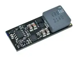
AG7010
Non Isolated POL DC/DC Converter, Module, 127 W, 3 V, 12.7 V, 10 A
⚠️ Reference pricing provided. In case of supply shortages, we will connect you with our trusted procurement partners to ensure your project's continuity.
- Manufacturer: SILVERTEL
- Product type: DC / DC Non Isolated Board Mount Converters - Adjustable Output
- SVHC: No SVHC (27-Jun-2024)
- Depth: 37.4mm
- Width: 14.4mm
- Height: 8.16mm
- Product Range: -
- Output Power Max: 127W
- Output Current Max: 10A
- Output Voltage Max: 12.7V
- Output Voltage Min: 3V
- Input Voltage DC Max: 24V
- Input Voltage DC Min: 8V
- DC / DC Converter Type: Module
- Power Supply Applications: -
- DC / DC Converter Output Type: Adjustable
| Delivery and price | |
|---|---|
| Units per pack | 50 |
| Price | 9.7 € |
| Current stock | 25+ |
| Lead time | 30 days |
Datasheet

V1.0 February 2022 Datasheet ## _Silvertel_ ## **Ag7010 High Efficiency Point of Load Buck Converter Module** ## **Features** - ➢ >97% efficient DC/DC converter - ➢ PMBus enabled - ➢ 3V-12.7V output voltage - ➢ 10A output current - ➢ Wide input voltage range 8V-24V - ➢ Very low heat output - ➢ Low output ripple & noise - ➢ Configurable UVLO, OVLO and thermal protection - ➢ Overload & short-circuit protection - ➢ Industrial temperature range - ➢ Minimal external components required - ➢ Low profile SMT package size – 37.4mm (L) x 14.4mm (H) - ➢ Silvertel “design-in” assistance ## **Description** The Ag7010 is a low noise DC/DC buck converter featuring integrated PMBus commands through I[2] C for use in a wide variety of point of load (PoL) and DC-DC converter applications including USB Powered Device (PD), Apple Lightning and Intel Thunderbolt. The high efficiency DC/DC converter can achieve greater than 97% efficiency and operates over a wide input voltage range with low noise performance and low output ripple. The DC/DC converter also has built-in output overload, output short-circuit and over-temperature protection. © Silver Telecom 2022 **Ag7010 High Power PoL DC/DC Module** Datasheet V1.0 February 2022 ## **Table of Contents** |**1**|**Product Overview ................................................................................................................................... 4**|**Product Overview ................................................................................................................................... 4**| |---|---|---| ||1.1|AQ7010 Product SeleCtOr....ccscscssccssecsscssecsssssssssesssesssecssscsescsescsesesesesesesssseeceecsescsescsesesessesessseeesssesescseseseses4| ||1.2|Package FOrmat.....ccccscssccssseccssecsssescseccsseseseeessesessesesseeseseeseseeseseescseesessesessesessesesseeecseesesuesesuesesuesesuttessssecssesesse<br>D| ||1.3|PIN D@SCTIPLION ..........cccccceesssccsesssceccssseeecesuseecessseccessseecesaseescesssecsessueeceesuseeceaseesesuseecesseesessuseesessutesssseecsecssaeesD| |**2**|**Functional Description ........................................................................................................................... 6**|| ||2.1|Typical CONNECTIONS .......cccccececsseecsseeesseeeseesseecseeseeessseeseeeesseesesesesseeesseecseeseeeseseeseseesesesesesssesssessesceeessssO| ||2.3<br>2.4|Enable/Disable..........cccccecsessscssecssecssecssececcseccsesesessseceecseccseseseseseseseceeessscsescaesesesesesssecsecatesesestssessssesssessssesO<br>POWED GOO...ceeccecesecesseccsseesseeecseeceseeseeeeeeseseseeeeescssesessescsseeeseeeceseecsesceseseeseecesesessuecesueenseesesessssssssssesseesesseesO| ||2.5.1<br>2.5.2|Ma€XiMUM OUtPUt POWETS....ccccceccsseccssecssseccseesssesessesessesessesessesesueseeusesseseuesesuesesesesusesesssesetsecsseessteeeeseL<br>Output Voltage Adjust Setting 00... eeecceccsecsseceseecsssessssecsssessseeessseseseesessesessessssesessescsesesessescssesesieeeD| |**3**|**Efficiency ................................................................................................................................................. 8**|| |**4**|**I2C Interface ............................................................................................................................................. 9**|| ||4.1<br>4.2|I2C Module ACCIeSS ...cceccsscsssecsetessecsetesecsssesecsstessecsstessecsstessecssessessssessecsseessecssiessessesessesssassesitssssesiteacecsssessOD<br>12S ProtOCOl......c.cccccescsccscsccscescsccsesscsesesscsessesacsessesacsessesaesessessesecsescsesacsecsesaesecsecacsecsesassecstsatscatsatssssecstesssecstere<br>10| ||4.2.1|Write Byte 0...<br>eeeeeeeeeeeeeeeseeeeeesseeeeeeneeeeeeseaeeecssaeeeeessaeeeesseeesesueeessseeeeeeteeeesseeeessseeersseeerseeeeseeees<br>TO| ||4.2.2|REA Byte oo...<br>eeeccesecceeeceseecsseeeeneeesseeeeseeesseeeeeesessecesaeeessecesseeesaeeeseessaeesseseseesseeestssssesesseeeeees 10| ||4.2.3<br>4.3|Block Read, BlOCK Write ..........cccccccccccccccccecececceecececeeeeeeeeeeecececeseceeeeeeceeeeeececeseeeessesesecesesecesseesssessesseseeeeees<br>TO<br>PMBUS COMMAS...........ccccccecccssceseesseeeseeeseceecseeeseccsecesecaecsaecssecsuecseccsesesecceeseeecseecseecseessesesessssssssssssssessesseeTT| ||4.3.1|Device Configuration COMMANdS............:ceceeceeseesseseeseeeeceeceeceeceeeseesaeseececeeseassaesaeeaeeeseesseesateateeeeeeseters 12| ||4.3.2|OverTemperature faultand warning Setting ...........ceeecesecsseeeeeeesseeceeecseeeeneeesseeesteeestseeeseesteesseessee TO| ||4.3.3|Monitoring COMMANAS..........cceeseseceetecseeeeseeesseeeeseeeeseeesseeessaeeceaeeesaeeeseeesaeeesseeeseeeseeeseesseseseseeeeees<br>TO| ||4.3.4|Storing Configuration 00...ceeeseeccseceeceeceseesesseseceaeeseceeceeceeceeesaeeaecaeceeecseseessaesaesaeeaeenessesseseaseteeenteets TO| ||4.3.5|Device Information COMMAMNAS............cccccccesccesesseeeeesseeesccsecseecseesseceseesecsecsecsesssssseessesssesssestsestestee TOD| |**5**|**Operating Temperature Range ............................................................................................................ 16**|| ||5.1|Thermal Considerations............cccccccecececceseeeeeeecseeeeseeceeeeceseeeeeeseseeecseeeeseeecsseecneeecsseseseeecsseecsseecsesesseesteesseeee DL| |**6**|**EMC ........................................................................................................................................................ 17**|**EMC ........................................................................................................................................................ 17**| |**7**|**Protection .............................................................................................................................................. 18**|| ||7.1|INPUt Protection ............ cccccsccccesssccesssscecesseeecesseceeesseeeccesaeeecesueecessseeecesutecesssseecessseecessseeesssseessstseesesssseesssseeees TO| ||7.2|Output Back Feed Protection ...........ccccecssecesseeesseeeseecseeeseecseeeseecseeeseeeeeeeeseeeesaeessseecseecsaeecseseeeeseeeees 1O| ||7.3|Output Short Circuit Protection...........ccccceccecssecsseeesseecseeeeseeeseeeseeeceeeesseecesseesseesesaeessseeesseecsaeecesesesesseeeees 1O| ||7.4|Thermal Protection ............cccccccccececeeeeeeeeeeeeeeeeceeeeeeceeeeeeecesaeeeceeeeeecseaeeesetaeeeeeeeeeseseeesestseeseeteeeessseeessseeeessee QD| |**8**|**Solderability ........................................................................................................................................... 19**|| ||8.1<br>8.2|Nozzle RECOMMENAALION ......... eeeeeeeeeeceeeeeeeeeeeeeeeeeeeeeeeeeaeeeceseeeeseeeaeeeeeeeeecceeaeeeceeeeeeseeeeeeseseeesestseessteeesseteee VQ<br>Solder Profile.........ccccccccceccscccsccssecseecseecseccseeseccsececcseecseecseeeseceseceeeesseceecseecsecssecesesesecssecssscssssessssssseseeseees20| |**9**|**Electrical Characteristics ..................................................................................................................... 21**|| ||9.1<br>9.2<br>9.3|Absolute Maximum RattingS..........:::cccccccsceseseeeneeseneeceneeseeeeeaeeesaeeeseeesseesseesseeesseeeseeeesseeesseeeseseessseesseeeseessee2<br>Recommended Operating Conditions 00.0...ceeececeeceseeseeeeeecseceeceeceecseesaesaeceeseeseeseeesaesaesaeseseeseassatsatsrentees21<br>DC Electrical Characteristics ........0..ccccccccccccccsecsseeeeeesecesecesecseeceeeseecsescsesesecceeceeeceeecseecseessescsessssssasssssesseessessee21| |**10**|**Package and Footprint ......................................................................................................................... 22**|| © Silver Telecom 2022 2 **Ag7010 High Power PoL DC/DC Module** Datasheet V1.0 February 2022 ## **Table of Figures** Figure 1: Block Diagram .................................................................................................................................... 4 Figure 2: Ag7010 Package Format .................................................................................................................... 5 Figure 3: Typical System Diagram .................................................................................................................... 6 Figure 4: Output Voltage Adjustment ................................................................................................................ 7 Figure 5: Ag7010 Efficiency with 12V Supply .................................................................................................... 8 Figure 6: Ag7010 Efficiency with 20V Supply .................................................................................................... 8 Figure 7: Ag7010 Efficiency with 24V Supply .................................................................................................... 9 Figure 8: Writing to a Register ......................................................................................................................... 10 Figure 9: Reading a Register ........................................................................................................................... 10 Figure 10: Block Read, Block Write ................................................................................................................. 10 Figure 11: Ag7010 operating temperature profile ............................................................................................ 16 Figure 12: Thermal Relief ................................................................................................................................ 17 Figure 13: Input Protection .............................................................................................................................. 18 Figure 14: Nozzle Centre Point ....................................................................................................................... 19 Figure 15: Package Dimensions ...................................................................................................................... 22 Figure 16: Land Pattern ................................................................................................................................... 22 **Table of Tables** Table 1: Ordering Information ............................................................................................................................ 4 Table 2: Pin Description..................................................................................................................................... 5 Table 3: Common Output Voltage Adjustments with standard Resistor Values ............................................... 7 Table 4: Command List.................................................................................................................................... 11 Table 5: Operation Byte ................................................................................................................................... 12 Table 6: ON_OFF_CONFIG Byte .................................................................................................................... 12 Table 7: General FAULT_RESPONSE Byte ................................................................................................... 12 Table 8: Output Current FAULT_RESPONSE Byte ........................................................................................ 12 Table 9: I[2] C Status Word ................................................................................................................................. 13 Table 10: STATUS_VOUT Byte ...................................................................................................................... 14 Table 11: STATUS_IOUT Byte ........................................................................................................................ 14 Table 12: STATUS_INPUT Byte ..................................................................................................................... 14 Table 13: STATUS_TEMPERATURE Byte ..................................................................................................... 14 Table 14: STATUS_CML Byte ......................................................................................................................... 14 Table 15: Solder Profile ................................................................................................................................... 20 Table 16: Solder Parameters ........................................................................................................................... 20 © Silver Telecom 2022 3 **Ag7010 High Power PoL DC/DC Module** Datasheet V1.0 February 2022 ## **1 Product Overview** ## **Ag7010 Product Selector** |**Part**<br>**Number1**|**Nominal Output**<br>**Voltage**|**Output Current**|**Marking2**| |---|---|---|---| |Ag7010|3V|10A Continuous|ab05c| - Note 1: Complies with the European Directive 2011/65/EU for the Restriction of use of certain Hazardous Substances (RoHS) including Directive 2015/863 published in 2015, amending Annex II of Directive 2011/65/EU. Moisture Sensitivity Level 1 and HBM 1. - Note 2: The first letter, a, indicates the week as A-Z with uppercase being weeks 1-26, lower case weeks 27-52. The second letter, b, indicates the year in uppercase A-Z starting from 2020. The two digits are the nominal output voltage, - The final letter, c, is a Silvertel reference. **Table 1: Ordering Information** **==> picture [375 x 191] intentionally omitted <==** **----- Start of picture text -----**<br> 7010 ADJ<br>Vin+ Vout+<br>PG<br>DC:DC<br>CONTROL<br>+ Monitoring Converter DC<br>& Control<br>Output<br>Vin- Vout-<br>I [2] C<br>- SCL<br>- SDA<br>- ADD0<br>[a] - ADD1<br>**----- End of picture text -----**<br> **Figure 1: Block Diagram** © Silver Telecom 2022 4 **Ag7010** Datasheet **High Power PoL DC/DC Module** V1.0 February 2022 ## **Package Format** ||7||6||5|4|3|| |---|---|---|---|---|---|---|---|---| |||||£y|Ag7010<br> Silvertel|||1<br>2| |8||9|10||12<br>11|||4| ||||||Top View|||| **Figure 2: Ag7010 Package Format** ## **Pin Description** |**Pin #**|**Name**|**Description**| |---|---|---| |1|PG|**Power Good.**High signal indicates supply power.| |2|CONTROL|**DC/DC Converter Enable Control.**Pull this pin low to disable the<br>DC/DC converter, can be inverted or disabled as per PMBus specification| |3|IC|**Internal Connection.**Do not connect to this pin.| |4|ADD0|**I2C Address bit0.**Internally pulled HIGH| |5|ADD1|**I2C Address bit1.**Internally pulled HIGH| |6|Vin+|**High Supply.**This pin connects to the positive (+) supply| |7|Vin-|**Low Supply.**This pin connects to the reference of the positive supply| |8|SCL|**Serial Clock Input.**This high impedance input pin connects to the I2C<br>bus clock.| |9|SDA|**Serial Data Analogue Input.**This high impedance input pin is used in<br>conjunction with the SCL pin to for the I2C bus.| |10|ADJ|**Output Adjust.**The output voltage can be adjusted from its nominal<br>value, by connecting an external resistor from this pin the Vout- pin.| |11|Vout-|**Negative DC Output.**This pin provides the negative regulated output<br>from the Ag7010 and is internally connected to pin 7.| |12|Vout+|**Positive DC Output.**This pin provides the positive regulated output from<br>the Ag7010.| **Table 2: Pin Description** © Silver Telecom 2022 5 **Ag7010 High Power PoL DC/DC Module** Datasheet V1.0 February 2022 ## **2 Functional Description** ## **Typical Connections** The Ag7010 requires only a few external components for operation. The 470µF capacitor (C1) connected across the input is required for correct operation of the DC/DC converter. This capacitor must be positioned as close to the input pins as possible for optimal stability. This can be a low-cost electrolytic capacitor for operation in temperatures down to 0C (a minimum of 470µF 16V is recommended for 12V supply) as shown in Figure 3. If ambient temperatures below 0°C are expected, a capacitor that retains a moderately low ESR and the minimum capacitance is essential for operation. Polymer Aluminium Solid Electrolytic Capacitors are ideal for this application. The output voltage can be adjusted by simply connecting a resistor, R1, between the ADJ pin and the Vout– pin, see section 2.5.2 Output Voltage Adjust Setting for more details. **==> picture [339 x 195] intentionally omitted <==** **----- Start of picture text -----**<br> Input Vin+ Vout+ Output<br>Supply Load<br>+<br>C1 C2 £9 Silvertel<br>470µF 22µF Ag7010<br>Vin- Vout-<br>- SDA —»<br>ADJ<br>R1 SCL » > To Controller *<br>4.12K PG »<br>L- CONTROL » ><br>ADD0 ADD1<br>R2 R3<br>0 0<br>*pull up resistors recommended<br>**----- End of picture text -----**<br> **Figure 3: Typical System Diagram** ## **Input** The Ag7010 has two input pins VIN+ and VIN-, these pins should be connected to an 8V24V supply (see Figure 3: Typical System Diagram). For stability it is recommended that an 470µF electrolytic and a 22µF ceramic capacitor be fitted across these pins. ## **Enable/Disable** The Ag7010 has an Enable/Disable pin, CONTROL, the default operation is pulling this pin LOW will disable the output of the module, internally pulled HIGH. This can be configured to invert or disable the pin operation as described in the PMBus specification, see section 4.3.1.2 for more details. ## **Power Good** The Ag7010 features a Power Good Output, PG, this will pull HIGH when the output has reached a regulated output voltage. This can be used for power sequencing. © Silver Telecom 2022 6 **Ag7010 High Power PoL DC/DC Module** Datasheet V1.0 February 2022 ## **Output** ## **2.5.1 Maximum output power** Whist the Ag7010 can deliver a continuous output current of 10A, with up to 120W of continuous power, the peak output power may be reduced as a result of the operating conditions the module is operating in. ## **2.5.2 Output Voltage Adjust Setting** The Ag7010 has a nominal output of 3V, but with use of the output voltage adjustment pin, ADJ, this can be increased to a maximum of 12.7V at the output of the Ag7010. **==> picture [125 x 156] intentionally omitted <==** **----- Start of picture text -----**<br> +VDC<br>Silvertel ADJ<br>Ag7010<br>Radj<br>-VDC<br>Increasing the output<br>voltage from nominal<br>**----- End of picture text -----**<br> **Figure 4: Output Voltage Adjustment** |𝑹𝒂𝒅𝒋=<br>𝟑𝟕. 𝟐𝒌<br>𝑽𝑶𝑼𝑻−𝟑. 𝟎𝟖|𝑹𝒂𝒅𝒋=<br>𝟑𝟕. 𝟐𝒌<br>𝑽𝑶𝑼𝑻−𝟑. 𝟎𝟖|𝑹𝒂𝒅𝒋=<br>𝟑𝟕. 𝟐𝒌<br>𝑽𝑶𝑼𝑻−𝟑. 𝟎𝟖|𝑹𝒂𝒅𝒋=<br>𝟑𝟕. 𝟐𝒌<br>𝑽𝑶𝑼𝑻−𝟑. 𝟎𝟖|𝑹𝒂𝒅𝒋=<br>𝟑𝟕. 𝟐𝒌<br>𝑽𝑶𝑼𝑻−𝟑. 𝟎𝟖| |---|---|---|---|---| |Radj||||| |Desired Output voltage|3V|3.3V|5V|12V| |Recommended standard<br>resistor Value of RA|OC|169K|19.1K|4.12K| **Table 3: Common Output Voltage Adjustments with standard Resistor Values** Note 1: It is important that the output is not taken above 12.7V. Setting the output voltage above this level may result in the module being permanently damaged. © Silver Telecom 2022 7 **Ag7010 High Power PoL DC/DC Module** Datasheet V1.0 February 2022 ## **3 Efficiency** The Ag7010 has been designed as a high efficiency DC/DC solution, ## **Figure 5: Ag7010 Efficiency with 12V Supply** ## **Figure 6: Ag7010 Efficiency with 20V Supply** © Silver Telecom 2022 8 **Ag7010 High Power PoL DC/DC Module** Datasheet V1.0 February 2022 **Figure 7: Ag7010 Efficiency with 24V Supply** ## **4 I[2] C Interface** The Ag7010’s I[2] C interface supports PMBus commands and is designed to the PMBus rev 1.3 specification. This allows for the configuration, control and monitoring of the DC/DC converter by a system controller. The Ag7010 is a slave device using two pins to connect to the I[2] C interface SCL (serial clock) and SDA (serial data). The interface connection should be referenced to the negative input supply Vin- and is compatible with a 3V and 5V bus. The interface signals are unbuffered prior to the microcontroller on the Ag7010. If a long cable is to be used carrying the I[2] C signals, buffering should be added to protect the Ag7010 from damage. It is advisable to include 10kΩ pullup resistors on the SCL and SDA lines. ## **I[2] C Module Address** Up to four Ag7010 Modules can operate on the same I[2] C communication bus by configuring the module address, this can be performed by pulling pins ADD0 and ADD1 low to change the I[2] C address of the module, a power cycle may be required if the I[2] C address is modified while the module is powered. The modules Address byte will be 10101A1A0W, where A is the logic level of the ADD0 and ADD1 pins, and W is the read/write command. © Silver Telecom 2022 9 **Ag7010** Datasheet V1.0 February 2022 **High Power PoL DC/DC Module** ## **I[2] C Protocol** ## **4.2.1 Write Byte** Writing to a register in the slave device is performed with the protocol below. **==> picture [407 x 86] intentionally omitted <==** **----- Start of picture text -----**<br> SCL<br>SDA A6 A5 A4 A3 A2 A1 A0 R/W ACK F7 F6 F5 F4 F3 F2 F1 F0 ACK D7 D6 D5 D4 D3 D2 D1 D0 ACK<br>Module Address Byte Command Code Byte Data Byte<br>Master ee P| DOO<br>Ag7010 = 7 _—<br>**----- End of picture text -----**<br> **Figure 8: Writing to a Register** ## **4.2.2 Read Byte** To read a register from the slave device the below protocol is used. If more than one byte is to be requested, then the master should respond to the data byte with an Acknowledge until it has received the expected number of bytes. **==> picture [431 x 75] intentionally omitted <==** **----- Start of picture text -----**<br> SCL<br>SDA —" A6 f_\ A5 A4 [ A3 A2 iV A1 A0 \ R/W _ ACK [_\ F7 F6 F5 VV F4 F3 VV F2 F1 A [\ F0 ACK N\ A6 I A5 \ A4 [VV A3 A2 A1 \ A0 7 R/W ACK \ D7 VV D6 D5 D4 Vv D3 VO D2 VV D1 D0 j— ACK \<br>Module Address Byte Command Code Byte Sto p &Start M odule Address Byte + 1 Data Byte<br>Master De | Dh =<br>Ag7010 zz =z ee<br>**----- End of picture text -----**<br> **Figure 9: Reading a Register** ## **4.2.3 Block Read, Block Write** Some of the supported PMBus commands implement a Block Read or Block Write & Block Read protocol. In the case of a block read or write command, the first transmitted data byte will be a count of the data bytes that are to follow. **==> picture [429 x 159] intentionally omitted <==** **----- Start of picture text -----**<br> SCL<br>SDA "7 A6 f_\ A5 A4 Veo A3 A2 A1 ON A0 R/W ACK F7 VV F6 F5 F4 VV F3 F2 VY VO F1 F0 ACK rE D7 D6 D5 D4 ON D3 OM D2 D1 D0 ACK VV D7 D6 D5 D4 D3 D2 D1 D0 ACK<br>\ DV DRO DOOYOO DOOYOO IOAN FY OIA OV VA IO A O_ON<br>Module Address Byte Command Code Byte Byte Count Data Byte 0<br>Master ee | es es<br>Ag7010 | | Lt Lt<br>SCL<br>SDA ACK N A6 rT A5 A4 VO A3 A2 VV A1 A0 R/W ACK 7 \ D7 [Veen D6 Veen D5 ven D4 D3 en D2 en D1 en D0 | ACK rVV D7 D6 D5 VY D4 VY D3 WY D2 D1 D0 ACK D7 VV D6 D5 D4 VV D3 D2 VY D1 VY D0 ACK<br>Sto p &Start M odule Address Byte + 1 Byte Count Data Byte 0 Data Byte 1<br>poe af ke a] be o te 4<br>Master |<br>Ag7010 fe |<br>**----- End of picture text -----**<br> **Figure 10: Block Read, Block Write** © Silver Telecom 2022 10 **Ag7010 High Power PoL DC/DC Module** Datasheet V1.0 February 2022 ## **PMBUS commands** |Information|Information|Information|Information|Information|Information|Information|Monitoring|Monitoring|Monitoring|Monitoring|Monitoring|Monitoring|Monitoring|Monitoring|Monitoring|Monitoring|Monitoring|Memory|Memory|Memory|Memory|Memory|Temperature<br>Configuration|Temperature<br>Configuration|Temperature<br>Configuration|Iout Configuration|Vout Configuration|Vout Configuration|Vout Configuration|Input Configuration|Input Configuration|Input Configuration|Input Configuration|Input Configuration|Input Configuration|Input Configuration|Input Configuration|ON OFF<br>Configuration|ON OFF<br>Configuration|| |---|---|---|---|---|---|---|---|---|---|---|---|---|---|---|---|---|---|---|---|---|---|---|---|---|---|---|---|---|---|---|---|---|---|---|---|---|---|---|---|---| |MFR_REVISION|MFR_MODEL|MFR_ID|PMBUS_REVISION|VOUT_MODE|QUERY|CAPABILITY|READ_TEMPERATURE_1|READ_VOUT|READ_VIN|STATUS_CML|STATUS_TEMPERATURE|STATUS_INPUT|STATUS_IOUT|STATUS_VOUT|STATUS_WORD|STATUS_BYTE|CLEAR_FAULTS|RESTORE_DEFAULT_CODE|STORE_DEFAULT_CODE|RESTORE_DEFAULT_ALL|STORE_DEFAULT_ALL|RESET_REGISTERS|OT_WARN_LIMIT|OT_FAULT_RESPONSE|OT_FAULT_LIMIT|IOUT_OC_FAULT_RESPONSE|VOUT_OV_WARN_LIMIT|VOUT_OV_FAULT_RESPONSE|VOUT_OV_FAULT_LIMIT|VIN_UV_FAULT_RESPONSE|VIN_UV_FAULT_LIMIT|VIN_UV_WARN_LIMIT|VIN_OV_WARN_LIMIT|VIN_OV_FAULT_RESPONSE|VIN_OV_FAULT_LIMIT|VIN_OFF|VIN_ON|ON_OFF_CONFIG|OPERATION|Command Name| |9Bh|9Ah|99h|98h|20h|1Ah|19h|8Dh|8Bh|88h|7Eh|7Dh|7Ch|7Bh|7Ah|79h|78h|03h|14h|13h|12h|11h|C4h|51h|50h|4Fh|47h|42h|41h|40h|5Ah|59h|58h|57h|56h|55h|36h|35h|02h|01h|Command<br>Code| |✓*|✓*|✓*|✓|✓|-|✓|✓|✓|✓|✓|✓|✓|✓|✓|✓|✓|-|-|-|-|-|-|✓|✓|✓|✓|✓|✓|✓|✓|✓|✓|✓|✓|✓|✓|✓|✓|✓|Read| |-|-|-|-|-|✓**|-|-|-|-|✓|✓|✓|✓|✓|✓|✓|✓|✓|✓|✓|✓|✓|✓|✓|✓|✓|✓|✓|✓|✓|✓|✓|✓|✓|✓|✓|✓|✓|✓|Write| |2|6|9|1|1|1|1|2|2|2|1|1|1|1|1|2|1|0|1|1|0|0|0|2|1|2|1|2|1|2|1|2|2|2|1|2|2|2|1|1|# Data<br>Bytes| |-|-|-|-|-|-|-|-|-|-|-|-|-|-|-|-|-|-|-|-|-|-|-|✓|✓|✓|✓|✓|✓|✓|✓|✓|✓|✓|✓|✓|✓|✓|✓|✓|Mem<br>store| |-|"Ag7010"|"Silvertel"|0x33|0x40|-|0x20|-|-|-|-|-|-|-|-|-|-|-|-|-|-|-|-|162 (115C)|0xF8|125 (125 C)|0xFB|2177 (12.8V)|0xF8|2212 (13V)|0xF8|615 (6.25V)|590 (6.4V)|2420 (26.1V)|0xF8|2480 (26.8V)|568 (6.1V)|625 (6.75V)|0x1F|0x80|Default<br>Value| |-|-|-|-|-|-|-|-|-|-|-|-|-|-|-|-|-|-|-|-|-|-|-|2048 - 182 (25-110c)|-|2048 - 125 (25-110c)|-|595 - 2213(3.5-13V)|-|596 - 2212 (3.5-13V)|-|566 - 2480 (6-26.5V)|567 -2480 (6-26.5V)|625 - 2481 (7-26.5V)|-|625 - 2480 (7-26.5V)|568 - 2480 (6 -26.5V)|568 - 2480 (6 -26.5V)|-|-|Range| |ASCII Code|ASCII Code|ASCII Code|-|-|-|-|See Datasheet for<br>Formula|<<br>2)<br>M<br>Be<br>a a <br>Bl|8<br>“<br>"<br>ire}<br> S| a<br>|e|-|-|-|-|-|-|-|-|-|-|-|-|-|See Datasheet for<br>formula||See Datasheet for<br>formula|-|5<br>nl<br>a<br>=<br>S<br>Bb<br>x<br>=|<br>8|-|®<br>H<br>ua<br>|<br>°<br>BR<br>x<br>[sl<br>5|-|a<br>Wy<br>wo]<br>NY]<br>trl<br>we]<br>[sists]|a<br>oud<br>oO]<br>NY]<br>i]<br>KY]<br>[sists]|a<br>oud<br>oO<br>[sists]|-|a<br>Wyo}<br>wo]<br>N]<br>tal<br>x)<br>|sl)sis|a<br>Wyo}<br>oO;<br>S|<br>i]<br>RM] <br>|sl)sis|a<br>Wyo}<br>oO<br>ia<br> x<br>|sl)sis|-|-|Conversion| |0xBC|0xBC|0xBC|0xBC|0xBC|0xBC|0xBC|0xB8|0xB8|0xB8|0xFC|0xFC|0xFC|0xFC|0xFC|0xFC|0xFC|0xDC|0xD0|0xD0|0xDC|0xDC|0xDC|0xF8|0xFC|0xF8|0xFC|0xF8|0xFC|0xF8|0xFC|0xF8|0xF8|0xF8|0xFC|0xF8|0xF8|0xF8|0xFC|0xFC|QUERRY<br>Command<br>Response| |States the Modules Hardware (MSB) and Firmware (LSB) Revision|States the Module Model|States the Module Manufacturer|States the Module is compliant to PMBus part I and II revision 1.3|The states format the output voltage is relayed. The module Directly provides a Byte value<br>that is converted usingthe formula in the conversion column|Query Commands to the determine the operations that can be performed it|States the supported PMBus capability options. See datasheet for more details|states the module Temperature Measurement|states the Output Voltage Measurement|states the Input Voltage Measurement|Read or Clear the Communication Status Byte|Read or Clear the Temperature Status Byte|Read or Clear the Input Status Byte|Read or Clear the Output Current Status Byte|Read or Clear the Output Voltage Status Byte|Returns the Status Word|Returns the Status Byte, this is the same as the lower Byte of the Status Word|Clears all status flags|Restore the command specified in the data byte to the default setting|Store the setting related to command specified in the data byte as the default setting|restores the Default settings|Store all current settings that support memory Store as the default settings|restores all settings to the value in the Default value column|Configure the Temperature that will trigger the "Over Temperature Warning" flag|Configure how the module recovers from an over temperature fault|Configure the Temperature that will trigger the "Over Temperature Fault" flag|Configure how the module recovers from an over current fault|Configure the voltage that will trigger the "Output Over Voltage Warning" flag|Configure how the module recovers from an over voltage fault|Configure the voltage that will trigger the "Output Over Voltage Fault" flag|Configure how the module recovers from an under voltage fault|Configure the voltage that will trigger the "Input Under Voltage Fault" flag|Configure the voltage that will trigger the "Input Under Voltage Warning" flag|Configure the voltage that will trigger the "Input Over Voltage Warning" flag|Configure how the module recovers from an over voltage fault|Configure the voltage that will trigger the "Input Over Voltage Fault" flag|Configure the voltage the module will disable the output|Configure the voltage required before the module will enable the output|Configure the ON/OF control for the module|Enable or disable the output of the module|Description| **Table 4: Command List** © Silver Telecom 2022 11 **Ag7010 High Power PoL DC/DC Module** Datasheet V1.0 February 2022 ## **4.3.1 Device Configuration Commands** ## **4.3.1.1 OPERATION Command** The module’s output can be enabled or disabled using the I[2] C bus using bit 7 of the ON/OFF command. This is dependent on the configuration of the ON_OFF_CONFIG. |**Bit**|**Function**|**Setting**| |---|---|---| |7|ON/OFF Control|0 - DC/DC converter OFF<br>1 - DC/DC converter ON| |6:0|Not Used|-| ## **Table 5: Operation Byte** ## **4.3.1.2 ON_OFF_CONFIG Command** The ON_OFF_CONFIG command configures whether the Ag7010 output is controlled by the OPERATION command, CONTROL pin or both, this command also allows for reversing the polarity of the CONTROL pin. |**Bit**|**Function**|**Setting**| |---|---|---| |7:5|Not Used|-| |4|Control Override|0 - Converter is always ON when powered<br>1 - ON/OFF behaviour controlled by bits 2&3| |3|PMBus Control|0<br>Disables PMBus ON/OFF control<br>1 - Enables PMBus ON/OFF control| |2|EN-DIS pin Control|0<br>Disables CONTROL pin ON/OFF control<br>1 - Enables CONTROL pin ON/OFF control| |1|EN-DIS Polarity|0 - Pull CONTROL pin Low to turn ON converter<br>1 - Pull CONTROL pin Low to turn OFF converter| |0|Off Response|0 - Not Used<br>1 - Immediate Off| ## **Table 6: ON_OFF_CONFIG Byte** ## **4.3.1.3 Fault Response** The fault response commands dictate how the module will behave in the presence of the corresponding fault. |**Bit**|**Function**|**Setting**| |---|---|---| |7:6|Fault Response|11 - The Modules output is disabled and will resume normal operation once the<br>fault is removed<br>10 - Device is disabled and will attempt to restart according the retry setting<br>01 - 00 - Not Used| |5:3|Retry Setting|111 - The Module indefinitely attempts to restart<br>110 - 001 - The module attempts to restart 1-6 times before remaining off<br>000 - The Module does not attempt to restart| |2:0|DelayTime|111 - 000* - The amount of seconds delaybetween each retryattempt| - 000 only valid when configured to not use the retry setting **Table 7: General FAULT_RESPONSE Byte** **==> picture [369 x 83] intentionally omitted <==** **----- Start of picture text -----**<br> Bit Function Setting<br>11 - Device is disabled and will attempt to restart according the retry setting<br>7:6 Fault Response<br>10 - 00 - Not Used<br>111 - The Module indefinitely attempts to restart<br>5:3 Retry Setting 110 - 001 - The module attempts to restart 1-6 times before remaining off<br>000 - The Module does not attempt to restart<br>2:0 Delay Time 111 - 001 - The amount of seconds delay between each retry attempt<br>**----- End of picture text -----**<br> **Table 8: Output Current FAULT_RESPONSE Byte** © Silver Telecom 2022 12 **Ag7010 High Power PoL DC/DC Module** Datasheet V1.0 February 2022 ## **4.3.2 Over Temperature fault and warning setting** The Ag7010 uses an NTC to detect its operating temperature, this allows the temperature at which the module will trigger either the over temperature warning or the over temperature fault flags can be set to the user requirements. By default, the module will flag the over temperature warning flag when the module detects it has exceeded approximately 115˚C and will flag the over temperature fault and turn off the output when the module reaches 125˚C. The value to set these fields to can be calculated with the formula below, where 𝑎 is the register value and 𝑇𝑐 is the desired temperature in Celsius. **==> picture [169 x 46] intentionally omitted <==** ## **Equation 1: Setting Temperature Field** ## **4.3.3 Monitoring commands** ## **4.3.3.1 Read Temperature Command** Use Equation 2 to convert the register value, where 𝑎 is the register value and 𝑇𝑐 is the temperature is Celsius. **==> picture [269 x 36] intentionally omitted <==** ## **Equation 2: Reading Temperature Field** ## **4.3.3.1 Status Byte Command** The Status Byte command returns the low byte only of the Status Word in Table 9. The STATUS_BYTE command reports the most important faults and warning, bit 0 of the STATUS_BYTE is used to highlight that there is a flag in the Higher byte that may require attention. ## **4.3.3.2 Status Word Command** |**Byte**|**Bit**|**Function**|**Description**| |---|---|---|---| |Low|7|Busy|The Module is not currently able to accept and process commands from the bus| ||6|Off|DC/DC converter is OFF| ||5|Output Over Voltage fault|An Over Voltage Fault has occurred| ||4|Over Current Fault|An Over Current Fault has occurred| ||3|Input undervoltage fault|An Input Under Voltage Fault has occurred| ||2|Temperature Status flagged|At least one Bit in STATUS_TEMPERATURE has flagged| ||1|Communication fault|At least one Bit in STATUS_CML has flagged| ||0|Other fault detected|A flag in the High Byte that is not reflected in a Low Byte Flag is present| ||||| |High|7|Output Voltage Status|At least one Bit in STATUS_VOUT has flagged| ||6|Output Current Status|At least one Bit in STATUS_IOUT has flagged| ||5|Input Status Flagged|At least one Bit in STATUS_INPUT has flagged| ||4|Not Used|-| ||3|Power Good Status|Indicates the Power is good when low| ||2|Not Used|-| ||1|Not Used|-| ||0|Other fault or warning|Miscellaneous error has occurred| **Table 9: I[2] C Status Word** © Silver Telecom 2022 13 **Ag7010 High Power PoL DC/DC Module** Datasheet V1.0 February 2022 ## **4.3.3.3 Voltage Output Status Command** |**Bit**|**Function**|**Description**| |---|---|---| |7|Output Over Voltage Fault|The Output Voltage has exceeded the VOUT_OV_FAULT_LIMIT setting| |6|Output Over Voltage Warning|The Output Voltage has exceeded the VOUT_OV_WARN_LIMIT setting| |5:0|Not Used|-| |**Table 10: STATUS_VOUT Byte**<br>**Current Output Status Command**||| |**Bit**|**Function**|**Description**| |7|Over Current/On Time fault|The output was removed due to an Overcurrent event| |6:0|Not Used|-| |**Table 11: STATUS_IOUT Byte**<br>**Input Status Command.**||| |**Bit**|**Function**|**Description**| |7|Input Over Voltage Fault|The Input Voltage has exceeded the VIN_OV_FAULT_LIMIT setting| |6|Input Over Voltage Warning|The Input Voltage has exceeded the VIN_OV_WARN_LIMIT setting| |5|Input Under Voltage Warning|The Input Voltage has dropped below the VIN_UV_WARN_LIMIT setting| |4|Input Under Voltage Fault|The Input Voltage has dropped below the VIN_UV_FAULT_LIMIT setting| |3|DCDC converter Disabled due to under voltage|Converter shut down due to being below Voff or not having risen above Von| |2:0|Not Used|-| ## **4.3.3.4 Current Output Status Command** ## **4.3.3.5 Input Status Command.** ## **Table 12: STATUS_INPUT Byte** ## **4.3.3.6 Temperature Status Command** |**Bit**|**Function**|**Description**| |---|---|---| |7|Over Temperature Fault|The Temperature Voltage has exceeded the OT_FAULT_LIMIT setting| |6|Over Temperature Warning|The Temperature has exceeded the OT_WARN_LIMIT setting| |5:0|Not Used|-| ## **Table 13: STATUS_TEMPERATURE Byte** ## **4.3.3.7 Communication status Command** |**Bit**|**Function**|**Description**| |---|---|---| |7|Invalid Command Received|A command that the Module does not support has been received| |6|Invalid Data Received|A unsupported data value has been received| |5:2|Not Used|-| |1|Other Communication fault|A communication fault not covered above has occurred| |0|Memoryor Logic fault|A logic or memoryfault has occurred| **Table 14: STATUS_CML Byte** ## **4.3.3.1 Clearing status flags** When one of the status bits has flagged it will remain flagged until it is either cleared, or power is removed from the module. The clearing of a status flag can be performed in one of two ways, either by sending a write request to the CLEAR_FAULTS command, or by writing a logic HIGH to the bit of the corresponding flag in the relevant status byte. The only bits that can be cleared by writing to the STATUS_BYTE or STATUS_WORD registers are bit 7 of the low byte (Busy) and bit 0 of the high byte (Other fault or warning). All other bits are either reporting that a flag in the corresponding status register has been set or will clear when the condition is no longer true, i.e. ‘Off’ and ‘Power Good Status’ © Silver Telecom 2022 14 **Ag7010 High Power PoL DC/DC Module** Datasheet V1.0 February 2022 ## **4.3.4 Storing Configuration** All Configuration changes are volatile until saved using either the STORE_DEFAULT_ALL or STORE_DEFAULT_CODE commands. These will then be retained on powerup or reapplied with the RESTORE_DEFAULT_ALL or RESTORE_DEFAULT_CODE commands The RESET_REGISTERS command will clear all stored values and revert back to the manufacturer defaults detailed in Table 4: Command List. ## **4.3.5 Device Information Commands** ## **4.3.5.1 Capability Command** The capability field is a read only command that states the supported functionality of the module. The result of reading this field states that the module supports a maximum bus speed of 400kHz, does not use the IEEE half precision floating point format, does not utilise AVSBus support, SM Bus Alert response protocol or packet error checking. ## **4.3.5.2 Query Command** The Query command is used to probe the other commands to determine whether they are supported and their supported functionality for example, whether they support read/write commands and the data format that is used. Please refer to the PMBus specification for more details regarding this command. The Query command utilises the block Write, and the Block read protocol, shown in Figure 10. In the case below the first byte count, transmitted by the master, will be 1 as the written data contains the one byte of command code being queried. The second byte count, transmitted by the Ag7010, in this transaction will also be 1. © Silver Telecom 2022 15 **Ag7010 High Power PoL DC/DC Module** Datasheet V1.0 February 2022 ## **5 Operating Temperature Range** The Ag7010 is a DC/DC converter. Whilst this has been designed to be one of the highest efficiency modules on the market, it is still a power device and thus will generate heat, so it is important that this is taken into consideration at the design stage. The amount of heat generated by the module will depend on the load it is required to drive and the input voltage. The Ag7010 can operate up to a maximum of 85˚C ambient, and a minimum of -40˚C ambient. When intended for use in ambient temperatures below 0C it is recommended that an input capacitor that will retain capacitance and ESR ratings at the lowest temperature in the intended operating range is used. A reputable brand capacitor rated to - 55C should suffice for most applications, please contact Silvertel if suggestions are required. The graph below shows the continuous load capabilities of the module across environmental temperatures, for a range of common input output configurations. These results have been recorded in a Temperature Applied Sciences ECO MT135 Environmental chamber (with circulating air) with forced airflow across the module at a rate of 1.5m/s. Under these conditions the Ag7010 is capable of sourcing its full output power for any given input and output voltage across an operating temperature range of -40C to +65C. Operation in a sealed enclosure or with limited airflow will result in further de-rating of the operating temperature profile. **Figure 11: Ag7010 operating temperature profile** © Silver Telecom 2022 16 **Ag7010 High Power PoL DC/DC Module** Datasheet V1.0 February 2022 ## **Thermal Considerations** Each application is different; therefore, it is impossible to give fixed and absolute thermal recommendations. Due to the small size of this module, it is important that heat is drawn out and away. It is also important that any enclosure has sufficient ventilation for the Ag7010. One simple method for drawing some of the heat away from the Ag7010 is by means of power planes connected to the power pads of the module Vin+, Vin-, Vout+, and Vout-. These power planes must be on the outer layers of the PCB and the best results are achieved by having power planes on both sides of the main board with regular via connections to thermally bond the planes. An example of the topside layout is shown in Figure 12. It should be noted that there are exposed pads on the underside of the module that should be left unconnected, no exposed copper should be present in this region. See Section 10: Package and Footprint. **==> picture [230 x 247] intentionally omitted <==** **----- Start of picture text -----**<br> +<br>Ag7010<br>?<br>Exposed Copper Thermal relief<br>Keep Out power planes<br>**----- End of picture text -----**<br> **Figure 12: Thermal Relief** ## **6 EMC** The Ag7010 has been designed to pass EN55032 Class B, however the Ag7010 will only be a single component within the system, depending on the application, filtering of the emissions passing through the Ag7010 may be required. © Silver Telecom 2022 17 **Ag7010 High Power PoL DC/DC Module** Datasheet V1.0 February 2022 ## **7 Protection** ## **Input Protection** To reduce the risk of damage, the Ag7010 will shut down the DC/DC converter if an input voltage exceeding either the VIN_OV_FAULT_LIMIT or the maximum supply rating is detected. The Ag7010 may still be damaged if input voltages exceed 28V. Over voltage protection such as a TVS diode can be fitted across the VIN+ and VIN- input pins, providing protection from electrostatic discharge (ESD) or other high voltage transients. One example of this is the SMAJ24A. **==> picture [289 x 195] intentionally omitted <==** **----- Start of picture text -----**<br> 24V Vin+ Vout+<br>SMAJ24A * +<br>Ag7010<br>Vin- Vout-<br>ADJ SDA<br>ADD0 SCL<br>ADD1 PG<br>CONTROL<br>ae<br>* Note: Bidirectional Tranzorb diodes are also suitable in this configuration (SMAJ24CA)<br> If a lower voltage supply is to be used a lower clamping voltage variant may provide better protection<br>**----- End of picture text -----**<br> ## **Figure 13: Input Protection** ## **Output Back Feed Protection** If an external or auxiliary supply is to be used, it is essential that a blocking diode is present to prevent voltage injection on to the output circuitry of the module. This may cause damage to the module. The back feed protection is required even if the external voltage is present only while the module remains unpowered. ## **Output Short Circuit Protection** The Ag7010 has over-current protection to prevent the module from becoming damaged in the event of a short circuit event. If an over current event occurs the Ag7010 will disable the output, the Ag7010 will then indefinitely attempt restart according to the IOUT_OC_FAULT_RESPONSE setting. By default, the module will continuously test current draw approximately every 3 seconds until the cause of the over current is removed, after which, the power will be restored to the output. © Silver Telecom 2022 18 **Ag7010 High Power PoL DC/DC Module** Datasheet V1.0 February 2022 ## **Thermal Protection** The Ag7010 contains built-in thermal protection to prevent the module becoming damaged in the event that the module is operated beyond its temperature specification. When the Ag7010 has detected it is over temperature, the output will be disabled until the module has cooled sufficiently. For applications where there is limited airflow, it is recommended that the over temperature fault limit is reduced to prevent damage to the module. ## **8 Solderability** While the Ag7010 can be mounted by hand or hot air reflow, it has been designed with an open frame design to keep weight to a minimum allowing it to be mounted via a fully automated assembly process. The Ag7010 is lead-free (Pb-free) and RoHS compliant and fully compatible in a Pb-free soldering process. There are no specific requirements regarding stencil thickness or solder paste classification type. Non-solder mask defined (NSMD) pads are preferred over solder mask defined (SMD) pads, for the improved solderability, the land pattern dimensions are given in Figure 16: Land Pattern. The Ag7010 requires no components of greater than Moisture Sensitivity level 1, as a result no special processes are required in the reflowing process of the Ag7010. Note : Do not pass the Ag7010 through the reflow process mounted to the underside of the assembly due to the risk of components falling off the module. ## **Nozzle Recommendation** The minimum recommended nozzle diameter for reliable handling is 4mm, with a maximum diameter of 10mm. The nozzle should be applied to the inductor with the centre point located within the region specified in Figure 14. For reliable operation the nozzle should be centred in this region as close to the centre of the module as the nozzle diameter will allow. 11 **==> picture [438 x 113] intentionally omitted <==** **----- Start of picture text -----**<br> A<br>Millimetres Inches<br>Dimension<br>Typ Max Typ Max<br>A 6.40 - 0.252 -<br>Ag7010 D B 6.94 - 0.273 -<br>B C - 11.00 - 0.433<br>D - 4.50 - 0.177<br>j( -3 C ==<br>**----- End of picture text -----**<br> **Figure 14: Nozzle Centre Point** © Silver Telecom 2022 19 **Ag7010 High Power PoL DC/DC Module** Datasheet V1.0 February 2022 ## **Solder Profile** Below is a typical profile that the Ag7010 should be mounted, based on the J-STD-020 standard for PB-Free applications. Exceeding these specifications may cause damage to the module. All production environments are different therefore please review these guidelines with the process engineer prior to use. Zone 1 Zone 2 Zone 3 Zone 4 Zone 5 Units Zone Duration 42 42 42 42 42 Seconds Top Heater 150 180 210 240 270 ˚C Bottom Heater 150 180 210 240 270 ˚C Typical Slope 2.1 1.2 1.1 0.9 0.8 ˚C/Second ~~==SS=S55~~ Airflow rate 40 M[3] /Minute **Table 15: Solder Profile** Min Max Units Soak Time (s) 150-180˚C 30 90 Seconds Time above (s) ≥220˚C 30 90 Seconds Peak Temperature (˚C) 230 255 ˚C ~~nee~~ ∆Temperature (˚C/s) -3 3 ˚C/Second **Table 16: Solder Parameters** © Silver Telecom 2022 20 **Ag7010** Datasheet **High Power PoL DC/DC Module** V1.0 February 2022 ## **9 Electrical Characteristics** 9.1 **Absolute Maximum Ratings** |<br>9.1|**Absolute Maximum Ratings**||||| |---|---|---|---|---|---| ||**Parameter**|**Symbol**|**Min**|**Max**|**Units**| |1|DC Supply Voltage|VCC|-0.3|26|V| |2|Storage Temperature|TS|-40|+100|°C| |3|Moisture Sensitivity Level|MSL|-|1|-| Note : Exceeding the above ratings may cause permanent damage to the product. Functional operation under these conditions is not implied. Maximum ratings assume free airflow. ## **Recommended Operating Conditions** |~~ee~~<br>~~ee~~|**DC Characteristic**<br>~~ee~~<br>~~ee~~|**DC Characteristic**<br>~~ee~~<br>~~ee~~|**Sym**<br>~~ee~~<br>~~ee~~<br>~~ee~~|**Min**<br>~~ee~~<br>~~ee~~<br>~~ee~~|**Typ1**<br>~~ee~~<br>~~ee~~|**Max**<br>~~ee~~<br>~~ee~~<br>~~ee~~|**Units**<br>~~ee~~<br>~~ee~~<br>~~ee~~|**Comments**<br>~~ee~~<br>~~eee~~| |---|---|---|---|---|---|---|---|---| |1<br>~~a~~<br>~~ee~~|Nominal Output Voltage<br>~~a~~<br>~~ee~~||VOUT<br>~~ee ~~<br>~~a~~<br>~~ee~~|3<br> ~~ee~~<br>~~a~~<br>~~ee~~|3.082<br>~~ee ~~<br>~~a~~|12.8<br> ~~ee~~<br>~~a~~<br>~~ee~~|V<br>~~ee ~~<br>~~a~~<br>~~ee~~|~~eee~~<br>~~a~~| |2<br>~~ee~~|Continuous Current output3<br>~~ee~~||ILOAD<br>~~ee~~|-<br>~~ee~~<br>~~ee~~|-<br>~~ee~~|10<br>~~ee~~<br>~~ee~~|A<br>~~ee~~<br>~~ee~~|| |3<br>~~ee~~|Line Regulation<br>~~ee~~||VLINE|-<br>~~ee~~|-<br>~~ee~~|0.15<br>~~ee~~|%<br>~~ee~~|| |4<br>~~pp~~|Load Regulation<br>~~pp~~||VLOAD|-|-|0.5|%|| |5<br>~~pp~~|Ripple and Noise<br>~~pp~~||VRN<br>~~ee~~|-|170|-|mVp-p|@ Max load| |6<br>~~ee~~<br>~~pp~~|Minimum Load<br>~~ee~~<br>~~pp~~||IMIN<br>~~ee~~<br>~~ee~~<br>~~ee~~<br>|0<br>~~ee~~<br>~~ee~~<br>|-<br>~~ee~~<br>|-<br>~~ee~~<br>~~ee~~<br>|mA<br>~~ee~~<br>~~ee~~<br>|~~ee~~<br>| |7<br>~~a~~<br>~~pp~~|Short-Circuit Duration<br>~~a~~<br>~~pp~~||TSC<br>~~ee~~<br>~~a~~<br>~~ee~~<br>|-<br>~~a~~<br>~~ee~~<br>|-<br>~~a~~<br>|∞<br>~~a~~<br>~~ee~~<br>|sec<br>~~a~~<br>~~ee~~<br>|~~a~~<br>| |8<br>~~pp~~|Peak Efficiency<br>~~pp~~||EFF<br>~~ee~~<br>|-<br>~~ee~~<br>|97.3<br>|-<br>~~ee~~<br>|%<br>~~ee~~<br>|@ 15Vin<br>| |9<br>~~a~~|Power Good Threshold<br>~~a~~||PGTH<br>~~a~~|-<br>~~a~~|90<br>~~a~~|-<br>~~a~~|%<br>~~a~~|%Vout<br>~~a~~| |10<br>~~a~~|PG current<br>~~a~~||PGC<br>~~a~~|-<br>~~a~~|-<br>~~a~~|60<br>~~a~~|mA<br>~~a~~|~~a~~| |11<br>~~a~~|Control<br>~~a~~|LOW<br>~~a~~|COL<br>~~a~~<br>~~ee~~|-<br>~~a~~<br>~~ee~~|-<br>~~a~~<br>~~ee~~|0.9<br>~~a~~<br>~~ee~~|V<br>~~a~~<br>~~ee~~|~~a~~| |||HIGH<br>~~a~~<br>~~es~~|COH<br>~~a~~<br>~~es~~<br>~~ee~~|2.4<br>~~a~~<br>~~es~~<br>~~ee~~|-<br>~~a~~<br>~~es~~<br>~~ee~~|3.3<br>~~a~~<br>~~es~~<br>~~ee~~||| Note 3: Maximum output Current may be limited as a result of input supply © Silver Telecom 2022 21 **Ag7010** Datasheet **High Power PoL DC/DC Module** V1.0 February 2022 ## **10 Package and Footprint** **==> picture [460 x 269] intentionally omitted <==** **----- Start of picture text -----**<br> A<br>C<br>TW<br>Ag7010<br>Millimetres Inches<br>Dimension<br>F E Min Max Min Max<br>A 36.88 37.88 1.452 1.491<br>. ————<br>B 13.87 14.87 0.546 0.585<br>G<br>a i C 8.16 - 0.321 -<br>D 14.99 - 0.590 -<br>E 1.44 1.76 0.057 0.069<br>H F 3.44 3.86 0.135 0.152<br>G 6.04 7.16 0.238 0.282<br>=== H 38 - 1.496 -<br>Component Keep Out<br>B D<br>**----- End of picture text -----**<br> ## **Figure 15: Package Dimensions** **==> picture [431 x 267] intentionally omitted <==** **----- Start of picture text -----**<br> Dimension Millimetres Inches<br>A 6.48 0.255<br>H B 11.61 0.457<br>G C 13.61 0.536<br>J J D 18.69 0.736<br>E 29.77 1.172<br>P3 P3 P3 F 9.27 0.365<br>P1 P1 P2 G 27.69 1.090<br>R<br>O H 32.79 1.291<br>B J 2.54 0.100<br>N P2 K K 16.92 0.666<br>S L 4.60 0.181<br>L A M 10.82 0.426<br>P3 P3 P3 P1 P1 N 5.33 0.210<br>J J O 2.79 0.110<br>P 10.41 0.410<br>D<br>Q 7.87 0.310<br>E R 4.83 0.190<br>S 9.04 0.356<br>P1 b P2 d P3 f ab 4.324.55 0.1700.179<br>| mt & EE<br>a c e c 3.94 0.155<br>d 3.35 0.132<br>Exposed Copper Keep Out e 1.78 0.070<br>f 3.66 0.144<br>**----- End of picture text -----**<br> **Figure 16: Land Pattern** © Silver Telecom 2022 22 **Ag7010 High Power PoL DC/DC Module** Datasheet V1.0 February 2022 Information published in this datasheet is believed to be correct and accurate. Silver Telecom assumes no liability for errors which may occur or for liability otherwise arising out of use of this information or infringement of patents which may occur as a result of such use. No license is granted by this document under patents owned by Silver Telecom or licensed from third parties by Silver Telecom. The products, their specification and information appearing in this document are subject to change by Silver Telecom without notice. © Silver Telecom 2022 23
Updated at April 10, 2026
About Novapart
Novapart is a B2B electronic component broker specialising in stock shortages and cost reduction. We source hard-to-find parts and identify compliant alternatives across a catalogue of 410,000+ components from 500+ manufacturers.
Learn more →Stock Shortage Specialist
When a component is unavailable, discontinued or has an unacceptable lead time, we tap into our network of vetted European and Asian distributors to source what you need — without compromising on quality or traceability.
Request a quote →Compliant Alternatives
We identify pin-to-pin, electrically equivalent substitutes that meet the same certifications (RoHS, AEC-Q100, REACH) as your original specification — validated against datasheets, not just part numbers. Often at a lower cost.
BOM Analysis service →