


AFT20S015GNR1
RF FET Transistor, 65 V, 11 W, 1.805 GHz, 2.7 GHz, TO-270G
- Manufacturer: NXP
- Product type: RF FETs
- Drain Source Voltage Vds:65V; Continuous Drain Current Id:-; Power Dissipation Pd:11W; Operating Frequency Min:1805MHz; Operating Frequency Max:27; Available until stocks are exhausted
- MSL: MSL 3 - 168 hours
- SVHC: No SVHC (27-Jun-2024)
- No. of Pins: 2Pins
- Channel Type: N Channel
- Product Range: AFT20S015GN
- Power Dissipation: 11W
- Transistor Mounting: Surface Mount
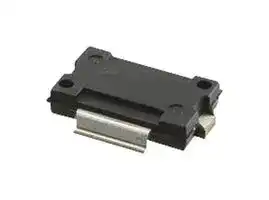
- Transistor Case Style: TO-270G
- Operating Frequency Max: 2.7GHz
- Operating Frequency Min: 1.805GHz
- Drain Source Voltage Vds: 65V
- Operating Temperature Max: 150°C
- Continuous Drain Current Id: -
| Delivery and price | |
|---|---|
| Units per pack | 50 |
| Price | 17.67 € |
| Current stock | 50+ |
| Lead time | 30 days |
**NXP Semiconductors** Technical Data Document Number: AFT20S015N Rev. 2, 04/2020 ## **RF Power LDMOS Transistors** ## N--Channel Enhancement--Mode Lateral MOSFETs These 1.5 W RF power LDMOS transistors are designed for cellular base station applications covering the frequency range of 1805 to 2700 MHz. ## **2100 MHz** - Typical Single--Carrier W--CDMA Performance: VDD = 28 Vdc, IDQ = 132 mA, Pout = 1.5 W Avg., Input Signal PAR = 9.9 dB @ 0.01% Probability on CCDF. **AFT20S015N AFT20S015GN** **1805–2700 MHz, 1.5 W AVG., 28 V AIRFAST RF POWER LDMOS TRANSISTORS** oe |**Frequency**|**Gps**<br>**(dB)**|**D**<br>**(%)**|**Output PAR**<br>**(dB)**|**ACPR**<br>**(dBc)**|**IRL**<br>**(dB)**| |---|---|---|---|---|---| |2110 MHz|17.5|22.0|8.9|--43.0|--11| |2140 MHz|17.6|22.0|9.0|--44.0|--12| |2170 MHz|17.6|22.0|9.1|--44.0|--14| **==> picture [63 x 99] intentionally omitted <==** **----- Start of picture text -----**<br> TO--270--2<br>PLASTIC<br>AFT20S015N<br>TO--270--2 GULL<br>PLASTIC<br>**----- End of picture text -----**<br> ## **1800 MHz** - Typical Single--Carrier W--CDMA Performance: VDD = 28 Vdc, IDQ = 132 mA, Pout = 1.5 W Avg., Input Signal PAR = 9.9 dB @ 0.01% Probability on CCDF. ||||**Gps**|**D**|**Output PAR**|**ACPR**|**IRL**|||||||| |---|---|---|---|---|---|---|---|---|---|---|---|---|---|---| |||**Frequency**|**(dB)**|**(%)**|**(dB)**|**(dBc)**|**(dB)**|||**TO--270--2 GULL**||||| |||1805 MHz|18.0|21.0|9.2|--42.0|--11|||||**PLASTIC**||| |||1840 MHz|18.1|22.0|9.2|--44.0|--10||||**AFT20S015GN**|||| |||||||||||||||| |||1880 MHz|18.0|22.0|9.1|--45.0|--10|||||||| |||||||||||||||| |**2600 MHz**<br><br>Typical Single--Carrier W--CDMA Performance: VDD= 28 Vdc,<br>IDQ= 132 mA, Pout= 2.1 W Avg., Input Signal PAR = 9.9 dB @ 0.01%<br>Probability on CCDF.<br>**Frequency**<br>**Gps**<br>**(dB)**<br>**D**<br>**(%)**<br>**Output PAR**<br>**(dB)**<br>**ACPR**<br>**(dBc)**<br>**IRL**<br>**(dB)**<br>2300 MHz<br>15.7<br>23.0<br>9.0<br>--45.0<br>--6<br>2400 MHz<br>16.0<br>23.0<br>8.8<br>--44.0<br>--7<br>2500 MHz<br>15.8<br>23.0<br>8.6<br>--43.0<br>--6<br>2600 MHz<br>15.8<br>21.0<br>8.5<br>--43.0<br>--7<br>2700 MHz<br>15.5<br>20.0<br>8.4<br>--42.0<br>--8<br>~~=eeues ~~|||||||||**Figure 1. Pin Connections**<br>(Top View)<br>RFout/VDS<br>RFin/VGS<br>Note: The backside of the package is the<br>source terminal for the transistor.<br> ~~a~~|||||| |**Features**||||||||||||||| ||Greater negative gate--source voltage range for improved Class C|||Greater negative gate--source voltage range for improved Class C||||||||||| ||operation|||||||||||||| (Top View) Note: The backside of the package is the source terminal for the transistor. **Figure 1. Pin Connections** - Designed for digital predistortion error correction systems - Optimized for Doherty applications 2013, 2020 NXP B.V. **AFT20S015N AFT20S015GN** RF Device Data NXP Semiconductors 1 ## **Table 1. Maximum Ratings** |**Table 1. Maximum Ratings**|**Table 1. Maximum Ratings**||||| |---|---|---|---|---|---| |**Rating**||**Symbol**|**Value**||**Unit**| |Drain--Source Voltage||VDSS|--0.5, +65||Vdc| |Gate--Source Voltage||VGS|--6.0, +10||Vdc| |Operating Voltage||VDD|32, +0||Vdc| |Storage Temperature Range||Tstg|--65 to +150||C| |Case Operating Temperature Range||TC|--40 to +150||C| |Operating Junction Temperature Range **(1,2)**||TJ|--40 to +225||C| |CW Operation @ TC= 25C<br>Derate above 25C||CW|11<br>0.1||W<br>W/C| |**Table 2. Thermal Characteristics**|||||| |**Characteristic**||**Symbol**|**Value (2,3)**||**Unit**| |Thermal Resistance, Junction to Case<br>Case Temperature 77C, 1.5 W CW, 28 Vdc, IDQ= 132 mA, 2140 MHz||RJC|4.2||C/W| |**Table 3. ESD Protection Characteristics**|||||| |**Test Methodology**|||**Class**||| |Human Body Model (per JESD22--A114)|||1C||| |Machine Model (per EIA/JESD22--A115)|||A||| |Charge Device Model (per JESD22--C101)|||IV||| |**Table 4. Moisture Sensitivity Level**|||||| |**Test Methodology**|**Rating**|**Package Peak Temperature**|||**Unit**| |Per JESD22--A113, IPC/JEDEC J--STD--020|3||260||C| |**Table 5. Electrical Characteristics** (TA= 25C unless otherwise noted)|||||| |**Characteristic**|**Symbol**|**Min**|**Typ**|**Max**|**Unit**| |**Off Characteristics**|||||| |Zero Gate Voltage Drain Leakage Current<br>(VDS= 65 Vdc, VGS= 0 Vdc)|IDSS|—|—|10|Adc| |Zero Gate Voltage Drain Leakage Current<br>(VDS= 28 Vdc, VGS= 0 Vdc)|IDSS|—|—|1|Adc| |Gate--Source Leakage Current<br>(VGS= 5 Vdc, VDS= 0 Vdc)|IGSS|—|—|1|Adc| |**On Characteristics**|||||| |Gate Threshold Voltage<br>(VDS= 10 Vdc, ID= 17.6Adc)|VGS(th)|1.5|2.0|2.5|Vdc| |Gate Quiescent Voltage<br>(VDD= 28 Vdc, ID= 132 mAdc, Measured in Functional Test)|VGS(Q)|2.4|3.0|3.4|Vdc| |Drain--Source On--Voltage<br>(VGS= 10 Vdc, ID= 176 Adc)|VDS(on)|0.1|0.2|0.3|Vdc| 1. Continuous use at maximum temperature will affect MTTF. 2. MTTF calculator available at http://www.nxp.com. 3. Refer to AN1955, _Thermal Measurement Methodology of RF Power Amplifiers._ Go to http://www.nxp.com/RF and search for AN1955. (continued) **AFT20S015N AFT20S015GN** RF Device Data NXP Semiconductors 2 **Table 5. Electrical Characteristics** (TA = 25C unless otherwise noted) **(continued)** |**Characteristic**|**Symbol**|**Min**|**Typ**|**Max**|**Unit**| |---|---|---|---|---|---| |**Functional Tests (1,2)** (In NXP Test Fixture, 50 ohm system) VDD= 28 Vdc, IDQ= 132 mA, Pout= 1.5 W Avg., f = 2170 MHz, Single--Carrier<br>W--CDMA, IQ Magnitude Clipping, Input Signal PAR = 9.9 dB @ 0.01% Probability on CCDF. ACPR measured in 3.84 MHz Channel<br>Bandwidth @5 MHz Offset.|||||| |Power Gain|Gps|16.0|17.6|19.0|dB| |Drain Efficiency|D|20.0|22.0|—|%| |Output Peak--to--Average Ratio @ 0.01% Probability on CCDF|PAR|8.6|9.1|—|dB| |Adjacent Channel Power Ratio|ACPR|—|--44.0|--41.0|dBc| |Input Return Loss|IRL|—|--14|--9|dB| |**Load Mismatch**(In NXP Test Fixture, 50 ohm system) IDQ= 132 mA, f = 2140 MHz|||||| |VSWR 10:1 at 32 Vdc, 14 W CW **(3)** Output Power<br>(3 dB Input Overdrive from 12 W CW **(3)** Rated Power)||No Device Degradation|||| |**Typical Performance**(In NXP Test Fixture, 50 ohm system) VDD= 28 Vdc, IDQ= 132 mA, 2110--2170 MHz Bandwidth|||||| |Pout@ 1 dB Compression Point, CW|P1dB|—|16.2 **(3,4)**|—|W| |AM/PM<br>(Maximum value measured at the P3dB compression point across<br>the 2110--2170 MHz frequency range.)||—|--16|—|| |VBW Resonance Point<br>(IMD Third Order Intermodulation Inflection Point)|VBWres|—|170|—|MHz| |Gain Flatness in 60 MHz Bandwidth @ Pout= 1.5 W Avg.|GF|—|0.05|—|dB| |Gain Variation over Temperature<br>(--30C to +85C)|G|—|0.01|—|dB/C| |Output Power Variation over Temperature<br>(--30C to +85C) **(3)**|P1dB|—|0.004|—|dB/C| ## **Table 6. Ordering Information** |**Device**|**Tape and Reel Information**|**Package**| |---|---|---| |AFT20S015NR1|R1 Suffix = 500 Units, 24 mm Tape Width, 13--inch Reel|TO--270--2| |AFT20S015GNR1||TO--270G--2| 1. Part internally matched on input. 2. Measurements made with device in straight lead configuration, before any lead forming operation is applied. Lead forming is used for gull wing (GN) parts. 3. Exceeds recommended operating conditions. See CW operation data in Maximum Ratings table. 4. Calculated from load pull P3dB measurements. **AFT20S015N AFT20S015GN** RF Device Data NXP Semiconductors 3 **==> picture [486 x 323] intentionally omitted <==** **----- Start of picture text -----**<br> C15<br>C27<br>C9<br>VGS D47530 C19 C21<br>VDD<br>C7<br>C23<br>C13 C11 C5*<br>C17 C25<br>C1* C2* R1 C4*<br>C3<br>R2<br>C18 C26<br>C14 C12 C6*<br>C24<br>C8<br>VDD<br>VGS C20 C22<br>C10<br>AFT20S015N<br>Rev. 2<br>C28<br>C16<br>*C1, C2, C4, C5 and C6 are mounted vertically.<br>Note: NXP has begun the transition of marking printed circuit boards (PCBs) with the NXP exception logo. PCBs may have either Freescale<br>or NXP markings during the transition period. These changes will have no impact on form, fit or function of the current product.<br>CUT OUT AREA<br>**----- End of picture text -----**<br> **Figure 2. AFT20S015N Test Circuit Component Layout — 2110--2170 MHz** **Table 7. AFT20S015N Test Circuit Component Designations and Values — 2110--2170 MHz** |**Part**|**Description**|**Part Number**|**Manufacturer**| |---|---|---|---| |C1|8.2 pF Chip Capacitor|ATC100B8R2CT500XT|ATC| |C2|2.4 pF Chip Capacitor|ATC800B2R4BT500XT|ATC| |C3|1.7 pF Chip Capacitor|ATC100B1R7BT500XT|ATC| |C4|9.1 pF Chip Capacitor|ATC100B9R1CT500XT|ATC| |C5, C6|6.8 pF Chip Capacitors|ATC100B6R8CT500XT|ATC| |C7, C8|240 pF Chip Capacitors|ATC100B241JT200XT|ATC| |C9, C10, C21, C22|220 pF Chip Capacitors|C1812C224K5RAC--TU|Kemet| |C11, C12, C23, C24|<br>0.1F Chip Capacitors|CDR33BX104AKWS|AVX| |C13, C14, C25, C26|<br>2.2F Chip Capacitors|C1825C225J5RAC--TU|Kemet| |C15, C16|22F, 35 V Tantalum Capacitors|T491X226K035AT|Kemet| |C17, C18, C19, C20|<br>75 pF Chip Capacitors|ATC800B750JT500XT|ATC| |C27, C28|470 F, 63 V Electrolytic Capacitors|MCGPR63V477M13X26--RH|Multicomp| |R1, R2|1Chip Resistors|CRCW12061R00FKEA|Vishay| |PCB|Rogers RO4350B, 0.020,r = 3.66|D47530|MTL| **AFT20S015N AFT20S015GN** RF Device Data NXP Semiconductors 4 ## **TYPICAL CHARACTERISTICS — 2110--2170 MHZ** **==> picture [402 x 617] intentionally omitted <==** **----- Start of picture text -----**<br> 18 23<br>VDD = 28 Vdc, Pout = 1.5 W (Avg.)<br>17.9 D IDQ = 132 mA, Single--Carrier W--CDMA 22.5<br>17.8 22<br>17.7 21.5<br>Gps<br>17.6 21<br>17.5 --41 --9 --0.4<br>IRL<br>17.4 PARC --42 --13 --0.6<br>17.3 --43 --17 --0.8<br>ACPR<br>17.2 --44 --21 --1<br>17.1 3.84 MHz Channel Bandwidth --45 --25 --1.2<br>Input Signal PAR = 9.9 dB @ 0.01% Probability on CCDF<br>17 --46 --29 --1.4<br>2060 2080 2100 2120 2140 2160 2180 2200 2220<br>f, FREQUENCY (MHz)<br>Figure 3. Single--Carrier Output Peak--to--Average Ratio Compression<br>(PARC) Broadband Performance @ Pout = 1.5 Watts Avg.<br>--10<br>VDD = 28 Vdc, Pout = 10 W (PEP), IDQ = 132 mA<br>Two--Tone Measurements, (f1 + f2)/2 = Center<br>--20 Frequency of 2140 MHz<br>IM3--U<br>--30 IM3--L<br>IM5--U<br>--40 IM5--L<br>IM7--U<br>--50<br>IM7--L<br>--60<br>1 10 100 200<br>TWO--TONE SPACING (MHz)<br>Figure 4. Intermodulation Distortion Products<br>versus Two--Tone Spacing<br>18.5 0 60 --25<br>--1 dB = 1.5 W<br>ACPR<br>18 --1 50 --30<br>--2 dB = 2.2 W D<br>17.5 --2 40 --35<br>Gps<br>17 --3 30 --40<br>16.5 --4 --3 dB = 3 W 20 --45<br>PARC<br>16 --5 VDD = 28 Vdc, IDQ = 132 mA, f = 2140 MHz 10 --50<br>Single--Carrier W--CDMA, 3.84 MHz Channel Bandwidth<br>Input Signal PAR = 9.9 dB @ 0.01% Probability on CCDF<br>15.5 --6 0 --55<br>1 2 3 4 5 6<br>Pout, OUTPUT POWER (WATTS)<br>, DRAIN<br>D<br><br>EFFICIENCY (%)<br>, POWER GAIN (dB)<br>ps<br>G<br>ACPR (dBc) PARC (dB)<br>IRL, INPUT RETURN LOSS (dB)<br>IMD, INTERMODULATION DISTORTION (dBc)<br>ACPR (dBc)<br>, POWER GAIN (dB) DRAIN EFFICIENCY (%)<br>Gps D<br><br>PROBABILITY ON CCDF (dB)<br>OUTPUT COMPRESSION AT 0.01%<br>**----- End of picture text -----**<br> **Figure 5. Output Peak--to--Average Ratio Compression (PARC) versus Output Power** **AFT20S015N AFT20S015GN** RF Device Data NXP Semiconductors 5 ## **TYPICAL CHARACTERISTICS — 2110--2170 MHz** **==> picture [292 x 159] intentionally omitted <==** **----- Start of picture text -----**<br> 20 60 0<br>VDD = 28 Vdc, IDQ = 132 mA 2140 MHz<br>Single--Carrier W--CDMA 2110 MHz<br>19 D 50 --10<br>2140 MHz 2170 MHz 2170 MHz<br>18 Gps 40 --20<br>ACPR<br>17 30 --30<br>2110 MHz<br>2170 MHz<br>16 20 --40<br>2140 MHz<br>2110 MHz<br>15 10 --50<br>3.84 MHz Channel Bandwidth, Input Signal<br>PAR = 9.9 dB @ 0.01% Probability on CCDF<br>14 0 --60<br>1 10 20<br>, POWER GAIN (dB) ACPR (dBc)<br>ps<br>G , DRAIN EFFICIENCY (%)<br>D<br><br>**----- End of picture text -----**<br> **==> picture [116 x 8] intentionally omitted <==** **----- Start of picture text -----**<br> Pout, OUTPUT POWER (WATTS) AVG.<br>**----- End of picture text -----**<br> **Figure 6. Single--Carrier W--CDMA Power Gain, Drain Efficiency and ACPR versus Output Power** **==> picture [256 x 173] intentionally omitted <==** **----- Start of picture text -----**<br> 21 20<br>VDD = 28 Vdc<br>19 P in = 0 dBm 10<br>IDQ = 132 mA Gain<br>17 0<br>15 --10<br>13 --20<br>IRL<br>11 --30<br>9 --40<br>1700 1800 1900 2000 2100 2200 2300 2400 2500<br>f, FREQUENCY (MHz)<br>GAIN (dB) IRL (dB)<br>**----- End of picture text -----**<br> **Figure 7. Broadband Frequency Response** **AFT20S015N AFT20S015GN** RF Device Data NXP Semiconductors 6 **ALTERNATE CHARACTERIZATION — 1805--1880 MHz** **==> picture [486 x 323] intentionally omitted <==** **----- Start of picture text -----**<br> C16<br>C28<br>C10<br>VGS D45064 C20<br>C8 VDD<br>C14 C12 C6*<br>C18 C22 [C24] C26<br>C1* C2* R1 C4*<br>C3*<br>R2 C5*<br>C19 C23 C25 C27<br>C15 C13 C7*<br>C9 VDD<br>VGS C21<br>C11<br>AFT20S015N<br>Rev. 2<br>C29<br>C17<br>*C1, C2, C3, C4, C5, C6 and C7 are mounted vertically.<br>Note: NXP has begun the transition of marking printed circuit boards (PCBs) with the NXP exception logo. PCBs may have either Freescale<br>or NXP markings during the transition period. These changes will have no impact on form, fit or function of the current product.<br>CUT OUT AREA<br>**----- End of picture text -----**<br> **Figure 8. AFT20S015N Test Circuit Component Layout — 1805--1880 MHz** **Table 8. AFT20S015N Test Circuit Component Designations and Values — 1805--1880 MHz** |**Part**|**Description**|**Part Number**|**Manufacturer**| |---|---|---|---| |C1|11 pF Chip Capacitor|ATC100B11R0CT500XT|ATC| |C2, C3|3.3 pF Chip Capacitors|ATC800B3R3BT500XT|ATC| |C4, C5|47 pF Chip Capacitors|ATC600F47BT250XT|ATC| |C6, C7|6.8 pF Chip Capacitors|ATC100B6R8CT500XT|ATC| |C8, C9|240 pF Chip Capacitors|ATC100B241JT200XT|ATC| |C10, C11, C22, C|23<br>220 pF Chip Capacitors|C1812C224K5RAC--TU|Kemet| |C12, C13, C24, C|25<br>0.1F Chip Capacitors|CDR33BX104AKWS|AVX| |C14, C15, C26, C|27<br>2.2F, 50 V Chip Capacitors|C1825C225J5RAC--TU|Kemet| |C16, C17|22F, 35 V Tantalum Capacitors|T491X226K035AT|Kemet| |C18, C19, C20, C|21<br>75 pF Chip Capacitors|ATC800B750JT500XT|ATC| |C28, C29|470F, 63 V Electrolytic Capacitors|MCGPR63V477M13X26--RH|Multicomp| |R1, R2|1Chip Resistors|CRCW12061R00FKEA|Vishay| |PCB|Rogers RO4350B, 0.020,r = 3.66|D45064|MTL| **AFT20S015N AFT20S015GN** RF Device Data NXP Semiconductors 7 ## **ALTERNATE CHARACTERIZATION — 1805--1880 MHz** **==> picture [357 x 612] intentionally omitted <==** **----- Start of picture text -----**<br> 19 23<br>18.8 22<br>D<br>18.6 VDD = 28 Vdc, Pout = 1.5 W (Avg.) 21<br>18.4 IDQ = 132 mA, Single--Carrier W--CDMA 20<br>3.84 MHz Channel Bandwidth, Input Signal<br>18.2 Gps PAR = 9.9 dB @ 0.01% Probability on CCDF 19<br>18 --41 --9 --0.3<br>ACPR<br>17.8 --42 --9.5 --0.4<br>17.6 --43 --10 --0.5<br>PARC<br>17.4 --44 --10.5 --0.6<br>17.2 IRL --45 --11 --0.7<br>17 --46 --11.5 --0.8<br>1760 1780 1800 1820 1840 1860 1880 1900 1920<br>f, FREQUENCY (MHz)<br>Figure 9. Single--Carrier Output Peak--to--Average Ratio Compression<br>(PARC) Broadband Performance @ Pout = 1.5 Watts Avg.out = 1.5 Watts Avg. = 1.5 Watts Avg.<br>18.4 30 --25<br>VDD = 28 Vdc, IDQ = 132 mA 1805 MHz<br>Single--Carrier W--CDMA 1840 MHz<br>18.3 3.84 MHz Channel Bandwidth D 25 --30<br>1880 MHz<br>1840 MHz<br>18.2 20 --35<br>18.1 Gps ACPR 15 --40<br>1805 MHz<br>18 1880 MHz 10 --45<br>1880 MHz<br>17.9 1805 MHz 5 --50<br>1840 MHz<br>17.8 Input Signal PAR = 9.9 dB @ 0.01% Probability on CCDF 0 --55<br>0.1 1 5<br>Pout, OUTPUT POWER (WATTS) AVG.<br>Figure 10. Single--Carrier W--CDMA Power Gain, Drain<br>Efficiency and ACPR versus Output Power<br>21 0<br>VDD = 28 Vdc<br>19 P in = 0 dBm Gain --2<br>IDQ = 132 mA<br>17 --4<br>15 --6<br>13 --8<br>IRL<br>11 --10<br>9 --12<br>1400 1500 1600 1700 1800 1900 2000 2100 2200<br>f, FREQUENCY (MHz)<br>, DRAIN<br>D<br><br>EFFICIENCY (%)<br>, POWER GAIN (dB)<br>ps<br>G<br>ACPR (dBc) PARC (dB)<br>IRL, INPUT RETURN LOSS (dB)<br>, POWER GAIN (dB) ACPR (dBc)<br>ps<br>G , DRAIN EFFICIENCY (%)<br>D<br><br>GAIN (dB) IRL (dB)<br>**----- End of picture text -----**<br> **Figure 9. Single--Carrier Output Peak--to--Average Ratio Compression (PARC) Broadband Performance @ Pout = 1.5 Watts Avg.out = 1.5 Watts Avg. = 1.5 Watts Avg.** **Figure 11. Broadband Frequency Response** **AFT20S015N AFT20S015GN** RF Device Data NXP Semiconductors 8 **ALTERNATE CHARACTERIZATION — 2300--2700 MHz** **==> picture [487 x 322] intentionally omitted <==** **----- Start of picture text -----**<br> C15 C20<br>C9<br>VGS D48048 C18 C19<br>C7 VDD<br>C13 C11<br>C5<br>C4* C17 C21<br>C1* C2* C3*<br>R1<br>R2<br>C14 C12 C6<br>C8 VDD<br>VGS<br>C10<br>AFT20S015N 2.6 GHz<br>Rev. 0<br>C16<br>*C1, C2, C3 and C4 are mounted vertically.<br>Note: NXP has begun the transition of marking printed circuit boards (PCBs) with the NXP exception logo. PCBs may have either Freescale<br>or NXP markings during the transition period. These changes will have no impact on form, fit or function of the current product.<br>CUT OUT AREA<br>**----- End of picture text -----**<br> **Figure 12. AFT20S015N Test Circuit Component Layout — 2300--2700 MHz** **Table 9. AFT20S015N Test Circuit Component Designations and Values — 2300--2700 MHz** |**Part**|**Description**|**Part Number**|**Manufacturer**| |---|---|---|---| |C1|4.3 pF Chip Capacitor|ATC600F4R3CT250XT|ATC| |C2|1.3 pF Chip Capacitor|ATC800B1R3BT500XT|ATC| |C3|8.2 pF Chip Capacitor|ATC600F8R2BT250XT|ATC| |C4|6.8 pF Chip Capacitor|ATC100B6R8CT500XT|ATC| |C5, C6|6.8 pF Chip Capacitors|ATC800B6R8CT500XT|ATC| |C7, C8, C17|2.2F Chip Capacitors|C3225X7R1H225KT|TDK| |C9, C10, C18|220 nF Chip Capacitors|C1812C224K5RAC--TU|Kemet| |C11, C12, C19|0.1F Chip Capacitors|CDR33BX104AKWS|AVX| |C13, C14, C21|2.2F Chip Capacitors|C1825C225J5RAC--TU|Kemet| |C15, C16|22 F, 35 V Tantalum Capacitors|T491X226K035AT|Kemet| |C20|470F, 63 V Electrolytic Capacitor|MCGPR63V477M13X26--RH|Multicomp| |R1, R2|4.75Chip Resistors|CRCW12064R75FKEA|Vishay| |PCB|Rogers RO4350B, 0.020,r = 3.66|D48048|MTL| **AFT20S015N AFT20S015GN** RF Device Data NXP Semiconductors 9 ## **ALTERNATE CHARACTERIZATION — 2300--2700 MHz** **==> picture [351 x 394] intentionally omitted <==** **----- Start of picture text -----**<br> 17.5 25<br>VDD = 28 Vdc, Pout = 2.1 W (Avg.)<br>17 23<br>D IDQ = 132 mA<br>16.5 21<br>16 Gps 19<br>15.5 17<br>Single--Carrier W--CDMA 3.84 MHz Channel<br>15 --39 0 --0.6<br>Bandwidth, Input Signal PAR = 9.9 dB @<br>14.5 0.01% Probability on CCDF ACPR --41 --2 --0.8<br>14 --43 --4 --1<br>13.5 IRL --45 --6 --1.2<br>13 --47 --8 --1.4<br>PARC<br>12.5 --49 --10 --1.6<br>2200 2275 2350 2425 2500 2575 2650 2725 2800<br>f, FREQUENCY (MHz)<br>Figure 13. Single--Carrier Output Peak--to--Average Ratio Compression<br>(PARC) Broadband Performance @ Pout = 2.1 Watts Avg.out = 2.1 Watts Avg. = 2.1 Watts Avg.<br>16.2 30 --25<br>VDD = 28 Vdc, IDQ = 132 mA 2300 MHz<br>Single--Carrier W--CDMA<br>16 3.84 MHz Channel Bandwidth 2500 MHz D 25 --30<br>2700 MHz<br>15.8 20 --35<br>15.6 Gps 15 --40<br>2300 MHz 2500 MHz<br>15.4 10 --45<br>2700 MHz<br>15.2 2300 MHz 5 --50<br>ACPR<br>2700 MHz 2500 MHz<br>15 Input Signal PAR = 9.9 dB @ 0.01% Probability on CCDF 0 --55<br>0.1 1 5<br>Pout, OUTPUT POWER (WATTS) AVG.<br>, DRAIN<br>D<br><br>EFFICIENCY (%)<br>, POWER GAIN (dB)<br>ps<br>G<br>ACPR (dBc) PARC (dB)<br>IRL, INPUT RETURN LOSS (dB)<br>, POWER GAIN (dB) ACPR (dBc)<br>ps<br>G , DRAIN EFFICIENCY (%)<br>D<br><br>**----- End of picture text -----**<br> **Figure 13. Single--Carrier Output Peak--to--Average Ratio Compression (PARC) Broadband Performance @ Pout = 2.1 Watts Avg.out = 2.1 Watts Avg. = 2.1 Watts Avg.** **Figure 14. Single--Carrier W--CDMA Power Gain, Drain Efficiency and ACPR versus Output Power** **==> picture [256 x 174] intentionally omitted <==** **----- Start of picture text -----**<br> 21 2<br>VDD = 28 Vdc<br>19 P in = 0 dBm 0<br>IDQ = 132 mA<br>17 --2<br>Gain<br>15 --4<br>13 --6<br>IRL<br>11 --8<br>9 --10<br>2100 2250 2400 2550 2700 2850 3000 3150 3300<br>f, FREQUENCY (MHz)<br>GAIN (dB) IRL (dB)<br>**----- End of picture text -----**<br> **Figure 15. Broadband Frequency Response** **AFT20S015N AFT20S015GN** RF Device Data NXP Semiconductors 10 ## **PACKAGE INFORMATION** **AFT20S015N AFT20S015GN** RF Device Data NXP Semiconductors 11 **AFT20S015N AFT20S015GN** RF Device Data NXP Semiconductors 12 **==> picture [502 x 204] intentionally omitted <==** **AFT20S015N AFT20S015GN** RF Device Data NXP Semiconductors 13 **AFT20S015N AFT20S015GN** RF Device Data NXP Semiconductors 14 **AFT20S015N AFT20S015GN** RF Device Data NXP Semiconductors 15 **==> picture [502 x 230] intentionally omitted <==** **AFT20S015N AFT20S015GN** RF Device Data NXP Semiconductors 16 ## **PRODUCT DOCUMENTATION, SOFTWARE AND TOOLS** Refer to the following documents, software and tools to aid your design process. ## **Application Notes** - AN1907: Solder Reflow Attach Method for High Power RF Devices in Plastic Packages - AN1955: Thermal Measurement Methodology of RF Power Amplifiers - AN3789: Clamping of High Power RF Transistors and RFICs in Over--Molded Plastic Packages ## **Software** - Electromigration MTTF Calculator - RF High Power Model - .s2p File ## **Development Tools** - Printed Circuit Boards ## **REVISION HISTORY** The following table summarizes revisions to this document. |**Revision**|**Date**|**Description**| |---|---|---| |0|Apr. 2013|<br>Initial Release of Data Sheet| |1|Nov. 2013|<br>Upper frequency limit changed from 2690 to 2700 MHz to reflect measurement data, p. 1<br><br>Table 2, Thermal Characteristics: changed 2170 to 2140 MHz to reflect recent thermal test results, p. 2<br><br>Table 5, Electrical Characteristics, Load Mismatch: updated VSWR power levels (8 W CW to 14 W CW,<br>7 W CW to 12 W CW) to reflect recent characterization data test results, p. 3<br><br>Table 5, Electrical Characteristics, Typical Performance: changed P1dB from 7 W to 16.2 W based on<br>P3dB load pull calculations, p. 3<br><br>Figs. 2, 8, 12, Test Circuit Component Layout: added MTL number, pp. 4, 7, 9<br>Tables 6, 7, 8, Test Circuit Component Designations and Values: updated PCB description to reflect most<br>current board specifications from Rogers and added MTL part number, pp. 4, 7, 9| |2|Apr. 2020|<br>Package Outline Drawings: TO–270–2 package outline updated to Rev. R, pp. 11–13. TO–270G–2<br>package outline updated to Rev. D, pp. 14–16.<br><br>General updates made to align data sheet to current standard| **AFT20S015N AFT20S015GN** RF Device Data NXP Semiconductors 17 **==> picture [506 x 36] intentionally omitted <==** ## _**How to Reach Us:**_ **Home Page:** nxp.com **Web Support:** nxp.com/support Information in this document is provided solely to enable system and software implementers to use NXP products. There are no express or implied copyright licenses granted hereunder to design or fabricate any integrated circuits based on the information in this document. NXP reserves the right to make changes without further notice to any products herein. NXP makes no warranty, representation, or guarantee regarding the suitability of its products for any particular purpose, nor does NXP assume any liability arising out of the application or use of any product or circuit, and specifically disclaims any and all liability, including without limitation consequential or incidental damages. “Typical” parameters that may be provided in NXP data sheets and/or specifications can and do vary in different applications, and actual performance may vary over time. All operating parameters, including “typicals,” must be validated for each customer application by customer’s technical experts. NXP does not convey any license under its patent rights nor the rights of others. NXP sells products pursuant to standard terms and conditions of sale, which can be found at the following address: nxp.com/SalesTermsandConditions. NXP, the NXP logo, Freescale, the Freescale logo and Airfast are trademarks of NXP B.V. All other product or service names are the property of their respective owners. E 2013, 2020 NXP B.V. **AFT20S015N AFT20S015GN** **==> picture [112 x 37] intentionally omitted <==** RF Device Data NXP Semiconductors Document Number: AFT20S015N 18Rev. 2, 04/2020
Updated at April 10, 2026
NXP Semiconductors is a global leader in secure connectivity solutions, driving innovation across the automotive, industrial, IoT, mobile, and communications infrastructure markets. By developing advanced, purpose-built technologies, NXP enables devices to sense, think, connect, and act intelligently, delivering rigorously tested components that make the connected world safer and more efficient. Within the semiconductor space, NXP is highly regarded for its extensive range of high-performance integrated circuits and discrete devices. The brand's portfolio excels in drivers and interfaces, featuring a comprehensive selection of I/O expanders designed to streamline complex system architectures. For demanding high-frequency and wireless applications, NXP provides industry-leading RF FETs and RF/PIN diodes engineered to deliver exceptional signal integrity, efficiency, and reliability. The NXP product lineup further extends to essential discrete components, including versatile bipolar transistors, JFETs, and small signal diodes optimized for precision switching and amplification. Additionally, the portfolio supports advanced automation and smart applications with precision IC sensors, such as MEMS accelerometers, alongside specialized power management solutions like AC/DC LED driver ICs and single MOSFETs for cutting-edge electronics design.
About Novapart
Novapart is a B2B electronic component broker specialising in stock shortages and cost reduction. We source hard-to-find parts and identify compliant alternatives across a catalogue of 540,000+ components from 500+ manufacturers.
Learn more →Stock Shortage Specialist
When a component is unavailable, discontinued or has an unacceptable lead time, we tap into our network of vetted European and Asian distributors to source what you need — without compromising on quality or traceability.
Request a quote →Compliant Alternatives
We identify pin-to-pin, electrically equivalent substitutes that meet the same certifications (RoHS, AEC-Q100, REACH) as your original specification — validated against datasheets, not just part numbers. Often at a lower cost.
BOM Analysis service →