
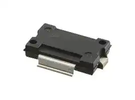


AFT05MS031GNR1
RF FET Transistor, 40 V, 294 W, 136 MHz, 520 MHz, TO-270
- Manufacturer: NXP
- Product type: RF FETs
- Drain Source Voltage Vds:40V; Continuous Drain Current Id:-; Power Dissipation Pd:294W; Operating Frequency Min:136MHz; Operating Frequency Max:520MHz; RF Transistor Case:TO-270; No. o
- MSL: MSL 3 - 168 hours
- SVHC: No SVHC (27-Jun-2024)
- No. of Pins: 2Pins
- Channel Type: N Channel
- Product Range: AFT05MS031GN
- Power Dissipation: 294W
- Transistor Mounting: Surface Mount
- Transistor Case Style: TO-270
- Operating Frequency Max: 520MHz
- Operating Frequency Min: 136MHz
- Drain Source Voltage Vds: 40V
- Operating Temperature Max: 150°C
- Continuous Drain Current Id: -
| Delivery and price | |
|---|---|
| Units per pack | 500 |
| Price | 10.58 € |
| Current stock | 10+ |
| Lead time | 30 days |
**Freescale Semiconductor** Technical Data
Document Number: AFT05MS031N Rev. 1, 4/2013
## **RF Power LDMOS Transistors** High Ruggedness N--Channel Enhancement--Mode Lateral MOSFETs
Designed for mobile two--way radio applications with frequencies from 136 to 520 MHz. The high gain, ruggedness and broadband performance of these devices make them ideal for large--signal, common source amplifier applications in mobile radio equipment.
## **Typical Performance:** (13.6 Vdc, TA = 25C, CW)
|**Frequency**<br>**(MHz)**|**Gps**<br>**(dB)**|**D**<br>**(%)**|**P1dB**<br>**(W)**|
|---|---|---|---|
|136--174 **(1,4)**|23.2|62.0|31|
|380--450 **(2,4)**|18.3|64.1|31|
|450--520 **(3,4)**|17.7|62.0|31|
|520 **(5)**|17.7|71.4|33|
## **Load Mismatch/Ruggedness**
|**Frequency**<br>**(MHz)**|**Signal**<br>**Type**|**VSWR**|**Pin**<br>**(W)**|**Test**<br>**Voltage**|**Result**|
|---|---|---|---|---|---|
|155 **(1)**|CW|>65:1 at all<br>Phase Angles|0.55<br>(3 dB Overdrive)|17|No Device<br>Degradation|
|420 **(2)**|||1.6<br>(3 dB Overdrive)|||
|490 **(3)**|||2.0<br>(3 dB Overdrive)|||
|520 **(5)**|||1.1<br>(3 dB Overdrive)|||
## **AFT05MS031NR1 AFT05MS031GNR1** ~~a~~
**136--520 MHz, 31 W, 13.6 V WIDEBAND RF POWER LDMOS TRANSISTORS**
**==> picture [73 x 112] intentionally omitted <==**
**----- Start of picture text -----**<br>
TO--270--2<br>PLASTIC<br>AFT05MS031NR1<br>TO--270--2 GULL<br>PLASTIC<br>AFT05MS031GNR1<br>**----- End of picture text -----**<br>
1. Measured in 136--174 MHz VHF broadband reference circuit.
2. Measured in 380--450 MHz UHF broadband reference circuit.
3. Measured in 450--520 MHz UHF broadband reference circuit.
4. The values shown are the minimum measured performance numbers across the indicated frequency range.
5. Measured in 520 MHz narrowband test circuit.
## **Features**
- Characterized for Operation from 136 to 520 MHz
- Unmatched Input and Output Allowing Wide Frequency Range Utilization
- Integrated ESD Protection
**==> picture [155 x 94] intentionally omitted <==**
**----- Start of picture text -----**<br>
Gate Drain<br>| __|<br>(Top View)<br>Note: The backside of the package is the<br>source terminal for the transistor.<br>**----- End of picture text -----**<br>
- Integrated Stability Enhancements
- Wideband — Full Power Across the Band:
**Figure 1. Pin Connections**
- 136--174 MHz
- 380--450 MHz
- 450--520 MHz
- 225C Capable Plastic Package
- Exceptional Thermal Performance
- High Linearity for: TETRA, SSB, LTE
- Cost--effective Over--molded Plastic Packaging
- In Tape and Reel. R1 Suffix = 500 Units, 24 mm Tape Width, 13 inch Reel.
## **Typical Applications**
- Output Stage VHF Band Mobile Radio
- Output Stage UHF Band Mobile Radio
Freescale Semiconductor, Inc., 2012--2013. All rights reserved. **AFT05MS031NR1 AFT05MS031GNR1** ~~a = freescale~~
**AFT05MS031NR1 AFT05MS031GNR1** Airfast 1
RF Device Data Freescale Semiconductor, Inc.
## **Table 1. Maximum Ratings**
|**Table 1. Maximum Ratings**||||||
|---|---|---|---|---|---|
|**Rating**|||**Symbol**<br>**Value**||**Unit**|
|Drain--Source Voltage|||VDSS<br>--0.5, +40||Vdc|
|Gate--Source Voltage|||VGS<br>--6.0, +12||Vdc|
|Operating Voltage|||VDD<br>17, +0||Vdc|
|Storage Temperature Range|||Tstg<br>--65 to +150||C|
|Case Operating Temperature Range|||TC<br>--40 to +150||C|
|Operating Junction Temperature Range **(1,2)**|||TJ<br>--40 to +225||C|
|Total Device Dissipation @ TC= 25C|||PD<br>294||W|
|Derate above 25C|||1.47||W/C|
|**Table 2. Thermal Characteristics**||||||
|**Characteristic**<br>**Symbol**<br>**Value (2,3)**<br>**Unit**<br>Thermal Resistance, Junction to Case<br>Case Temperature 79C, 31 W CW, 13.6 Vdc, IDQ= 10 mA, 520 MHz<br>RJC<br>0.67<br>C/W<br>~~I~~||||||
|**Table 3. ESD Protection Characteristics**||||||
|**Test Methodology**<br>**Class**<br>Human Body Model (per JESD22--A114)<br>2, passes 2500 V<br>Machine Model (per EIA/JESD22--A115)<br>A, passes 100 V<br>Charge Device Model (per JESD22--C101)<br>IV, passes 2000 V<br>**Table 4. Moisture Sensitivity Level**<br>**Test Methodology**<br>**Rating**<br>**Package Peak Temperature**<br>**Unit**<br>Per JESD22--A113, IPC/JEDEC J--STD--020<br>3<br>260<br>C<br>~~a~~||||||
|**Table 5. Electrical Characteristics** (TA= 25C unless otherwise noted)||||||
|**Characteristic**||**Symbol**|**Min**<br>**Typ**<br>**Max**||**Unit**|
|**Off Characteristics**||||||
|Zero Gate Voltage Drain Leakage Current<br>(VDS= 40 Vdc, VGS= 0 Vdc)<br>IDSS<br>—<br>—<br>2<br>Adc<br>Zero Gate Voltage Drain Leakage Current<br>(VDS= 13.6 Vdc, VGS= 0 Vdc)<br>IDSS<br>—<br>—<br>1<br>Adc<br>Gate--Source Leakage Current<br>(VGS= 5 Vdc, VDS= 0 Vdc)<br>IGSS<br>—<br>—<br>600<br>nAdc<br>~~pr~~||||||
|**On Characteristics**||||||
|Gate Threshold Voltage<br>(VDS= 10 Vdc, ID= 115Adc)<br>VGS(th)<br>1.6<br>2.1<br>2.6<br>Vdc<br>Drain--Source On--Voltage<br>(VGS= 10 Vdc, ID= 1.2 Adc)<br>VDS(on)<br>—<br>0.13<br>—<br>Vdc<br>Forward Transconductance<br>(VDS= 10 Vdc, ID= 7.5 Adc)<br>gfs<br>—<br>5.8<br>—<br>S<br>~~ae~~||||||
|1. Continuous use at maximum temperature will affect MTTF.||||||
|2. MTTF calculator available athttp://www.freescale.com/rf<br>.Select Software & Tools/Development Tools/Calculators to access MTTF||||||
|calculators by product.||||||
3. Refer to AN1955, _Thermal Measurement Methodology of RF Power Amplifiers._ Go to http://www.freescale.com/rf. Select Documentation/Application Notes -- AN1955.
(continued)
**AFT05MS031NR1 AFT05MS031GNR1**
RF Device Data Freescale Semiconductor, Inc.
2
**Table 5. Electrical Characteristics** (TA = 25C unless otherwise noted) **(continued)**
|**Table 5. Electrical Characteristics** (TA = 25C unless otherwise noted)A = 25C unless otherwise noted)= 25C unless otherwise noted)C unless otherwise noted)C unless otherwise noted)**(continued)**|**(continued)**|**(continued)**|
|---|---|---|
|**Characteristic**<br>**Symbol**||**Min**<br>**Typ**<br>**Max**<br>**Unit**|
|**Dynamic Characteristics**|||
|Reverse Transfer Capacitance<br>Crss||—<br>1.6<br>—<br>pF|
|(VDS= 13.6 Vdc30 mV(rms)ac @ 1 MHz, VGS= 0 Vdc)|||
|Output Capacitance<br>Coss||—<br>49.5<br>—<br>pF|
|(VDS= 13.6 Vdc30 mV(rms)ac @ 1 MHz, VGS= 0 Vdc)|||
|Input Capacitance<br>Ciss||—<br>109<br>—<br>pF|
|(VDS= 13.6 Vdc, VGS= 0 Vdc30 mV(rms)ac @ 1 MHz)<br>**Functional Tests (1)** (In Freescale Narrowband Test Fixture, 50 ohm system) VDD= 13.6 Vdc, IDQ= 10 mA, Pout= 31 W, f = 520 MHz<br>Common--Source Amplifier Power Gain<br>Gps<br>16.5<br>17.7<br>19.0<br>dB<br>Drain Efficiency<br>D<br>70.0<br>71.4<br>—<br>%<br>**Load Mismatch/Ruggedness**(In Freescale Test Fixture, 50 ohm system) IDQ= 10 mA<br>**Frequency**<br>**(MHz)**<br>**Signal**<br>**Type**<br>**VSWR**<br>**Pin**<br>**(W)**<br>**Test Voltage, VDD**<br>**Result**<br>520<br>CW<br>>65:1 at all Phase Angles<br>1.1<br>(3 dB Overdrive)<br>17<br>No Device Degradation<br>~~_—————~~<br>~~ee~~<br>~~a~~|||
|1. Measurements made with device in straight lead configuration before any lead forming operation is applied. Lead forming is used for gull|||
|wing (GN) parts.|||
**AFT05MS031NR1 AFT05MS031GNR1**
RF Device Data Freescale Semiconductor, Inc.
3
## **TYPICAL CHARACTERISTICS**
**==> picture [238 x 174] intentionally omitted <==**
**----- Start of picture text -----**<br>
1000<br>a Measured with 30 mV(rms)ac @ 1 MHz, VGS = 0 Vdc<br>Ciss<br>100<br>—<———————————————————ee Coss<br>10 a a ee eee<br>a ee es ee<br>a Crss<br>1<br>0 4 8 12 16 20<br>VDS, DRAIN--SOURCE VOLTAGE (VOLTS)<br>C, CAPACITANCE (pF)<br>**----- End of picture text -----**<br>
**Figure 2. Capacitance versus Drain--Source Voltage**
**==> picture [235 x 175] intentionally omitted <==**
**----- Start of picture text -----**<br>
7<br>ee TA = 25C VGS = 4.25 Vdc<br>6 ———<br>45 SS el 4 Vdc<br>3.75 Vdc<br>3<br>3.5 Vdc<br>Y/<br>2<br>3.25 Vdc<br>1<br>2.75 Vdc 3 Vdc<br>0<br>0 4 8 12 16 20<br>VDS, DRAIN--SOURCE VOLTAGE (VOLTS)<br>, DRAIN CURRENT (AMPS)<br>IDS<br>**----- End of picture text -----**<br>
**Figure 3. Drain Current versus Drain--Source Voltage**
**==> picture [239 x 233] intentionally omitted <==**
**----- Start of picture text -----**<br>
10 [9]<br>=== === = SS SS<br>i<br>VDD = 13.6 Vdc<br>10 [8] | ft | ff td ff<br>ID = 2.5 Amps<br>SSZ7™-.N aEee eee eS<br>10 [7] 3.2 Amps<br>LSS ee, EL<br>pf ESS Ht HT<br>10 [6]<br>pj | | | | Se td<br>3.9 Amps<br>a ee ee a<br>10 [5]<br>ptt ft ff | td<br>SSSee<br>ee<br>10 [4] Pp tt | | te te tt tT tT Tt ee ee ee<br>90 110 130 150 170 190 210 230 250<br>TJ, JUNCTION TEMPERATURE (C)<br>Note: MTTF value represents the total cumulative operating time<br>under indicated test conditions.<br>MTTF calculator available at http://www.freescale.com/rf. Select<br>Software & Tools/Development Tools/Calculators to access MTTF<br>calculators by product.<br>MTTF (HOURS)<br>**----- End of picture text -----**<br>
**Figure 4. MTTF versus Junction Temperature -- CW**
**AFT05MS031NR1 AFT05MS031GNR1**
RF Device Data Freescale Semiconductor, Inc.
4
**520 MHz NARROWBAND PRODUCTION TEST FIXTURE**
**==> picture [474 x 181] intentionally omitted <==**
**----- Start of picture text -----**<br>
C1<br>C7 C13 C14<br>© , an ccce% 0000000, £ £ o aap pooceSbooc0000000%<br>° EI ° of KH °<br>o| | ° ° B3 Ld °<br>°° C3 B1 g C16 in B2 °<br>o}oL IpTt] LL 4 °° @ ) B s 8 °°<br>® 0 C2 6600000000 C4 0 0 ° laa: C8 ° ° a | ° o000000 C18 [ 500 ®<br>C5 ° ° = °\/° C9 O09 O0000}° |, L2 °° C11<br>©00 0 /000000000 0 000 L1 =) YY C15 ©00000000000\00000<br>C T T a = ‘J<br>e s | | oO [4<br>000050000000 000000 CL I S) ©0000000000000<br>C6 00000000 C10 0000 00000002 C12 °°°°°<br>°°<br>°<br>><a“ee2 ® ® O o05000 —_R Rs°<br>=" f reescale”semiconductor (4 ) AFT05MS031N C17 @<br>Rev. 1<br>CUT OUT AREA<br>**----- End of picture text -----**<br>
**Figure 5. AFT05MS031NR1 Narrowband Test Circuit Component Layout — 520 MHz**
**Table 6. AFT05MS031NR1 Narrowband Test Circuit Component Designations and Values — 520 MHz**
|**Part**|**Description**|**Part Number**|**Manufacturer**|
|---|---|---|---|
|B1, B2, B3|RF Beads, Long|2743021447|Fair--Rite|
|C1|22F, 35 V Tantalum Capacitor|T491X226K035AT|Kemet|
|C2, C14|0.01F Chip Capacitors|C0805C103K5RAC|Kemet|
|C3, C13|0.1F Chip Capacitors|CDR33BX104AKWS|Kemet|
|C4|200 pF Chip Capacitor|ATC100B201JT300XT|ATC|
|C5|6.2 pF Chip Capacitor|ATC100B6R2JT500XT|ATC|
|C6|3.9 pF Chip Capacitor|ATC100B3R9JT500XT|ATC|
|C7, C16|180 pF Chip Capacitors|ATC100B181JT200XT|ATC|
|C8|10 pF Chip Capacitor|ATC100B100JT500XT|ATC|
|C9, C10, C11, C12|36 pF Chip Capacitors|ATC100B360JT500XT|ATC|
|C15|27 pF Chip Capacitor|ATC100B270JT500XT|ATC|
|C17|7.5 pF Chip Capacitor|ATC100B7R5JT500XT|ATC|
|C18|470F, 63 V Electrolytic Capacitor|SME63V471M12X25LL|United Chemi--Con|
|L1|43 nH, 10 Turn Inductor|B10TJLC|Coilcraft|
|L2|56 nH Inductor|1812SMS--56NJLC|Coilcraft|
|PCB|0.030,r = 2.55|AD255A|Arlon|
**AFT05MS031NR1 AFT05MS031GNR1**
RF Device Data Freescale Semiconductor, Inc.
5
**==> picture [373 x 523] intentionally omitted <==**
**----- Start of picture text -----**<br>
RF<br>OUTPUT<br>DS Z14<br>V<br>C11<br>+ C18 Z13<br>C17<br>C14<br>Z12<br>C13 C15<br>Microstrip Microstrip<br>C16 Microstrip Microstrip Microstrip Microstrip Microstrip<br>L2 Z11 0.082 0.082 <br>0.270 0.275 0.275 0.082 0.082<br>Description<br> <br>Z10 <br>C12 0.190 0.257 0.145 0.091 0.1322 0.1420 0.315<br>Z9<br>Microstrip Z8 Z9 Z10 Z11 Z12* Z13* Z14<br>C9<br>Z8<br>C8<br>Z7<br>C10<br>Microstrip Microstrip Microstrip Microstrip Microstrip Microstrip Microstrip<br>Z6 <br>L1 0.082 0.082 0.082 0.060 0.082 0.082 0.082<br>Description<br>Z5 <br>C7 Z4<br>0.199 0.017 0.670 0.560 0.370 0.079 0.352<br>Z3<br>C4 C6<br>Figure 6. AFT05MS031NR1 Narrowband Test Circuit Schematic — 520 MHz<br>C3 Z2<br>Microstrip Z1 Z2 Z3* Z4* Z5* Z6 Z7 * Line length includes microstrip bends<br>Table 7. AFT05MS031NR1 Narrowband Test Circuit Microstrips — 520 MHz<br>C2 C5<br>+ C1 Z1<br>RF<br>INPUT<br>GS<br>V<br>**----- End of picture text -----**<br>
**AFT05MS031NR1 AFT05MS031GNR1**
RF Device Data Freescale Semiconductor, Inc.
6
**TYPICAL CHARACTERISTICS — 520 MHz**
**==> picture [231 x 175] intentionally omitted <==**
**----- Start of picture text -----**<br>
50<br>45 V DD = 13.6 Vdc, P in = 0.6 W tT<br>40 V DD = 13.6 Vdc, P in = 0.3 W SO<br>35 VDD = 12.5 Vdc, Pin = 0.6 W<br>30<br>25 en<br>20<br>TY/// [fe] Aa<br>VDD = 12.5 Vdc<br>15<br>P in = 0.3 W<br>10 4a<br>ny A/a —_<br>5 a ae<br>f = 520 MHz<br>0<br>AP [Ae]<br>0 1 2 3 4 5 6<br>VGS, GATE--SOURCE VOLTAGE (VOLTS)<br>, OUTPUT POWER (WATTS)<br>out<br>P<br>**----- End of picture text -----**<br>
**Figure 7. Output Power versus Gate--Source Voltage**
**==> picture [280 x 176] intentionally omitted <==**
**----- Start of picture text -----**<br>
20 90<br>19 VDD = 13.6 Vdc, IDQ = 10 mA 80<br>f = 520 MHz<br>D<br>18 70<br>ee ieee<br>aval coe<br>17 60<br>NN<br>16 CO7 50<br>Gps<br>15 40<br>PA ZT<br>14 Pout 30<br>PIV |[cer<br>13 20<br>i [ea] |<br>12 CCA 10<br>11 a 0<br>0.03 0.1 1 3<br>Pin, INPUT POWER (WATTS)<br>, POWER GAIN (dB)<br>ps<br>G , OUTPUT POWER (WATTS) , DRAIN EFFICIENCY (%)D<br>out <br>P<br>**----- End of picture text -----**<br>
**Figure 8. Power Gain, Output Power and Drain Efficiency versus Input Power**
**==> picture [273 x 185] intentionally omitted <==**
**----- Start of picture text -----**<br>
VDD = 13.6 Vdc, IDQ = 10 mA, Pout = 31 W Avg.<br>f Zsource Zload<br>MHz <br>520 0.72 + j1.77 1.54 + j0.80<br>Zsource = Test circuit impedance as measured from<br>gate to ground.<br>Zload = Test circuit impedance as measured from<br>drain to ground.<br>Input Device Output<br>Matching Under Matching<br>Network Test Network<br>50 50 <br>i 4 ne i<br>Zsource Zload<br>**----- End of picture text -----**<br>
**Figure 9. Narrowband Series Equivalent Source and Load Impedance — 520 MHz**
**AFT05MS031NR1 AFT05MS031GNR1**
RF Device Data Freescale Semiconductor, Inc.
7
## **136--174 MHz VHF BROADBAND REFERENCE CIRCUIT**
|**Table 8. 136--174 MHz VHF Broadband Performance** (In Freescale Reference Circuit, 50 ohm system)|**Table 8. 136--174 MHz VHF Broadband Performance** (In Freescale Reference Circuit, 50 ohm system)|**Table 8. 136--174 MHz VHF Broadband Performance** (In Freescale Reference Circuit, 50 ohm system)|**Table 8. 136--174 MHz VHF Broadband Performance** (In Freescale Reference Circuit, 50 ohm system)|**Table 8. 136--174 MHz VHF Broadband Performance** (In Freescale Reference Circuit, 50 ohm system)|**Table 8. 136--174 MHz VHF Broadband Performance** (In Freescale Reference Circuit, 50 ohm system)|
|---|---|---|---|---|---|
|VDD= 13.6 Volts, IDQ= 100 mA, TA= 25C, CW||||||
|**Frequency**<br>**(MHz)**<br>**Gps**<br>**(dB)**<br>**D**<br>**(%)**<br>**P1dB**<br>**(W)**<br>136<br>25.0<br>64.0<br>31<br>155<br>23.2<br>63.0<br>31<br>174<br>23.2<br>62.0<br>31<br>~~—————~~||||||
|**Table 9. Load Mismatch/Ruggedness**(In Freescale Reference Circuit)||||||
|**Frequency**<br>**Signal**||**Pin**||||
|**(MHz)**<br>**Type**<br>**VSWR**||**(W)**|**Test Voltage, VDD**||**Result**|
|155<br>CW<br>>65:1 at all||0.55|17||No Device|
|Phase Angles||(3 dB Overdrive)|||Degradation|
**AFT05MS031NR1 AFT05MS031GNR1**
RF Device Data Freescale Semiconductor, Inc.
8
## **136--174 MHz VHF BROADBAND REFERENCE CIRCUIT**
|**136--174 MHz VHF BROADBAND REFERENCE CIRCUIT**|**136--174 MHz VHF BROADBAND REFERENCE CIRCUIT**||
|---|---|---|
|C1<br>C2<br>L1<br>C3<br>C4<br>L2<br>R1<br>B1<br>C14<br>J1<br>C16<br>C17<br>C11<br>C12 C13<br>B2<br>L3<br>C15<br>C10<br>L6<br>C6<br>C7<br>C5<br>L4<br>L5<br>C8<br>C9<br>Q1<br>R2<br>D37515<br>°~~= ~~0<br>of~~15%~~<br>5<br>~~JH ~~O<br>0<br>~~=~~<br>0<br>0 ~~ols~~<br>0<br>O<br>O<br>—<br>O<br>O<br>~~Wb~~ ~~@~~ =|~~) LE ~~ee |~~)FC~~<br>o(F)d J]<br>O<br>6<br>6<br>000900090000<br>O<br>O<br>O<br>ql]<br>O<br>O<br>O [oo#fre~~escale’~~©<br>O<br>O<br>p<br>|<br>te~~na~~<br>im<br>e<br>ome<br>000 0]<br>kK<br>5<br>SP<br>°|<br>Se<br>LS<br>IES O<br>o} KY<br>SS O<br>OSS O<br>Oly<br>lo oo 00<br>F~~la~~<br>ol Ff<br>| Ir]<br>fo<br>~~FT~~<br>| |<br>Ic<br>Ie<br>O<br>O a5<br>5se ~~~ ~~**ome)**<br>~~=~~<br>OSis O<br>oy<br>°<br>Oo] 4<br>0000<br>s~~oso~~ oo<br>Se fo<br>°<br>O<br>°<br>O<br>5<br>0 4)<br>of<br>|LET]<br>fo ea<br>5<br>°<br>O<br>0<br>°<br>°<br>ol<br>~~TI~~<br>OCO OOO00000000~~00~~<br>D000 D00OD0 OO ~~ao~~)|||
|**Figure 10. AFT05MS031NR1 VHF Broadband Reference Circuit Component Layout — 136--174 MHz**|||
|**Table 10. AFT05MS031NR1 VHF Broadband Reference Circuit Component Designations and Values — 136--174 MHz**|**nations and Values — 136--174 MHz**|**nations and Values — 136--174 MHz**|
|**Part**<br>**Description**<br>**Part Number**<br>**Manufacturer**<br>~~eG~~|||
|B1<br>Low Current Ferrite Bead<br>2508051107Y0<br>Fair-Rite<br>~~GO~~|||
|B2<br>High Current Ferrite Bead<br>2518065007Y6<br>Fair-Rite<br>~~GO~~|||
|C1<br>68 pF Chip Capacitor<br>ATC600F680JT250XT<br>ATC<br>~~GO~~|||
|C2<br>47 pF Chip Capacitor<br>ATC600F470BT250XT<br>ATC<br>C3, C4, C6, C7<br>100 pF Chip Capacitors<br>ATC600F101JT250XT<br>ATC<br>C5<br>20 pF Chip Capacitor<br>ATC600F200JT250XT<br>ATC<br>C8, C9<br>56 pF Chip Capacitors<br>ATC600F560JT250XT<br>ATC<br>C10<br>27 pF Chip Capacitor<br>ATC600F270JT250XT<br>ATC<br>C11<br>0.1F Chip Capacitor<br>GRM21BR71H104KA01B<br>Murata<br>C12<br>1F Chip Capacitor<br>GRM21BR71H105KA12L<br>Murata<br>C13, C14, C15<br>240 pF Chip Capacitors<br>ATC600F241JT250XT<br>ATC<br>C16, C17<br>10F Chip Capacitors<br>GRM31CR61H106KA12L<br>Murata<br>J1<br>3 Pin Connector<br>AMP-9-146305-0<br>TE Connectivity<br>L1<br>19 nH Inductor<br>0806SQ--19NGLC<br>Coilcraft<br>L2<br>6.9 nH Inductor<br>0807SQ--6N9GLC<br>Coilcraft<br>L3<br>27 nH Inductor<br>0908SQ--27NGLC<br>Coilcraft<br>L4<br>6 nH Inductor<br>0806SQ--6N0GLC<br>Coilcraft<br>L5<br>14 nH Inductor<br>0807SQ--14NGLC<br>Coilcraft<br>L6<br>10 nH Inductor<br>0807SQ--10NGLC<br>Coilcraft<br>Q1<br>RF Power LDMOS Transistor<br>AFT05MS031NR1<br>Freescale<br>R1<br>62, 1/4 W Chip Resistor<br>RG2012N-620-BT1<br>Susumu<br>R2<br>0, 1/4 W Chip Resistor<br>CWCR08050000Z0EA<br>Vishay<br>PCB<br>0.020,r = 4.9<br>S1000-2<br>Shengyi<br>~~(OO~~<br>~~neGO~~<br>~~ee(OO~~<br>~~nsGO~~<br>~~neGO~~<br>~~OO~~<br>~~neGO~~<br>~~neGO~~<br>~~GO~~<br>~~neOO~~<br>~~esOO~~<br>~~esOO~~<br>~~esOO~~<br>~~dG~~<br>~~reDG~~<br>~~reDG~~<br>~~edDG~~<br>~~eeGO~~<br>~~eeGO~~<br>~~a~~|||
**Table 10. AFT05MS031NR1 VHF Broadband Reference Circuit Component Designations and Values — 136--174 MHz**
**AFT05MS031NR1 AFT05MS031GNR1**
RF Device Data Freescale Semiconductor, Inc.
9
**==> picture [404 x 691] intentionally omitted <==**
**----- Start of picture text -----**<br>
- _<br>a<br>RF<br>OUTPUT<br>Z22<br>C12<br>Z21<br>C11<br>Z20<br>L6<br>Microstrip Microstrip Microstrip Microstrip Microstrip Microstrip Microstrip Microstrip<br>Z19 <br>L5 Description 0.230 0.200 0.190 0.050 0.150 0.060 0.130 0.080<br> <br>Z18 C10 0.034 0.034 0.034 0.034 0.034 0.034 0.034 0.034<br>C9<br>DS<br>V<br>Z17<br>C15 L4 Microstrip Z17 Z18 Z19 Z20 Z21 Z22 Z23 Z24<br>C14 Z16 C8<br>C13 C7<br>Microstrip Microstrip Microstrip Microstrip Microstrip Microstrip Microstrip Microstrip<br>Z15 <br>C17<br>B2 L3 Z14 0.170 0.130 0.080 0.155 0.115 0.050 0.065 0.140<br>Description<br> <br>Z24 Z23 Z13<br>C6<br>0.240 0.034 0.034 0.240 0.240 0.240 0.034 0.034<br>Z12 Microstrip Z9 Z10 Z11 Z12 Z13 Z14 Z15 Z16<br>B1 R1 Z9<br>Z11 Z10 Z8 p p p p p p p<br>C5 Z7<br>Microstri Microstri Microstri Microstri Microstri Microstri Microstri Microstrip<br>C16 R2 <br>Z6 0.060 0.120 0.057 0.120 0.075 0.431 0.309 0.020<br>Description<br> <br>GS L2<br>V<br>0.034 0.034 0.034 0.034 0.034 0.034 0.034 0.240<br>Z5<br>C4<br>C3<br>Z4 Table 11. AFT05MS031NR1 VHF Broadband Reference Circuit Microstrips — 136--174 MHz Microstrip Z1 Z2 Z3 Z4 Z5 Z6 Z7 Z8<br>L1<br>Z3<br>C2<br>Figure 11. AFT05MS031NR1 VHF Broadband Reference Circuit Schematic — 136--174 MHz<br>Z2<br>C1<br>Z1<br>RF<br>INPUT<br>**----- End of picture text -----**<br>
**AFT05MS031NR1 AFT05MS031GNR1**
RF Device Data Freescale Semiconductor, Inc.
10
## **TYPICAL CHARACTERISTICS — 136--174 MHz VHF BROADBAND REFERENCE CIRCUIT**
**==> picture [281 x 392] intentionally omitted <==**
**----- Start of picture text -----**<br>
22.6 76<br>22.5 V DD = 12.5 Vdc, P in = 0.2 W (Avg.) 74<br>IDQ = 100 mA<br>22.4 eeee ee 72<br>22.3 ee ee 70<br>22.2 | ~~olee ee |ee ee 68<br>D<br>22.1 a ee ee eee ee 66<br>21.922 PIN G ps 6436<br>21.8 a ee|es 33<br>21.7 Pout 30<br>21.6 Setes ee ee 27<br>130 140 150 160 170 180<br>f, FREQUENCY (MHz)<br>Figure 12. Power Gain, Drain Efficiency and Output Power versus<br>Frequency at a Constant Input Power — 12.5 V<br>23.1 74<br>23 VDD = 13.6 Vdc, Pin = 0.2 W (Avg.) 72<br>IDQ = 100 mA<br>22.9 - e eeeeee 70<br>22.8 a 68<br>22.7 a a eeees eeeee 66<br>D<br>22.6 Na ee eee ee 64<br>22.5 Gps 62<br>22.4 |Ane| CU EY 39<br>22.3 pot 36<br>22.2 es es ee eee Pout 33<br>22.1 ee 30<br>130 140 150 160 170 180<br>f, FREQUENCY (MHz)<br>, DRAIN<br>D<br><br>EFFICIENCY (%)<br>, POWER GAIN (dB)<br>ps<br>G , OUTPUT<br>out<br>P<br>POWER (WATTS)<br>, DRAIN<br>D<br><br>EFFICIENCY (%)<br>, POWER GAIN (dB)<br>ps<br>G , OUTPUT<br>out<br>P<br>POWER (WATTS)<br>**----- End of picture text -----**<br>
**Figure 12. Power Gain, Drain Efficiency and Output Power versus Frequency at a Constant Input Power — 12.5 V**
**Figure 13. Power Gain, Drain Efficiency and Output Power versus Frequency at a Constant Input Power — 13.6 V**
**AFT05MS031NR1 AFT05MS031GNR1**
RF Device Data Freescale Semiconductor, Inc.
11
## **TYPICAL CHARACTERISTICS — 136--174 MHz VHF BROADBAND REFERENCE CIRCUIT**
**==> picture [454 x 397] intentionally omitted <==**
**----- Start of picture text -----**<br>
50<br>VDD = 13.6 Vdc, Pin = 0.2 W 25<br>40 VDD = 13.6 Vdc<br>VDD = 13.6 Vdc, Pin = 0.1 W 20 Pin = 0.2 W<br>VDD = 12.5 Vdc, Pin = 0.2 W<br>30 V DD = 12.5 Vdc 15 VDD = 12.5 Vdc<br>Pin = 0.1 W Pin = 0.2 W VDD = 12.5 Vdc<br>Pin = 0.1 W<br>10<br>20<br>iy Detail A pp VDD = 13.6 Vdc<br>5 Pin = 0.1 W<br>10<br>f = 155 MHz<br>OL f = 155 MHz 0 Lr<br>0 0.5 1 1.5 2 2.5 3 3.5<br>0<br>0 1 2 3 4 5 VGS, GATE--SOURCE VOLTAGE (VOLTS)<br>VGS, GATE--SOURCE VOLTAGE (VOLTS) Detail A<br>Figure 14. Output Power versus Gate--Source Voltage<br>27 140 80<br>VDD = 13.6 Vdc, IDQ = 100 mA D<br>26 136 MHz 155 MHz 120 70<br>174 MHz<br>25 rrr 100 60<br>iw<br>ae<br>24 80 50<br>aR 136 MHz<br>23 60 40<br>Ae Gps 155 MHz Nee<br>22 174 MHz 136 MHz 40 30<br>Pout<br>21 wes il 20 20<br>Zi anil 174 MHz<br>155 MHz<br>20 ee ati 1 0 10<br>0.01 0.1 0.5<br>Pin, INPUT POWER (WATTS)<br>, OUTPUT POWER (WATTS)<br>, OUTPUT POWER (WATTS)<br>out<br>out P<br>P<br>, POWER GAIN (dB)<br>ps<br>G<br>, OUTPUT POWER (WATTS) , DRAIN EFFICIENCY (%)D<br>out <br>P<br>**----- End of picture text -----**<br>
**Figure 15. Power Gain, Output Power and Drain Efficiency versus Input Power and Frequency**
**AFT05MS031NR1 AFT05MS031GNR1**
RF Device Data Freescale Semiconductor, Inc.
12
**==> picture [421 x 672] intentionally omitted <==**
**----- Start of picture text -----**<br>
136--174 MHz VHF BROADBAND REFERENCE CIRCUIT<br>) 0.39 90<br>A AO oe © 80© 2.3570 2.39an<br>$2 pd ‘A. 222) aan as * ox<4<br>eae avnastnmm LPS A<br>hy<br>YS ViigeS8onSODSeeEsen TS Zsource PAY [S]<br>ef hBS, CS KG = hy<br>VLE bog SOK Oxy Zo = 5 Sk | Lect<br>f = 135 MHz f = 175 MHz<br>LL RE ASS TE me,<br>ALT OREE TSS f am,<br>ff OLE TES Re SOS S E Cony<br>eh | ALYs COLE RR QLRKE KE OE GREER,<br>bed TI LIP<br>Te} EPI SIR ONS SSSA THE<br>EL EOE PELE RETRO SSS CHT<br>Ras:do} bey!Urania§ LTRaaa eeeEERE CORILL ROT RRRRSS SlSIT KEE<br>1 Ayfy itiSe saseeisaci hey ii eePL em namelEL tiasROKSTAPLER LLLa, TERRES NSSSSS<br>AA ETAT PED IRE ROR eo<br>[f°oe eusueie pmmeneasumaanecaewer<br>[8 nce: mite manana remameneumenae<br>seeesiirieriiiiiri/eemeaeceeerit ee EEE) ERE ECs<br>9} ibssissstrsiiiiiti:eeesuennesesees SHatet aa Hsia<br>f = 175 MHz<br>[CECH] beerttto srr rs ent(-B}, on CONDUCTANCE comPONENT(& | < ee SS,<br>RE note cps Zload Sete OU peeenrt genearn<br>epeeneeceuaetcase<br>f = 135 MHz<br>ee ee E NS<br>sis<br>Nice S re e<br>A EaCP<br>VDD = 13.6 Vdc, IDQ = 100 mA, Pout = 31 W Avg.<br>f Zsource Zload<br>MHz <br>135 3.33 + j6.92 2.42 - j0.95<br>140 3.66 + j7.23 2.59 - j0.96<br>145 3.97 + j7.44 2.71 - j1.03<br>150 4.21 + j7.53 2.78 - j1.13<br>155 4.31 + j7.54 2.77 - j1.23<br>160 4.21 + j7.54 2.71 - j1.31<br>165 3.94 + j7.65 2.61 - j1.34<br>170 3.58 + j7.94 2.50 - j1.32<br>175 3.24 + j8.42 2.41 - j1.24<br>Zsource = Test circuit impedance as measured from<br>gate to ground.<br>Zload = Test circuit impedance as measured from<br>drain to ground.<br>Input Device Output<br>Matching Under Matching<br>Network Test Network<br>50 50 <br>Zsource Zload<br>**----- End of picture text -----**<br>
**Figure 16. VHF Broadband Series Equivalent Source and Load Impedance — 136--174 MHz**
**AFT05MS031NR1 AFT05MS031GNR1**
RF Device Data Freescale Semiconductor, Inc.
13
## **380--450 MHz UHF BROADBAND REFERENCE CIRCUIT**
|**Table 12. 380--450 MHz UHF Broadband Performance** (In Freescale Reference Circuit, 50 ohm system)|**Table 12. 380--450 MHz UHF Broadband Performance** (In Freescale Reference Circuit, 50 ohm system)|**Table 12. 380--450 MHz UHF Broadband Performance** (In Freescale Reference Circuit, 50 ohm system)|(In Freescale Reference Circuit, 50 ohm system)|
|---|---|---|---|
|VDD= 13.6 Volts, IDQ= 100 mA, TA= 25C, CW||||
|**Frequency**<br>**(MHz)**<br>**Gps**<br>**(dB)**<br>**D**<br>**(%)**<br>**P1dB**<br>**(W)**<br>380<br>18.7<br>64.1<br>31<br>420<br>18.6<br>67.0<br>31<br>450<br>18.3<br>68.1<br>31<br>~~—————~~||||
|**Table 13. Load Mismatch/Ruggedness**(In Freescale Reference Circuit)||||
|**Frequency**<br>**Signal**<br>**Pin**||||
|**(MHz)**<br>**Type**<br>**VSWR**<br>**(W)**|**Test Voltage, VDD**||**Result**|
|420<br>CW<br>>65:1 at all<br>1.6|17||No Device|
|Phase Angles<br>(3 dB Overdrive)|||Degradation|
**AFT05MS031NR1 AFT05MS031GNR1**
RF Device Data Freescale Semiconductor, Inc.
14
## **380--450 MHz UHF BROADBAND REFERENCE CIRCUIT**
**==> picture [478 x 269] intentionally omitted <==**
**----- Start of picture text -----**<br>
VGS VDS<br>© L b C1 B1 O o C13 C14 C15 B2 O C12 o| Ld ©<br>OL 16 O = Do P E] jo<br>C17 J1 C16<br>AF] le G ) ol i =A 22 SAS= (+ ) 4 [Le<br>O O O O C6 * freescale © O C11 O I O<br>O 6 | |] [ov SOS Sen O O [| |p<br>L1 R1 L7<br>| eb io o | tt 5 of La 208 oR Jo «\;<br>O&S 5 C5* 0 | | SS L4 O C8 C10 \se<br>+ C2 O Qo 00 Yl l a o ETE<br>Ll} er e Q1 a o :<br>O 5 O L6 ©<br>O} |o Q O<br>C7<br>O XS O 4 C4* O a O RLY<br>L2<br>L3<br>° gS O Slo O rl L5 A\y SS O<br>° 0] So 5 O O OO O70 0 00 5) We °<br>C3 5 a of [ET] L_ | jo : ; 5 Z C9 °<br>O = © ° ° ol [J ;<br>C0000 0ODO0ODOCODOOCOODOCODOOCOOOCOO TNO NOO<br>* C4 and C5 are mounted vertically.<br>D37515<br>**----- End of picture text -----**<br>
**Figure 17. AFT05MS031NR1 UHF Broadband Reference Circuit Component Layout — 380--450 MHz**
**Table 14. AFT05MS031NR1 UHF Broadband Reference Circuit Component Designations and Values — 380--450 MHz**
|**Part**<br>~~GG~~|**Description**<br>~~GG~~|**Part Number**<br>~~GG~~|**Manufacturer**<br>~~GG~~|
|---|---|---|---|
|B1<br>~~CO~~|Low Current Ferrite Bead<br>~~CO~~|2508051107Y0<br>~~CO~~|Fair--Rite<br>~~CO~~|
|B2<br>~~CO~~|High Current Ferrite Bead<br>~~CO~~|2518065007Y6<br>~~CO~~|Fair--Rite<br>~~CO~~|
|C1, C5<br>~~CO~~|56 pF Chip Capacitors<br>~~CO~~|ATC600F560JT250XT<br>~~CO~~|ATC<br>~~CO~~|
|C2<br>~~OO~~|3.9 pF Chip Capacitor<br>~~OO~~|ATC600F3R9BT250XT<br>~~OO~~|ATC<br>~~OO~~|
|C3<br>~~OO~~<br>~~QO~~|18 pF Chip Capacitor<br>~~OO~~<br>~~QO~~|ATC600F180JT250XT<br>~~OO~~<br>~~QO~~|ATC<br>~~OO~~<br>~~QO~~|
|C4<br>~~GG~~|47 pF Chip Capacitor<br>~~GG~~|ATC600F470JT250XT<br>~~GG~~|ATC<br>~~GG~~|
|C6, C12, C15<br>~~GG~~<br>~~QC~~|240 pF Chip Capacitors<br>~~GG~~<br>~~QC~~|ATC600F241JT250XT<br>~~GG~~<br>~~QC~~|ATC<br>~~GG~~<br>~~QC~~|
|C7<br>~~QC~~<br>~~GO~~|24 pF Chip Capacitor<br>~~QC~~<br>~~GO~~|ATC600F240JT250XT<br>~~QC~~<br>~~GO~~|ATC<br>~~QC~~<br>~~GO~~|
|C8<br>~~GG~~|68 pF Chip Capacitor<br>~~GG~~|ATC600F680JT250XT<br>~~GG~~|ATC<br>~~GG~~|
|C9<br>~~CG~~|27 pF Chip Capacitor<br>~~CG~~|ATC600F270JT250XT<br>~~CG~~|ATC<br>~~CG~~|
|C10<br>~~GC~~|8.2 pF Chip Capacitor<br>~~GC~~|ATC600F8R2BT250XT<br>~~GC~~|ATC<br>~~GC~~|
|C11<br>~~GC~~<br>~~GG~~|3.0 pF Chip Capacitor<br>~~GC~~<br>~~GG~~|ATC600F3R0BT250XT<br>~~GC~~<br>~~GG~~|ATC<br>~~GC~~<br>~~GG~~|
|C13<br>~~GG~~<br>~~CC~~|0.1F Chip Capacitor<br>~~GG~~<br>~~CC~~|GRM21BR71H104KA01B<br>~~GG~~<br>~~CC~~|Murata<br>~~GG~~<br>~~CC~~|
|C14<br>~~CC~~<br>~~CC~~|1F Chip Capacitor<br>~~CC~~<br>~~CC~~|GRM21BR71H105KA12L<br>~~CC~~<br>~~CC~~|Murata<br>~~CC~~<br>~~CC~~|
|C16, C17<br>~~CC~~<br>~~CC~~|10F Chip Capacitors<br>~~CC~~<br>~~CC~~|GRM31CR61H106KA12L<br>~~CC~~<br>~~CC~~|Murata<br>~~CC~~<br>~~CC~~|
|J1<br>~~CC~~<br>~~CC~~|3 Pin Connector<br>~~CC~~<br>~~CC~~|AMP--9--146305--0<br>~~CC~~<br>~~CC~~|TE Connectivity<br>~~CC~~<br>~~CC~~|
|L1, L2, L3, L6<br>~~CC~~<br>~~Ge~~|5.5 nH Inductors<br>~~CC~~<br>~~Ge~~|0806SQ--5N5GLC<br>~~CC~~<br>~~Ge~~|Coilcraft<br>~~CC~~<br>~~Ge~~|
|L4<br>~~Ge~~|17 nH Inductor<br>~~Ge~~|0908SQ--17NGLC<br>~~Ge~~|Coilcraft<br>~~Ge~~|
|L5<br>~~Ge~~|1.65 nH Inductor<br>~~Ge~~|0906--2KLC<br>~~Ge~~|Coilcraft<br>~~Ge~~|
|L7<br>~~Ge~~|2.55 nH Inductor<br>~~Ge~~|0906--3JLC<br>~~Ge~~|Coilcraft<br>~~Ge~~|
|Q1<br>~~Ge~~|RF Power LDMOS Transistor<br>~~Ge~~|AFT05MS031NR1<br>~~Ge~~|Freescale<br>~~Ge~~|
|R1<br>~~Ge~~|62, 1/4 W Chip Resistor<br>~~Ge~~|RG2012N--620--BT1<br>~~Ge~~|Susumu<br>~~Ge~~|
|PCB<br>~~Ce~~|0.020,r = 4.9<br>~~Ce~~|S1000--2<br>~~FD~~|Shengyi<br>~~FD~~|
**AFT05MS031NR1 AFT05MS031GNR1**
RF Device Data Freescale Semiconductor, Inc.
15
**==> picture [437 x 688] intentionally omitted <==**
**----- Start of picture text -----**<br>
o-<br>5<br>RF<br>OUTPUT<br>Z27<br>C12<br>Z26 C11<br>Z25<br>L7<br>Z24 C10<br>Z23<br>Microstrip Microstrip Microstrip Microstrip Microstrip Microstrip Microstrip Microstrip Microstrip<br>L6 <br>DS<br>V<br>0.057 0.201 0.110 0.361 0.112 0.083 0.073 0.077 0.060<br>Description<br>Z22 C9 <br>C16<br>Z21<br>0.034 0.034 0.034 0.034 0.034 0.034 0.034 0.034 0.034<br>C13 L5<br>C14 Z20 C8<br>Microstrip Z19 Z20* Z21* Z22* Z23 Z24 Z25 Z26 Z27<br>Z19<br>C15<br>Z17 B2 L4 Z18<br>Z16 Z15 C7<br>Microstrip Microstrip Microstrip Microstrip Microstrip Microstrip Microstrip Microstrip Microstrip<br> <br>Z14<br>0.048 0.142 0.149 0.085 0.090 0.186 0.149 0.085 0.044<br>Description<br> <br>B1 R1 Z11 0.240 0.240 0.034 0.034 0.240 0.240 0.034 0.034 0.240<br>Z10<br>Z13 Z12<br>C6 Z9<br>C5<br>C17 Z8 Microstrip Z10 Z11 Z12 Z13* Z14 Z15 Z16 Z17* Z18<br>C4<br>GS Z7<br>V<br>L3<br>Microstrip Microstrip Microstrip Microstrip Microstrip Microstrip Microstrip Microstrip Microstrip<br> <br>Z6<br>C3<br>0.060 0.200 0.056 0.154 0.237 0.234 0.010 0.083 0.178<br>Description<br>Z5 <br>Figure 18. AFT05MS031NR1 UHF Broadband Reference Circuit Schematic — 380--450 MHz<br>L2 0.034 0.034 0.034 0.034 0.034 0.034 0.034 0.034 0.034<br>Z4<br>C2<br>Z3 Microstrip Z1 Z2 Z3 Z4 Z5* Z6* Z7 Z8 Z9 * Line length includes microstrip bends<br>Table 15. AFT05MS031NR1 UHF Broadband Reference Circuit Microstrips — 380--450 MHz<br>L1<br>Z2<br>C1<br>Z1<br>RF<br>INPUT<br>**----- End of picture text -----**<br>
**AFT05MS031NR1 AFT05MS031GNR1**
RF Device Data Freescale Semiconductor, Inc.
16
## **TYPICAL CHARACTERISTICS — 380--450 MHz UHF BROADBAND REFERENCE CIRCUIT**
**==> picture [282 x 392] intentionally omitted <==**
**----- Start of picture text -----**<br>
18 80<br>17.9 V DD = 12.5 Vdc, P in = 0.5 W (Avg.) 75<br>17.8 Saenec=== IDQ = 100 mA ee D 70<br>17.7 ee 65<br>ee<br>17.6 60<br>G ps<br>17.5 30<br>| PF | | ae<br>17.4 29<br>Pout<br>17.3 i eee 28<br>17.2 ee 27<br>17.1 26<br>Pp of fof tT | | ee<br>17 eee 25<br>370 380 390 400 410 420 430 440 450 460<br>f, FREQUENCY (MHz)<br>Figure 19. Power Gain, Drain Efficiency and Output Power versus<br>Frequency at a Constant Input Power — 12.5 V<br>18.5 80<br>18.4 VDD = 13.6 Vdc, Pin = 0.5 W (Avg.) 75<br>IDQ = 100 mA<br>18.3 HHS D 70<br>|<br>18.2 65<br>Gps<br>18.1 60<br>| Tf |<br>18 35<br>pot | ct tT tT | TNT<br>17.9 eee 34<br>ee<br>17.8 P out 33<br>17.7 e eee 32<br>17.6 31<br>Pp of ft fl | | |<br>17.5 eee 30<br>370 380 390 400 410 420 430 440 450 460<br>f, FREQUENCY (MHz)<br>, DRAIN<br>D<br><br>EFFICIENCY (%)<br>, POWER GAIN (dB)<br>ps<br>G<br>, OUTPUT<br>out<br>P<br>POWER (WATTS)<br>, DRAIN<br>D<br><br>EFFICIENCY (%)<br>, POWER GAIN (dB)<br>ps<br>G<br>, OUTPUT<br>out<br>P<br>POWER (WATTS)<br>**----- End of picture text -----**<br>
**Figure 19. Power Gain, Drain Efficiency and Output Power versus Frequency at a Constant Input Power — 12.5 V**
**Figure 20. Power Gain, Drain Effiency and Output Power versus Frequency at a Constant Input Power — 13.6 V**
**AFT05MS031NR1 AFT05MS031GNR1**
RF Device Data Freescale Semiconductor, Inc.
17
**TYPICAL CHARACTERISTICS — 380--450 MHz UHF BROADBAND REFERENCE CIRCUIT**
**==> picture [452 x 174] intentionally omitted <==**
**----- Start of picture text -----**<br>
50<br>VDD = 13.6 Vdc, Pin = 0.5 W 5<br>40 V DD = 13.6 Vdc, P in = 0.25 W VDD = 13.6 Vdc, VDD = 13.6 Vdc, Pin = 0.25 W<br>4 P in = 0.5 W<br>VDD = 12.5 Vdc, Pin = 0.5 W<br>30 A) 3 OPE<br>VDD = 12.5 Vdc,<br>VDD = 12.5 Vdc, Pin = 0.5 W<br>2<br>20 V4 Pin = 0.25 W 7. V Ff DD = 12.5 Vdc,<br>1 Pin = 0.25 W<br>10 AL f = 420 MHz a= f = 420 MHz<br>0<br>Detail A 0 0.4 0.8 1.2 1.6 2<br>0 es A<br>0 1 2 3 4 5 VGS, GATE--SOURCE VOLTAGE (VOLTS)<br>VGS, GATE--SOURCE VOLTAGE (VOLTS) Detail A<br>, OUTPUT POWER (WATTS)<br>, OUTPUT POWER (WATTS)<br>out<br>out P<br>P<br>**----- End of picture text -----**<br>
**Figure 21. Output Power versus Gate--Source Voltage**
**==> picture [297 x 176] intentionally omitted <==**
**----- Start of picture text -----**<br>
22 100 80<br>VDD = 13.6 Vdc, IDQ = 100 mA 420 MHz<br>70<br>20 80<br>eT 420 MHz 450 MHz 60<br>380 MHz<br>450 MHz<br>18 60 50<br>420 MHz<br>Gps 450 MHz 40<br>16 380 MHz 40<br>380 MHz 30<br>14 BeAA, 20<br>D Pout 20<br>12 TeafiHR 0 10<br>0.01 0.1 1 4<br>Pin, INPUT POWER (WATTS)<br>, POWER GAIN (dB)<br>ps<br>G<br>, OUTPUT POWER (WATTS) , DRAIN EFFICIENCY (%)D<br>out <br>P<br>**----- End of picture text -----**<br>
**Figure 22. Power Gain, Output Power and Drain Efficiency versus Input Power and Frequency**
**AFT05MS031NR1 AFT05MS031GNR1**
RF Device Data Freescale Semiconductor, Inc.
18
**380--450 MHz UHF BROADBAND REFERENCE CIRCUIT**
**==> picture [425 x 186] intentionally omitted <==**
**----- Start of picture text -----**<br>
aXVA,<br>LYSleMALEPIELER$ PRES f = 450 MHz SoSCXxL SESE Zo = 5 A?LD<br>MTT LE ERE Se OTA<br>efef].ef bl LASSkj LTA? f = 380 MHz CROLLLLL Zsource EOK LR O K KSINS S eeuneEE LLTALE<br>° EPshh TALIS we EK LRRE [O]<br>Ste]fe }| sHY SALI t TLRPLREREROK ROR OK KESIS EESILL CHAELH<br>AG rarer enadinns nite een aise Memenarnceertit<br>fo Eo SERRE ETE PTE AT TIL ORO eS EE<br>fed Seana EPEAT TUTE RORILLOOS REESS<br>| PARR PA [A] [LILI]<br>Senecceesrescis:rs:Mmmae a teeneeees| PASH LPL ET [POORER] LER RRERES<br>eeerevereituisitz:emgee=senesss=s ay DARA THEA LPL<br>avesasfafapazisiites a ewan eenneersse ma Meee CEE<br>if ridaCEE arer teerereCOMPONENTEF, JRE(atGONDUCTANCEpeeeaPerteMepeeritrmesscci f = 380 MHz COMPONEN (#-} [ Pits | {4 Cops<br>f = 450 MHz<br>ERSes perspec Zload e<br>**----- End of picture text -----**<br>
|**f**<br>**MHz**|**Zsource**<br>|**Zload**<br>|
|---|---|---|
|380|1.57 + j1.94|2.53 -- j0.27|
|390|1.66 + j2.07|2.53 -- j0.26|
|400|1.74 + j2.16|2.56 -- j0.27|
|410|1.79 + j2.20|2.49 -- j0.29|
|420|1.79 + j2.21|2.38 -- j0.28|
|430|1.74 + j2.21|2.26 -- j0.24|
|440|1.62 + j2.23|2.11 -- j0.16|
|450|1.45 + j2.29|1.95 -- j0.05|
**==> picture [273 x 131] intentionally omitted <==**
**----- Start of picture text -----**<br>
Zsource = Test circuit impedance as measured from<br>gate to ground.<br>Zload = Test circuit impedance as measured from<br>drain to ground.<br>Input Device Output<br>Matching Under Matching<br>Network Test Network<br>50 50 <br>Zsource Zload<br>**----- End of picture text -----**<br>
**Figure 23. UHF Broadband Series Equivalent Source and Load Impedance — 380--450 MHz**
**AFT05MS031NR1 AFT05MS031GNR1**
RF Device Data Freescale Semiconductor, Inc.
19
## **450--520 MHz UHF BROADBAND REFERENCE CIRCUIT**
|**Table 16. 450--520 MHz UHF Broadband Performance**(In Freescale Reference Circuit, 50 ohm system)|**Table 16. 450--520 MHz UHF Broadband Performance**(In Freescale Reference Circuit, 50 ohm system)|**Table 16. 450--520 MHz UHF Broadband Performance**(In Freescale Reference Circuit, 50 ohm system)|(In Freescale Reference Circuit, 50 ohm system)|
|---|---|---|---|
|VDD= 13.6 Volts, IDQ= 100 mA, TA= 25C, CW||||
|**Frequency**<br>**(MHz)**<br>**Gps**<br>**(dB)**<br>**D**<br>**(%)**<br>**P1dB**<br>**(W)**<br>450<br>17.7<br>62.0<br>31<br>490<br>18.7<br>63.8<br>31<br>520<br>17.9<br>67.0<br>31<br>~~—————~~||||
|**Table 17. Load Mismatch/Ruggedness**(In Freescale Reference Circuit)||||
|**Frequency**<br>**Signal**<br>**Pin**||||
|**(MHz)**<br>**Type**<br>**VSWR**<br>**(W)**|**Test Voltage, VDD**||**Result**|
|490<br>CW<br>>65:1 at all<br>2.0|17||No Device|
|Phase Angles<br>(3 dB Overdrive)|||Degradation|
**AFT05MS031NR1 AFT05MS031GNR1**
RF Device Data Freescale Semiconductor, Inc.
20
## **450--520 MHz UHF BROADBAND REFERENCE CIRCUIT**
**==> picture [474 x 242] intentionally omitted <==**
**----- Start of picture text -----**<br>
VGS VDS<br>© L l C1 B1 O C C13 C14 C15 B2 O C17 o| Ld O<br>= = —( lels) eee =| Jo<br>C19 J1 C18<br>JIT) a S S ETG e) TESS of ) 1p le<br>C16 C12<br>O O 2 |] fo Sete O ILE<br>L1 R1 L7<br>C5 C6 L4 C9 C11<br>O- Ss O0 G8 O5 0I P NSy Oa= JWANY<br>Q1 C8<br>C2<br>Ol} bp Ete C4 tt a<br>{| fe 3 [Np<br>C7<br>L2<br>L6<br>se O ISIE L3 O = L5 ‘A\y SS<br>5 Oo) SOS 0000 — omo o00 zo -<br>E C3 e @ LEER o T E C10 I<br>D37515<br>**----- End of picture text -----**<br>
**Figure 24. AFT05MS031NR1 UHF Broadband Reference Circuit Component Layout — 450--520 MHz**
**Table 18. AFT05MS031NR1 UHF Broadband Reference Circuit Component Designations and Values — 450--520 MHz**
|**Part**<br>~~es~~<br>~~a~~|**Description**<br>~~QO~~|**Part Number**<br>~~QO~~|**Manufacturer**<br>~~QO~~|
|---|---|---|---|
|B1<br>~~es~~<br>~~a~~<br>~~a~~|Low Current Ferrite Bead<br>~~QO~~|2508051107Y0<br>~~QO~~|Fair--Rite<br>~~QO~~|
|B2<br>~~a~~<br>~~a~~<br>~~a~~|High Current Ferrite Bead<br>|2518065007Y6<br>|Fair--Rite<br>|
|C1<br>~~a~~<br>~~a~~|56 pF Chip Capacitor<br>|ATC600F560JT250XT<br>|ATC<br>|
|C2<br>~~aOO~~|2.7 pF Chip Capacitor<br>~~OO~~|ATC600F2R7BT250XT<br>~~OO~~|ATC<br>~~OO~~|
|C3<br>~~OO~~|12 pF Chip Capacitor<br>~~OO~~|ATC600F120JT250XT<br>~~OO~~|ATC<br>~~OO~~|
|C4, C9<br>~~OO~~|27 pF Chip Capacitors<br>~~OO~~|ATC600F270JT250XT<br>~~OO~~|ATC<br>~~OO~~|
|C5, C8<br>~~OO~~<br>~~OO~~|33 pF Chip Capacitors<br>~~OO~~<br>~~OO~~|ATC600F330JT250XT<br>~~OO~~<br>~~OO~~|ATC<br>~~OO~~<br>~~OO~~|
|C6<br>~~OO~~<br>~~OO~~|39 pF Chip Capacitor<br>~~OO~~<br>~~OO~~|ATC600F390JT250XT<br>~~OO~~<br>~~OO~~|ATC<br>~~OO~~<br>~~OO~~|
|C7, C10<br>~~OO~~|18 pF Chip Capacitors<br>~~OO~~|ATC600F180JT250XT<br>~~OO~~|ATC<br>~~OO~~|
|C11<br>~~OO~~<br>~~OO~~|8.2 pF Chip Capacitor<br>~~OO~~<br>~~OO~~|ATC600F8R2BT250XT<br>~~OO~~<br>~~OO~~|ATC<br>~~OO~~<br>~~OO~~|
|C12<br>~~OO~~<br>~~a~~|1.8 pF Chip Capacitor<br>~~OO~~|ATC600F1R8BT250XT<br>~~OO~~|ATC<br>~~OO~~|
|C13<br>~~a~~<br>~~a~~<br>~~ee~~|0.1F Chip Capacitor|GRM21BR71H104KA01B|Murata|
|C14<br>~~a~~<br>~~ee~~|1F Chip Capacitor|GRM21BR71H105KA12L|Murata|
|C15, C16, C17<br>~~ee~~<br>~~OO~~|240 pF Chip Capacitors<br>~~OO~~|ATC600F241JT250XT<br>~~OO~~|ATC<br>~~OO~~|
|C18, C19<br>~~OO~~<br>~~OO~~|10F Chip Capacitors<br>~~OO~~<br>~~OO~~|GRM31CR61H106KA12L<br>~~OO~~<br>~~OO~~|Murata<br>~~OO~~<br>~~OO~~|
|J1<br>~~OO~~<br>~~OO~~<br>~~rs~~|3 Pin Connector<br>~~OO~~<br>~~OO~~<br>~~Gn~~|AMP--9--146305--0<br>~~OO~~<br>~~OO~~<br>~~Gn~~|TE Connectivity<br>~~OO~~<br>~~OO~~<br>~~Gn~~|
|L1, L3<br>~~OO~~<br>~~rs~~<br>~~rs~~|6.0 nH Inductors<br>~~OO~~<br>~~Gn~~<br>~~Ge~~|0806SQ--6N0GLC<br>~~OO~~<br>~~Gn~~<br>~~Ge~~|Coilcraft<br>~~OO~~<br>~~Gn~~<br>~~Ge~~|
|L2, L6<br>~~rs~~<br>~~rs~~<br>~~rs~~|5.5 nH Inductors<br>~~Gn~~<br>~~Ge~~<br>~~Ge~~|0806SQ5N5GLC<br>~~Gn~~<br>~~Ge~~<br>~~Ge~~|Coilcraft<br>~~Gn~~<br>~~Ge~~<br>~~Ge~~|
|L4<br>~~rs~~<br>~~rs~~<br>~~re~~|17 nH Inductor<br>~~Ge~~<br>~~Ge~~<br>~~Gn~~|0908SQ--17NGLC<br>~~Ge~~<br>~~Ge~~|Coilcraft<br>~~Ge~~<br>~~Ge~~|
|L5, L7<br>~~rs~~<br>~~re~~<br>~~re~~|1.65 nH Inductors<br>~~Ge~~<br>~~Gn~~|0906--2KLC<br>~~Ge~~|Coilcraft<br>~~Ge~~|
|Q1<br>~~re~~<br>~~re~~<br>~~re~~|RF Power LDMOS Transistor<br>~~Gn~~|AFT05MS031NR1|Freescale|
|R1<br>~~re~~<br>~~re~~|62, 1/4 W Chip Resistor|RG2012N--620--BT1|Susumu|
|PCB<br>~~re~~<br>~~eG~~|0.020,r = 4.9<br>~~eG~~|S1000--2<br>~~eG~~|Shengyi<br>~~eG~~|
**AFT05MS031NR1 AFT05MS031GNR1**
RF Device Data Freescale Semiconductor, Inc.
21
**==> picture [451 x 688] intentionally omitted <==**
**----- Start of picture text -----**<br>
an<br>i<br>i<br>a<br>a<br>a<br>i<br>i 4<br>H H<br>+ l! | b i<br>tli - l r<br>m all<br>| Fe] a<br>if<br>| Fe] a<br>i<br>I !<br>K H : H HI<br>a<br>E h A 4<br>,<br>i<br>i<br>_<br>i<br>|<br>|| aoa<br>i<br>a<br>RF<br>OUTPUT<br>Z29<br>C17<br>Z28 C12<br>Z27<br>L7<br>Z26 C11<br>Z25<br>L6 Microstrip Microstrip Microstrip* Microstrip* Microstrip Microstrip Microstrip Microstrip Microstrip<br> <br>VDS Z24 C10 0.010 0.176 0.118 0.295 0.018 0.177 0.022 0.188 0.060<br>Description<br> <br>Z23<br>C18<br>0.034 0.034 0.034 0.034 0.034 0.034 0.034 0.034 0.034<br>L5<br>C13<br>Z22 C9<br>C14 Z21 C8 Microstrip Z21 Z22 Z23* Z24* Z25 Z26 Z27 Z28 Z29<br>C15 Z20<br>Z18 B2 L4<br>Z19<br>Z17 Z16 C7<br>Microstrip Microstrip Microstrip Microstrip Microstrip Microstrip Microstrip Microstrip Microstrip Microstrip<br> <br>Z15<br>0.010 0.180 0.149 0.084 0.054 0.170 0.149 0.184 0.044 0.057<br>Description<br> <br>B1 R1 Z12 0.240 0.240 0.034 0.034 0.240 0.240 0.034 0.034 0.240 0.034<br>Z14 Z13 Z11<br>Z10<br>C16 C6<br>Z9 Microstrip Z11 Z12 Z13 Z14 Z15 Z16 Z17 Z18 Z19 Z20<br>C19 C5<br>Z8<br>C4<br>GS<br>V Z7<br>L3 Microstrip Microstrip Microstrip Microstrip Microstrip Microstrip Microstrip Microstrip Microstrip Microstrip<br>Z6 0.060 0.200 0.128 0.054 0.202 0.160 0.010 0.115 0.060 0.150<br>C3 Description<br> <br>Z5 Figure 25. AFT05MS031NR1 UHF Broadband Reference Circuit Schematic — 450--520 MHz 0.034 0.034 0.034 0.034 0.034 0.034 0.034 0.034 0.034 0.034<br>L2<br>Z4<br>C2<br>Microstrip Z1 Z2 Z3 Z4 Z5* Z6* Z7 Z8 Z9 Z10 * Line length includes microstrip bends<br>Z3 Table 19. AFT05MS031NR1 UHF Broadband Reference Circuit Microstrips — 450--520 MHz<br>L1<br>Z2<br>C1<br>Z1<br>RF<br>INPUT<br>**----- End of picture text -----**<br>
**AFT05MS031NR1 AFT05MS031GNR1**
RF Device Data Freescale Semiconductor, Inc.
22
## **TYPICAL CHARACTERISTICS — 450--520 MHz UHF BROADBAND REFERENCE CIRCUIT**
**==> picture [282 x 174] intentionally omitted <==**
**----- Start of picture text -----**<br>
18 70<br>17.8 V DD = 12.5 Vdc, P in = 0.5 W (Avg.) D 68<br>IDQ = 100 mA<br>17.6 =aenee==—= 66<br>17.4 64<br>ee eee<br>17.2 Gps 62<br>17 pT NS 60<br>| | P| | | |<br>16.8 30<br>Pout<br>16.6 pf f feet Ef 29<br>pf | |<br>16.4 28<br>| | | ee tT dT<br>16.2 27<br>poet | | tt UN<br>16 26<br>| ot | fT | |<br>440 450 460 470 480 490 500 510 520 530<br>f, FREQUENCY (MHz)<br>, DRAIN<br>D<br><br>EFFICIENCY (%)<br>, POWER GAIN (dB)<br>ps<br>G<br>, OUTPUT<br>out<br>P<br>POWER (WATTS)<br>**----- End of picture text -----**<br>
**Figure 26. Power Gain, Drain Efficiency and Output Power versus Frequency at a Constant Input Power — 12.5 V**
**==> picture [284 x 174] intentionally omitted <==**
**----- Start of picture text -----**<br>
19 73<br>18.75 V DD = 13.6 Vdc, P in = 0.5 W (Avg.) 71<br>18.5 Pep IDQ = 100 mA 69<br>| |<br>18.25 Gps 67<br>18 65<br>17.75 D 63<br>17.5 | een ft | 61<br>| P| | ft [|]<br>17.25 36<br>a ee ee ee ee<br>17 P out 34<br>16.75 peNN 32<br>16.5 ee 30<br>16.25 ee ee ee ee 28<br>ee ee ee eee<br>16 eeeee 26<br>440 450 460 470 480 490 500 510 520 530<br>f, FREQUENCY (MHz)<br>, DRAIN<br>D<br><br>EFFICIENCY (%)<br>, POWER GAIN (dB)<br>ps<br>G<br>, OUTPUT<br>out<br>P<br>POWER (WATTS)<br>**----- End of picture text -----**<br>
**Figure 27. Power Gain, Drain Efficiency and Output Power versus Frequency at a Constant Input Power — 13.6 V**
**AFT05MS031NR1 AFT05MS031GNR1**
RF Device Data Freescale Semiconductor, Inc.
23
## **TYPICAL CHARACTERISTICS — 450--520 MHz UHF BROADBAND REFERENCE CIRCUIT**
**==> picture [455 x 397] intentionally omitted <==**
**----- Start of picture text -----**<br>
60<br>VDD = 13.6 Vdc, Pin = 0.5 W 25<br>VDD = 13.6 Vdc, Pin = 0.25 W<br>50 = VDD = 13.6 Vdc, Pin = 0.25 W —— 20 P VDD in = 0.5 W = 13.6 Vdc, ier<br>40 V DD = 12.5 Vdc, P in = 0.5 W VDD = 12.5 Vdc,<br>15<br>P in = 0.5 W<br>30 KE Yh<br>P V DDin = 0.25 W = 12.5 Vdc, 10 VDD = 12.5 Vdc,<br>20 Pin = 0.25 W<br>5<br>ff fy<br>10 f = 490 MHz f = 490 MHz<br>0<br>Detail A 0 0.5 1 1.5 2 2.5 3 3.5<br>0 AAZa e 2 4a<br>0 1 2 3 4 5 6 VGS, GATE--SOURCE VOLTAGE (VOLTS)<br>VGS, GATE--SOURCE VOLTAGE (VOLTS) Detail A<br>Figure 28. Output Power versus Gate--Source Voltage<br>20 80<br>520 MHz<br>Gps 490 MHz<br>450 MHz<br>18 ae 60<br>490 MHz<br>Gor \<br>D<br>450 MHz 490 MHz<br>16 40<br>520 MHz yi Za 520 MHz<br>14 P out 450 MHz 20<br>VDD = 13.6 Vdc, IDQ = 100 mA<br>12 wan anil a 0<br>0.01 0.1 1 3<br>Pin, INPUT POWER (WATTS)<br>, OUTPUT POWER (WATTS)<br>, OUTPUT POWER (WATTS)<br>out<br>out P<br>P<br>, POWER GAIN (dB)<br>ps<br>G , OUTPUT POWER (WATTS) , DRAIN EFFICIENCY (%)D<br>out <br>P<br>**----- End of picture text -----**<br>
**Figure 29. Power Gain, Output Power and Drain Efficiency versus Input Power and Frequency**
**AFT05MS031NR1 AFT05MS031GNR1**
RF Device Data Freescale Semiconductor, Inc.
24
## **450--520 MHz UHF BROADBAND REFERENCE CIRCUIT**
**==> picture [433 x 234] intentionally omitted <==**
|**f**<br>**MHz**|**Zsource**<br>|**Zload**<br>|
|---|---|---|
|450|1.37 + j1.64|2.57 -- j1.01|
|460|1.43 + j1.72|2.49 -- j1.03|
|470|1.47 + j1.79|2.38 -- j1.03|
|480|1.49 + j1.83|2.26 -- j1.01|
|490|1.47 + j1.86|2.11 -- j0.95|
|500|1.41 + j1.89|1.97 -- j0.87|
|510|1.32 + j1.93|1.82 -- j0.76|
|520|1.20 + j1.99|1.68 -- j0.62|
Zsource = Test circuit impedance as measured from gate to ground.
**==> picture [273 x 108] intentionally omitted <==**
**----- Start of picture text -----**<br>
Zload = Test circuit impedance as measured from<br>drain to ground.<br>Input Device Output<br>Matching Under Matching<br>Network Test Network<br>50 50 <br>Zsource Zload<br>**----- End of picture text -----**<br>
**Figure 30. UHF Broadband Series Equivalent Source and Load Impedance — 450--520 MHz**
**AFT05MS031NR1 AFT05MS031GNR1**
RF Device Data Freescale Semiconductor, Inc.
25
## **PACKAGE DIMENSIONS**
**AFT05MS031NR1 AFT05MS031GNR1**
RF Device Data Freescale Semiconductor, Inc.
26
**AFT05MS031NR1 AFT05MS031GNR1**
RF Device Data Freescale Semiconductor, Inc.
27
**AFT05MS031NR1 AFT05MS031GNR1**
RF Device Data Freescale Semiconductor, Inc.
28
**AFT05MS031NR1 AFT05MS031GNR1**
RF Device Data Freescale Semiconductor, Inc.
29
**AFT05MS031NR1 AFT05MS031GNR1**
RF Device Data Freescale Semiconductor, Inc.
30
**AFT05MS031NR1 AFT05MS031GNR1**
RF Device Data Freescale Semiconductor, Inc.
31
## **PRODUCT DOCUMENTATION, SOFTWARE AND TOOLS**
Refer to the following documents, software and tools to aid your design process.
## **Application Notes**
- AN1907: Solder Reflow Attach Method for High Power RF Devices in Over--Molded Plastic Packages
- AN1955: Thermal Measurement Methodology of RF Power Amplifiers
- AN3789: Clamping of High Power RF Transistors and RFICs in Over--Molded Plastic Packages
## **Engineering Bulletins**
- EB212: Using Data Sheet Impedances for RF LDMOS Devices
## **Software**
- Electromigration MTTF Calculator
- RF High Power Model
- .s2p File
## **Development Tools**
- Printed Circuit Boards
For Software and Tools, do a Part Number search at http://www.freescale.com, and select the “Part Number” link. Go to the Software & Tools tab on the part’s Product Summary page to download the respective tool.
## **REVISION HISTORY**
The following table summarizes revisions to this document.
|**Revision**|**Date**|**Description**|
|---|---|---|
|0|June 2012|<br>Initial Release of Data Sheet|
|1|Apr. 2013|<br>Load Mismatch/Ruggedness tables: changed output power to input power to clarify the conditions used<br>during test, p. 1, 3, 14, 20<br><br>Added 136--174 MHz VHF Broadband Reference Circuit as follows:<br>-- Typical Performance table, p. 1<br>-- Table 8, VHF Broadband Performance, p. 8<br>-- Table 9, Load Mismatch/Ruggedness, p. 8<br>-- Fig. 10, VHF Broadband Reference Circuit Component Layout, p. 9<br>-- Table 10, VHF Broadband Reference Circuit Component Designations and Values, p. 9<br>-- Fig. 11, VHF Broadband Reference Circuit Schematic, p. 10<br>-- Table 11, VHF Broadband Reference Circuit Microstrips, p. 10<br>-- Fig. 12, Power Gain, Drain Efficiency and Output Power versus Frequency at a Constant Input<br>Power -- 12.5 V, p. 11<br>-- Fig. 13, Power Gain, Drain Efficiency and Output Power versus Frequency at a Constant Input<br>Power -- 13.6 V, p. 11<br>-- Fig. 14, Output Power versus Gate--Source Voltage, p. 12<br>-- Fig. 15, Power Gain, Output Power and Drain Efficiency versus Input Power and Frequency, p. 12<br>-- Fig. 16, VHF Broadband Series Equivalent Source and Load Impedance, p. 13<br><br>Figs. 10, 17 and 24, Reference Circuit Component Layouts: added manufacturer part number, p. 9, 15, 21<br><br>Fig. 23, UHF Broadband Series Equivalent Source and Load Impedance — 380--450 MHz: corrected bias<br>measurement from 10 mA to 100 mA, p. 19|
**AFT05MS031NR1 AFT05MS031GNR1**
RF Device Data Freescale Semiconductor, Inc.
32
## _**How to Reach Us:**_
**Home Page:** freescale.com
**Web Support:** freescale.com/support
Information in this document is provided solely to enable system and software implementers to use Freescale products. There are no express or implied copyright licenses granted hereunder to design or fabricate any integrated circuits based on the information in this document.
Freescale reserves the right to make changes without further notice to any products herein. Freescale makes no warranty, representation, or guarantee regarding the suitability of its products for any particular purpose, nor does Freescale assume any liability arising out of the application or use of any product or circuit, and specifically disclaims any and all liability, including without limitation consequential or incidental damages. “Typical” parameters that may be provided in Freescale data sheets and/or specifications can and do vary in different applications, and actual performance may vary over time. All operating parameters, including “typicals,” must be validated for each customer application by customer’s technical experts. Freescale does not convey any license under its patent rights nor the rights of others. Freescale sells products pursuant to standard terms and conditions of sale, which can be found at the following address: freescale.com/SalesTermsandConditions.
Freescale and the Freescale logo are trademarks of Freescale Semiconductor, Inc., Reg. U.S. Pat. & Tm. Off. Airfast is a trademark of Freescale Semiconductor, Inc. All other product or service names are the property of their respective owners. E 2012--2013 Freescale Semiconductor, Inc.
**AFT05MS031NR1 AFT05MS031GNR1** & freescale
> DocumRF D **e** nt Number: AFT05MS031Nvice Data Rev. 1, 4/2013Freescale Semiconductor, Inc.
33
Updated at April 10, 2026
NXP Semiconductors is a global leader in secure connectivity solutions, driving innovation across the automotive, industrial, IoT, mobile, and communications infrastructure markets. By developing advanced, purpose-built technologies, NXP enables devices to sense, think, connect, and act intelligently, delivering rigorously tested components that make the connected world safer and more efficient. Within the semiconductor space, NXP is highly regarded for its extensive range of high-performance integrated circuits and discrete devices. The brand's portfolio excels in drivers and interfaces, featuring a comprehensive selection of I/O expanders designed to streamline complex system architectures. For demanding high-frequency and wireless applications, NXP provides industry-leading RF FETs and RF/PIN diodes engineered to deliver exceptional signal integrity, efficiency, and reliability. The NXP product lineup further extends to essential discrete components, including versatile bipolar transistors, JFETs, and small signal diodes optimized for precision switching and amplification. Additionally, the portfolio supports advanced automation and smart applications with precision IC sensors, such as MEMS accelerometers, alongside specialized power management solutions like AC/DC LED driver ICs and single MOSFETs for cutting-edge electronics design.
About Novapart
Novapart is a B2B electronic component broker specialising in stock shortages and cost reduction. We source hard-to-find parts and identify compliant alternatives across a catalogue of 540,000+ components from 500+ manufacturers.
Learn more →Stock Shortage Specialist
When a component is unavailable, discontinued or has an unacceptable lead time, we tap into our network of vetted European and Asian distributors to source what you need — without compromising on quality or traceability.
Request a quote →Compliant Alternatives
We identify pin-to-pin, electrically equivalent substitutes that meet the same certifications (RoHS, AEC-Q100, REACH) as your original specification — validated against datasheets, not just part numbers. Often at a lower cost.
BOM Analysis service →