


AFT05MS004NT1
RF FET Transistor, 7.5 V/4 W Test, 30 VDC, 28 W, 136 MHz, 941 MHz, SOT-89
- Manufacturer: NXP
- Product type: RF FETs
- Drain Source Voltage Vds:30VDC; Continuous Drain Current Id:-; Power Dissipation Pd:28W; Operating Frequency Min:136MHz; Operating Frequency Max:941MHz; RF Transistor Case:SOT-89; No. of Pi
- MSL: MSL 1 - Unlimited
- SVHC: No SVHC (27-Jun-2024)
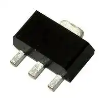
- No. of Pins: 3Pins
- Channel Type: N Channel
- Product Range: -
- Power Dissipation: 28W
- Transistor Mounting: Surface Mount
- Transistor Case Style: SOT-89
- Operating Frequency Max: 941MHz
- Operating Frequency Min: 136MHz
- Drain Source Voltage Vds: 30VDC
- Operating Temperature Max: 150°C
- Continuous Drain Current Id: -
| Delivery and price | |
|---|---|
| Units per pack | 250 |
| Price | 4.65 € |
| Current stock | 500+ |
| Lead time | 30 days |
**Freescale Semiconductor**
Document Number: AFT05MS004N Rev. 0, 7/2014
Technical Data
## **RF Power LDMOS Transistor** High Ruggedness N--Channel Enhancement--Mode Lateral MOSFET
Designed for handheld two--way radio applications with frequencies from 136 to 941 MHz. The high gain, ruggedness and wideband performance of this device make it ideal for large--signal, common--source amplifier applications in handheld radio equipment.
## **Narrowband Performance** (7.5 Vdc, TA = 25C, CW)
|**Frequency**|||**Gps**|**Gps**|||**D**||||**Pout**|
|---|---|---|---|---|---|---|---|---|---|---|---|
|**(MHz)**|||**(dB)**||||**(%)**||||**(W)**|
|520 **(1)**|||20.9||||74.9||||4.9|
|**Wideband Performance** (7.5 Vdc, TA= 25||||= 25C, CW)||||||||
|**Frequency**|**Pin**||||**Gps**|||**D**|||**Pout**|
|**(MHz)**|**(W)**||||**(dB)**||**(%)**||||**(W)**|
|136–174 **(2)**|0.10||||17.8||61.8||||6.1|
|350–520 **(3)**|0.12||||15.4||49.4||||4.2|
|**Load Mismatch/Ruggedness**||||||||||||
|**Frequency**<br>**Signal**|||||**Pin**|||**Test**||||
|**(MHz)**<br>**Type**|**VSWR**||||**(W)**|||**Voltage**|||**Result**|
|435**(3)**<br>CW|> 65:1 at all|> 65:1 at all|||0.24|||9.0|||No Device|
||Phase Angles|||(3 dB Overdrive)|(3 dB Overdrive)||||||Degradation|
## **Wideband Performance** (7.5 Vdc, TA = 25C, CW)
## **Load Mismatch/Ruggedness**
1. Measured in 520 MHz narrowband test circuit.
2. Measured in 136–174 MHz VHF broadband reference circuit.
3. Measured in 350–520 MHz UHF broadband reference circuit.
## **AFT05MS004NT1**
**136–941 MHz, 4 W, 7.5 V WIDEBAND RF POWER LDMOS TRANSISTOR**
**==> picture [31 x 7] intentionally omitted <==**
**----- Start of picture text -----**<br>
SOT--89<br>**----- End of picture text -----**<br>
**==> picture [64 x 79] intentionally omitted <==**
**----- Start of picture text -----**<br>
Source<br>2<br>1 2 3<br>Gate Source Drain<br>**----- End of picture text -----**<br>
## **Features**
- Characterized for Operation from 136 to 941 MHz
**Figure 1. Pin Connections**
- Unmatched Input and Output Allowing Wide Frequency Range Utilization
- Integrated ESD Protection
- Integrated Stability Enhancements
- Wideband — Full Power Across the Band
- Exceptional Thermal Performance
- Extreme Ruggedness
- In Tape and Reel. T1 Suffix = 1,000 Units, 12 mm Tape Width, 7--inch Reel.
## **Typical Applications**
- Output Stage VHF Band Handheld Radio
- Output Stage UHF Band Handheld Radio
- Output Stage for 700–800 MHz Handheld Radio
- Driver for 10–1000 MHz Applications
**AFT05MS004NT1** freescale
Freescale Semiconductor, Inc., 2014. All rights reserved.
**AFT05MS004NT1**
RF Device Data Freescale Semiconductor, Inc.
1
## **Table 1. Maximum Ratings**
|**Table 1. Maximum Ratings**||||||
|---|---|---|---|---|---|
|**Rating**|||**Symbol**|**Value**|**Unit**|
|Drain--Source Voltage|||VDSS|–0.5, +30|Vdc|
|Gate--Source Voltage|||VGS|–6.0, +12|Vdc|
|Operating Voltage|||VDD|12.5, +0|Vdc|
|Storage Temperature Range|||Tstg|–65 to +150|C|
|Case Operating Temperature Range|||TC|–40 to +150|C|
|Operating Junction Temperature Range **(1,2)**|||TJ|–40 to +150|C|
|Total Device Dissipation @ TC= 25C|||PD|28|W|
|Derate above 25C||||0.23|W/C|
|**Table 2. Thermal Characteristics**||||||
|**Characteristic**<br>**Symbol**<br>**Value (2,3)**<br>**Unit**<br>Thermal Resistance, Junction to Case<br>Case Temperature 79C, 4.0 W CW, 7.5 Vdc, IDQ= 100 mA, 520 MHz<br>RJC<br>4.4<br>C/W<br>~~ee~~||||||
|**Table 3. ESD Protection Characteristics**||||||
|**Test Methodology**<br>**Class**<br>Human Body Model (per JESD22--A114)<br>1C, passes 1000 V<br>Machine Model (per EIA/JESD22--A115)<br>A, passes 100 V<br>Charge Device Model (per JESD22--C101)<br>IV, passes 2000 V<br>**Table 4. Moisture Sensitivity Level**<br>**Test Methodology**<br>**Rating**<br>**Package Peak Temperature**<br>**Unit**<br>Per JESD22--A113, IPC/JEDEC J--STD--020<br>1<br>260<br>C<br>~~=~~||||||
|**Table 5. Electrical Characteristics** (TA= 25C unless otherwise noted)||||||
|**Characteristic**||**Symbol**|**Min**|**Typ**<br>**Max**|**Unit**|
|**Off Characteristics**||||||
|Zero Gate Voltage Drain Leakage Current<br>(VDS= 30 Vdc, VGS= 0 Vdc)<br>IDSS<br>—<br>—<br>2<br>Adc<br>Zero Gate Voltage Drain Leakage Current<br>(VDS= 7.5 Vdc, VGS= 0 Vdc)<br>IDSS<br>—<br>—<br>1<br>Adc<br>Gate--Source Leakage Current<br>(VGS= 5 Vdc, VDS= 0 Vdc)<br>IGSS<br>—<br>—<br>500<br>nAdc<br>~~ae~~||||||
|**On Characteristics**||||||
|Gate Threshold Voltage<br>(VDS= 10 Vdc, ID= 67Adc)<br>VGS(th)<br>1.7<br>2.2<br>2.5<br>Vdc<br>Drain--Source On--Voltage<br>(VGS= 10 Vdc, ID= 700 mAdc)<br>VDS(on)<br>—<br>.22<br>—<br>Vdc<br>Forward Transconductance<br>(VDS= 7.5 Vdc, ID= 4.0 Adc)<br>gfs<br>—<br>4.0<br>—<br>S<br>~~Se~~||||||
|**Dynamic Characteristics**||||||
|Reverse Transfer Capacitance<br>(VDS= 7.5 Vdc30 mV(rms)ac @ 1 MHz, VGS= 0 Vdc)<br>Crss<br>—<br>1.63<br>—<br>pF<br>Output Capacitance<br>(VDS= 7.5 Vdc30 mV(rms)ac @ 1 MHz, VGS= 0 Vdc)<br>Coss<br>—<br>34.8<br>—<br>pF<br>Input Capacitance<br>(VDS= 7.5 Vdc, VGS= 0 Vdc30 mV(rms)ac @ 1 MHz)<br>Ciss<br>—<br>57.6<br>—<br>pF<br>~~aan~~||||||
|1. Continuous use at maximum temperature will affect MTTF.||||||
|2. MTTF calculator available athttp://www.freescale.com/rf<br>.Select Software & Tools/Development Tools/Calculators to access MTTF||||Select Software & Tools/Development Tools/Calculators to access MTTF||
|calculators by product.||||||
3. Refer to AN1955, _Thermal Measurement Methodology of RF Power Amplifiers._ Go to http://www.freescale.com/rf. Select Documentation/Application Notes -- AN1955.
(continued)
**AFT05MS004NT1**
RF Device Data Freescale Semiconductor, Inc.
2
**Table 5. Electrical Characteristics** (TA = 25C unless otherwise noted) **(continued)**
**Characteristic Symbol Min Typ Max Unit** ~~a~~ **Functional Tests** (In Freescale Narrowband Test Fixture, 50 ohm system) VDD = 7.5 Vdc, IDQ = 100 mA, Pin = 16 dBm, f = 520 MHz Common--Source Amplifier Output Power Pout — 4.9 — W Drain Efficiency D — 74.9 — % ~~————ee ee ee ee ee~~
**AFT05MS004NT1**
RF Device Data Freescale Semiconductor, Inc.
3
## **TYPICAL CHARACTERISTICS**
**==> picture [238 x 446] intentionally omitted <==**
**----- Start of picture text -----**<br>
100<br>Ciss<br>——<br>OrrCC<br>TE<br>tt Coss<br>Measured with 30 mV(rms)ac @ 1 MHz, VGS = 0 Vdc<br>10<br>[_<br>se<br>a<br>a<br>Crss<br>1 ee a ee ee ee ee<br>0 2 4 6 8 10 12<br>VDS, DRAIN--SOURCE VOLTAGE (VOLTS)<br>Figure 2. Capacitance versus Drain--Source Voltage<br>10 [9]<br>seee<br>VDD = 7.5 Vdc<br>ID = 0.62 Amps<br>————<br>10 [8] r e e ee eee<br>0.77 Amps<br>10 [7]<br>a oo 0.91 Amps<br>Es es<br>a<br>10 [6] aeeee<br>90 100 110 120 130 140 150 160<br>TJ, JUNCTION TEMPERATURE (C)<br>Note: MTTF value represents the total cumulative operating time<br>under indicated test conditions.<br>MTTF calculator available at http://www.freescale.com/rf. Select<br>Software & Tools/Development Tools/Calculators to access MTTF<br>calculators by product.<br>C, CAPACITANCE (pF)<br>MTTF (HOURS)<br>**----- End of picture text -----**<br>
**Figure 2. Capacitance versus Drain--Source Voltage**
**Figure 3. MTTF versus Junction Temperature — CW**
**AFT05MS004NT1**
RF Device Data Freescale Semiconductor, Inc.
4
## **520 MHz NARROWBAND PRODUCTION TEST FIXTURE**
**==> picture [473 x 533] intentionally omitted <==**
**----- Start of picture text -----**<br>
|||||||||||||||||||||
|---|---|---|---|---|---|---|---|---|---|---|---|---|---|---|---|---|---|---|---|
|V|—|GG|C3|B1|C11|\|VDD|
|eo00000000°|potc|ILI|o00000000000000000|°°|°°|lo000000000000|Fete||||[|7O|pooo0000|
|°|C2|o|||°|°|°|C10|°|
|°°|8°|C1|C4|9[||8°°|8°°|[|°|C9|C12|\|°°3|
|°|o]|°|°|°|°|
|°|||°|°|°|°|
|°|
|°|°||°|°°|QO|O|O|°°|°°|°°|
|°|
|$|°|©|®|8|r|°|0000000000|4,|coovccccc000|°|“Ip|.|8|)|®|°$|
|oO°|09200000000000|C7|oo|°|R6|ft|ol|R1|esese|=F|—|—|L1|loao|0000009|C13|02900000|fo°|
|R2|
|C16|
|C5|R3|L2|
|R4|
|°oo°|©|6806000000000|H(J|R5|coobass||{oe|o0o0TT|e|TOOOOSe|C8|°°|
|°°°|°°|°|C6|‘|°|000.000000000000O|OlodBs°°|0000000000O|0|C15||_|m|-—000||e_|oe|C14|°°|°|°°|
|AFT05MS004N|
|s-*|f|reescale”|D57923|Rev. 0|
|semiconductor|
|°|
|°|°|
|°|°|
|°|°|
|0000000000000000000000000000000000|000000|000000|0000000000000000000000000000000000|
|Figure 4. AFT05MS004NT1 Narrowband Test Circuit Component Layout — 520 MHz|
|Table 6. AFT05MS004NT1 Narrowband Test Circuit Component Designations and Values — 520 MHzponent Designations and Values — 520 MHzonent Designations and Values — 520 MHzgnations and Values — 520 MHznations and Values — 520 MHz|
|Part|Description|Part Number|Manufacturer|
|B1|RF Bead, Short|2743019447|Fair--Rite|
|C1|22 F, 35 V Tantalum Capacitor|T491X226K035AT|Kemet|
|C2, C11|0.1 F Chip Capacitors|CDR33BX104AKWS|AVX|
|C3, C10|0.01 F Chip Capacitors|C0805C103K5RAC|Kemet|
|C4, C9|180 pF Chip Capacitors|ATC100B181JT300XT|ATC|
|C5|11 pF Chip Capacitor|ATC100B110JT500XT|ATC|
|C6, C7|13 pF Chip Capacitors|ATC100B130JT500XT|ATC|
|C8, C15|2.2 pF Chip Capacitors|ATC100B2R2JT500XT|ATC|
|C12|330 F, 35 V Electrolytic Capacitor|MCGPR35V337M10X16--RH|Multicomp|
|C13, C14|16 pF Chip Capacitors|ATC100B160JT500XT|ATC|
|C16|9.1 pF Chip Capacitor|ATC100B9R1CT500XT|ATC|
|L1|8.0 nH, 3 Turn Inductor|A03TKLC|Coilcraft|
|L2|5 nH, 2 Turn Inductor|A02TKLC|Coilcraft|
|R1, R2, R3, R4, R5|1.5 , 1/4 W Chip Resistors|RC1206FR--071R5L|Yageo|
|R6|27 , 1/4 W Chip Resistor|CRCW120627R0FKEA|Vishay|
|PCB|Rogers RO4350, 0.030, r|= 3.66|D57923|MTL|
**----- End of picture text -----**<br>
**Table 6. AFT05MS004NT1 Narrowband Test Circuit Component Designations and Values — 520 MHzponent Designations and Values — 520 MHzonent Designations and Values — 520 MHzgnations and Values — 520 MHznations and Values — 520 MHz**
**AFT05MS004NT1**
RF Device Data Freescale Semiconductor, Inc.
5
**==> picture [392 x 599] intentionally omitted <==**
**----- Start of picture text -----**<br>
r<br>;<br><. ll<br>RF<br>OUTPUT<br>Z16<br>C16<br>Z15<br>C8<br>SUPPLY Z14<br>V<br>L2<br>+ C12<br>Taper Microstrip<br><br>Z13<br>C11 3 C14 Description Microstrip Microstrip 0.320 Microstrip Microstrip Microstrip Microstrip Microstrip<br>C1 <br>Z12<br>C10<br>0.620 0.620 0.620 0.320 0.320 0.120 0.120 0.080<br>Z11<br> <br>C9<br>Z10<br>L1 C15 0.708 0.062 0.162 0.377 0.055 0.587 0.078 0.238<br>Z9<br>Microstrip Z9 Z10 Z11 Z12 Z13 Z14 Z15 Z16<br>DUT<br>Z8<br>R1 R2 R3 R4 R5<br>Z7 Taper Microstrip<br><br>0.620<br>R6 Description Microstrip Microstrip Microstrip Microstrip Microstrip Microstrip Microstrip<br>Z6 <br>C4 Z5 0.080 0.120 0.320 0.320 0.320 0.620 0.620 0.620<br> <br>Figure 5. AFT05MS004NT1 Narrowband Test Circuit Schematic — 520 MHz<br>Z4<br>B1 C6 0.328 0.490 0.055 0.555 0.160 0.045 0.387 0.273<br>C7<br>Z3<br>C3<br>C5 Microstrip Z1 Z2 Z3 Z4 Z5 Z6 Z7 Z8<br>Table 7. AFT05MS004NT1 Narrowband Test Circuit Microstrips — 520 MHz<br>C2<br>Z2<br>+ C1<br>Z1<br>BIAS RF<br>V INPUT<br>**----- End of picture text -----**<br>
**AFT05MS004NT1**
RF Device Data Freescale Semiconductor, Inc.
6
**TYPICAL CHARACTERISTICS — 520 MHz NARROWBAND REFERENCE CIRCUIT**
**==> picture [273 x 624] intentionally omitted <==**
**----- Start of picture text -----**<br>
6<br>VDD = 7.5 Vdc, f = 520 MHz<br>Po<br>5<br>4<br>Pin = 0.04 W<br>3 ee ae<br>2 Ptf fAZ]<br>Pin = 0.02 W<br>Pf<br>1<br>0 | |wrLs YZ<br>1 1.5 2 2.5 3 3.5<br>VGS, GATE--SOURCE VOLTAGE (VOLTS)<br>Figure 6. Output Power versus Gate--Source Voltage<br>2421 Te 9080<br>Gps<br>18 a. 70<br>15 ey ae 60<br>12 FT EEE 50<br>9 > eeee 40<br>D<br>6 30<br>3 Pout VDD = 7.5 Vdc, IDQ = 100 mA 20<br>f = 520 MHz<br>0 A 10<br>0 0.02 0.04 0.06 0.08 0.1<br>Pin, INPUT POWER (WATTS)<br>Figure 7. Power Gain, Drain Efficiency and Output<br>Power versus Input Power<br>VDD = 7.5 Vdc, IDQ = 100 mA, Pout = 4 W<br>f Zsource Zload<br>MHz <br>520 1.35 + j2.15 2.10 + j1.70<br>Zsource = Test circuit impedance as measured from<br>gate to ground.<br>Zload = Test circuit impedance as measured from<br>drain to ground.<br>Input Device Output<br>Matching Under Matching<br>Network Test Network<br>50 50 <br>_L e o b<br>Zsource Zload<br>, OUTPUT POWER (WATTS)<br>out<br>P<br>, POWER GAIN (dB)<br>ps<br>G<br>, OUTPUT POWER (WATTS) , DRAIN EFFICIENCY (%)<br>out D<br>P<br>**----- End of picture text -----**<br>
**Figure 8. Narrowband Series Equivalent Source and Load Impedance — 520 MHz**
**AFT05MS004NT1**
RF Device Data Freescale Semiconductor, Inc.
7
## **136–174 MHz VHF BROADBAND REFERENCE CIRCUIT**
|**Table 8. 136–174 MHz VHF Broadband Performance** (In Freescale Reference Circuit, 50 ohm system)|**Table 8. 136–174 MHz VHF Broadband Performance** (In Freescale Reference Circuit, 50 ohm system)|**Table 8. 136–174 MHz VHF Broadband Performance** (In Freescale Reference Circuit, 50 ohm system)|**Table 8. 136–174 MHz VHF Broadband Performance** (In Freescale Reference Circuit, 50 ohm system)|
|---|---|---|---|
|VDD= 7.5 Volts, IDQ= 100 mA, TA= 25C, CW||||
|**Frequency**<br>**(MHz)**<br>**Pin**<br>**(W)**<br>**Gps**<br>**(dB)**<br>**D**<br>**(%)**<br>**Pout**<br>**(W)**<br>135<br>0.10<br>17.8<br>62.3<br>6.0<br>155<br>0.06<br>20.2<br>69.1<br>6.0<br>175<br>0.10<br>17.9<br>61.8<br>6.0<br>~~——————~~||||
|**Table 9. Load Mismatch/Ruggedness**(In Freescale Reference Circuit)||||
|**Frequency**<br>**Signal**|**Pin**|||
|**(MHz)**<br>**Type**|**VSWR**<br>**(W)**<br>**Test Voltage, VDD**||**Result**|
|155<br>CW|> 65:1 at all<br>0.2<br>9.0||No Device|
||Phase Angles<br>(3 dB Overdrive)||Degradation|
**AFT05MS004NT1**
RF Device Data Freescale Semiconductor, Inc.
8
## **136–174 MHz VHF BROADBAND REFERENCE CIRCUIT**
**==> picture [393 x 209] intentionally omitted <==**
**----- Start of picture text -----**<br>
J1<br>C11 C12<br>aie) | C1 fe)e) Q (a[e[e| » fe)O | re)<br>O| Fo fe) fe) | e) C10<br>0) e)|e LOX C13 C14 C15 | | | L4 + C16 @)= C17 C18 O| E e C9<br>o© OoO° eeini| 5 5) E+] eeTt ofoL ofL_th TL Oo[2 L6<br>C2 of I] o eo 2909 |_| fo o| [—WI]O] = [0][0][0][0] OC} IS<br>— ie) o<S¢ ry fete. _— fe) O <T 6 C8<br>C3<br>R1 Q1<br>L1<br>F A 00 P0000 i—h 00000] E t °<br>C4 L3 L5<br>L2<br>att |] ¢§———_ — | ae ©<br>C7<br>CAA : :<br>CST C5 C6 ypoes O <eec yeeee<br>5 0fe) °Ob S555 5506?<br>D61839 000000 AFT05MS004N Rev. 0 (136 – 174 MHz)<br>**----- End of picture text -----**<br>
**Figure 9. AFT05MS004NT1 VHF Broadband Reference Circuit Component Layout — 136–174 MHz**
**Table 10. AFT05MS004NT1 VHF Broadband Reference Circuit Component Designations and Values — 136–174 MHz**
|**Part**|**Description**|**Part Number**|**Manufacturer**|
|---|---|---|---|
|C1, C10, C14, C17|1 nF Chip Capacitors|2012X7R2E102M|TDK|
|C2|39 pF Chip Capacitor|ATC600F390JT250XT|ATC|
|C3, C8|56 pF Chip Capacitors|ATC600F560JT250XT|ATC|
|C4, C5|68 pF Chip Capacitors|ATC600F680JT250XT|ATC|
|C6, C15, C16|100 pF Chip Capacitors|ATC600F101JT250XT|ATC|
|C7|150 pF Chip Capacitor|ATC600F151JT250XT|ATC|
|C9|8.2 pF Chip Capacitor|ATC600F8R2BT250XT|ATC|
|C11, C12|10F, 50 V Electrolytic Capacitors|UVR1H100MDD|Nichicon|
|C13, C18|1F Chip Capacitors|GRM21BR71H105KA12L|Murata|
|J1|Breakaway Header, Right--Angle 3 Pins|22-28-8360|Molex|
|L1|13.7 nH Inductor|0807SQ14N|Coilcraft|
|L2|12.3 nH Inductor|0806SQ12N|Coilcraft|
|L3, L4|25.0 nH Inductors|0908SQ25N|Coilcraft|
|L5|15.7 nH Inductor|0806SQ16N|Coilcraft|
|L6|27.3 nH Inductor|0908SQ27N|Coilcraft|
|Q1|RF Power LDMOS Transistor|AFT05MS004NT1|Freescale|
|R1|33, 1/10 W Chip Resistor|CRCW080533R0JNEA|Vishay|
|PCB|0.020,r = 4.8, FR4(S--1000)|D61839|MTL|
**AFT05MS004NT1**
RF Device Data Freescale Semiconductor, Inc.
9
**==> picture [418 x 642] intentionally omitted <==**
**----- Start of picture text -----**<br>
;<br>-<br>RF<br>OUTPUT<br>Z22<br>C10<br>Z21<br>C9<br>Z20<br>Microstrip Microstrip Microstrip Microstrip Microstrip Microstrip Microstrip<br> <br>SUPPLY L6 0.170 0.050 0.050 0.050 0.050 0.050 0.050<br>V Z19 Description <br>+ C12 C8<br>0.015 0.357 0.010 0.010 0.010 0.010 0.120<br>Z18<br>C18<br>C17 L5<br>C16 Z17 C7 Microstrip Z16 Z17* Z18 Z19 Z20 Z21 Z22<br>Z15 L4 Z14 L3 Z16<br>Z13 Microstrip Microstrip Microstrip Microstrip Microstrip Microstrip Microstrip<br>Z12 DUT 0.300 0.300 0.140 0.140 0.170 0.084 0.040<br>Description<br> <br>0.070 0.032 0.070 0.070 0.015 0.030 0.040<br>Z11<br>R1 Z10<br>C15 Z9 Microstrip Z9 Z10 Z11 Z12 Z13 Z14 Z15<br>C14 L2<br>C13 Z8 C6<br>Microstrip Microstrip Microstrip Microstrip Microstrip Microstrip Microstrip Microstrip<br>+ C11 Z7 <br>C5 0.050 0.050 0.050 0.050 0.050 0.050 0.040 0.040<br>Description<br>Z6 <br>BIAS C4<br>V<br>Z5 0.120 0.142 0.010 0.012 0.010 0.010 0.012 0.265<br>L1 Figure 10. AFT05MS004NT1 VHF Broadband Reference Circuit Schematic — 136–174 MHz<br>Z4 C3 Table 11. AFT05MS004NT1 VHF Broadband Reference Circuit Microstrips — 136–174 MHz Microstrip Z1 Z2 Z3 Z4 Z5 Z6* Z7 Z8 * Line length includes microstrip bends<br>Z3<br>C2<br>Z2<br>C1<br>Z1<br>RF<br>INPUT<br>**----- End of picture text -----**<br>
**AFT05MS004NT1**
RF Device Data Freescale Semiconductor, Inc.
10
**TYPICAL CHARACTERISTICS — 136–174 MHz VHF BROADBAND REFERENCE CIRCUIT**
**==> picture [276 x 174] intentionally omitted <==**
**----- Start of picture text -----**<br>
22 90<br>21 80<br>20 eeee D 70<br>19 60<br>Serr<br>18 eeSs 50<br>Gps<br>17 Po ee ee ee 8<br>16 | | |tThvE h| | | 7<br>15 LT V P DD in = 0.1 W = 7.5 Vdc PP Pout 6<br>14 | | I DQ = 100 mA | | 5<br>13 4<br>| | [ot]<br>135 140 145 150 155 160 165 170 175<br>f, FREQUENCY (MHz)<br>, DRAIN<br>D<br><br>EFFICIENCY (%)<br>, POWER GAIN (dB)<br>ps<br>G<br>, OUTPUT<br>out<br>P<br>POWER (WATTS)<br>**----- End of picture text -----**<br>
**Figure 11. Power Gain, Drain Efficiency and Output Power versus Frequency at a Constant Pin**
**==> picture [454 x 174] intentionally omitted <==**
**----- Start of picture text -----**<br>
6<br>f = 155 MHz<br>1<br>f = 155 MHz<br>5<br>0.8<br>4 ee VDD = 7.5 Vdc, Pin = 0.1 W ee VDD = 7.5 Vdc<br>0.6 Pin = 0.1 W<br>3 pi [i<br>| VDD = 7.5 Vdc, P | in = 0.05 W ts 0.4 VDD = 7.5 Vdc IT<br>2 Pin = 0.05 W<br>ee sae 0.2 LI<br>1<br>Detail A 0<br>0 0.5 1 1.5 2 2.5<br>0 pttepA_ —| lt | I —| pT 4<br>0 0.5 1 1.5 2 2.5 3 3.5 VGS, GATE--SOURCE VOLTAGE (VOLTS)<br>VGS, GATE--SOURCE VOLTAGE (VOLTS) Detail A<br>, OUTPUT POWER (WATTS) , OUTPUT POWER (WATTS)<br>Pout Pout<br>**----- End of picture text -----**<br>
**Figure 12. Output Power versus Gate--Source Voltage**
**==> picture [278 x 174] intentionally omitted <==**
**----- Start of picture text -----**<br>
25 80<br>24 VDD = 7.5 Vdc 155 MHz D 70<br>23 I DQ = 100 mA 60<br>22 175 MHz 50<br>21 ee a= a 135 MHz 40<br>20 ss 2.4 | 30<br>19 155 MHz 20<br>18 peSS [| [|] 10 3<br>17 175 MHz P out 8<br>16 oe 135 MHz LTRS AL 7<br>15 ——| |Hi|_| pS Gps 6<br>14 155 MHz 5<br>13 175 MHz 4<br>12 pT Nea| 3<br>11 135 MHz 2<br>10 Eert ee 1<br>9 eeHf [OOO] fe HEE ee 0 3<br>0.01 0.1 0.3<br>Pin, INPUT POWER (WATTS)<br>, DRAIN<br>D<br><br>EFFICIENCY (%)<br>, POWER GAIN (dB)<br>ps<br>G<br>, OUTPUT<br>out<br>P<br>POWER (WATTS)<br>**----- End of picture text -----**<br>
**Figure 13. Power Gain, Drain Efficiency and Output Power versus Input Power and Frequency**
**AFT05MS004NT1**
RF Device Data Freescale Semiconductor, Inc.
11
## **136–174 MHz VHF BROADBAND REFERENCE CIRCUIT**
**==> picture [442 x 212] intentionally omitted <==**
**----- Start of picture text -----**<br>
f = 175 MHz Zo = 25 <br>KPof fe Komi»BOSS55Xx) f = 135 MHz 00sSAS<S A SSE e —— SIT Le <on%<br>QERLLERK SSS TS<br>BLEED x T CT RSS<br>/ LYS Se SXO rer TAOS<br>TE REEL Zsource TON, Mectetetienc gtvebeetet Gmmns nas:<br>ISLPAIfe Ie EERERELL BEIEERE PSSLR SkeSLLLLLmuses<br>eT]Teh bdHOLT RRS oS eH<br>Sf /8f ABPELE OAR SIE<br>2 yi te maaetan eae ee<br>ef hk FPET ERT DR<br>gf [of Hyi: Ree eereliewmeeletnseer<br>afte 8 os Zload eeeee ereeteeoeanninc cam of<br>g PtHeigaHEEeiiuaie Perreeststtuueerstiiceeaia:<br>W e eee eerererereeemsiris geese) ate<br>f = 175 MHz S| 1st Pata tariel EEEEEETEE CLP Oy<br>f = 135 MHz<br>**----- End of picture text -----**<br>
VDD = 7.5 Vdc, IDQ = 100 mA, Pout = 4 W
||||||**f**||||**Zsource**||**Zload**|||||
|---|---|---|---|---|---|---|---|---|---|---|---|---|---|---|---|
||||||**MHz**|||||||||||
||||||135||||7.02 + j13.05|2.24 - j1.21||||||
||||||140||||8.07 + j13.00|2.42 - j0.87||||||
||||||145||||9.05 + j12.43|2.56 - j0.54||||||
||||||150||||9.68 + j11.26|2.79 - j0.24||||||
||||||155||||9.16 + j9.82|3.08 - j0.07||||||
||||||160||||7.39 + j9.21|3.23 - j0.03||||||
||||||165||||5.83 + j10.15|3.52 - j0.09||||||
||||||170||||5.09 + j11.62|3.77 - j0.01||||||
||||||175||||5.06 + j12.97|3.40 - j0.27||||||
|||||Zsource||=|Test circuit impedance as measured from|||||||||
||||||||gate to ground.|||||||||
|||||Zload||=|Test circuit impedance as measured from|||||||||
||||||||drain to ground.|||||||||
|||||Input|||||Device||Output|||||
|50||||Matching<br>Network|||||Under<br>Test||Matching<br>Network||||50|
|||||||||||||||||
|||||||||||||||||
||||||||||**Zsource**<br>**Zload**|||||||
**Figure 14. VHF Broadband Series Equivalent Source and Load Impedance — 136–174 MHz**
**AFT05MS004NT1**
RF Device Data Freescale Semiconductor, Inc.
12
## **350–520 MHz UHF BROADBAND REFERENCE CIRCUIT**
|**Table 12. 350–520 MHz UHF Broadband Performance** (In Freescale Reference Circuit, 50 ohm system)|**Table 12. 350–520 MHz UHF Broadband Performance** (In Freescale Reference Circuit, 50 ohm system)|**Table 12. 350–520 MHz UHF Broadband Performance** (In Freescale Reference Circuit, 50 ohm system)|**Table 12. 350–520 MHz UHF Broadband Performance** (In Freescale Reference Circuit, 50 ohm system)|**Table 12. 350–520 MHz UHF Broadband Performance** (In Freescale Reference Circuit, 50 ohm system)|(In Freescale Reference Circuit, 50 ohm system)|
|---|---|---|---|---|---|
|VDD= 7.5 Volts, IDQ= 50 mA, TA= 25C, CW||||||
|**Frequency**<br>**(MHz)**<br>**Pin**<br>**(W)**<br>**Gps**<br>**(dB)**<br>**D**<br>**(%)**<br>**Pout**<br>**(W)**<br>350<br>0.11<br>15.5<br>48.7<br>4.0<br>470<br>0.04<br>19.8<br>67.7<br>4.0<br>520<br>0.09<br>16.3<br>71.1<br>4.0<br>~~——————~~||||||
|**Table 13. Load Mismatch/Ruggedness**(In Freescale Reference Circuit)||||||
|**Frequency**<br>**Signal**|**Pin**|||||
|**(MHz)**<br>**Type**<br>**VSWR**|**(W)**||**Test Voltage, VDD**||**Result**|
|435<br>CW<br>> 65:1 at all|0.24||9.0||No Device|
|Phase Angles|(3 dB Overdrive)||||Degradation|
**AFT05MS004NT1**
RF Device Data Freescale Semiconductor, Inc.
13
## **350–520 MHz UHF BROADBAND REFERENCE CIRCUIT**
**==> picture [377 x 206] intentionally omitted <==**
**----- Start of picture text -----**<br>
J1<br>B1 B2<br>O C6 C7 O<br>C1 |° FA foo| | L COo000td Ly | IE IS 00000 | o|Jo Fy° C12<br>L1 ie)roO] e | | fo)|eO C5 a n R1 © of Oo eS — C8 |q hL L5 FO C11<br>° Fj Jo | © OC} E4 || of ] |°<br>L3<br>fo) pl o5 C2 cogooa tdo o ] 5 8 [hh foO otSlooo00 6q ni ° C10<br>Q1<br>R2<br>L4<br>L2 ° F It R|oodoo000oe — 7 a opsod t °<br>5 I |° PSA O oO 0 CO)o| gF Y 5<br>C4 C9<br>5 e a e WU p ea l 5<br>C3<br>fe) | 6 fe)<br>os o jooes° © °°°0556000000Foc yoooo®<br>o fe)<br>D56664 O00000 AFT05MS004N Rev. 0 (350 – 520 MHz)<br>**----- End of picture text -----**<br>
**Figure 15. AFT05MS004NT1 UHF Broadband Reference Circuit Component Layout — 350–520 MHz**
**Table 14. AFT05MS004NT1 UHF Broadband Reference Circuit Component Designations and Values — 350–520 MHz**
|**Part**|**Description**|**Part Number**|**Manufacturer**|
|---|---|---|---|
|B1, B2|RF Beads|2743019447|Fair--Rite|
|C1, C10|18 pF Chip Capacitors|GQM2195C2E180FB12D|Murata|
|C5, C8, C12|100 pF Chip Capacitors|GQM2195C2E101GB12D|Murata|
|C2, C3|15 pF Chip Capacitors|GQM2195C2E150FB12D|Murata|
|C4|56 pF Chip Capacitor|GQM2195C2E560GB12D|Murata|
|C6|1F Chip Capacitor|GRM31CR72A105KA01L|Murata|
|C7|10F Chip Capacitor|GRM31CR61H106KA12L|Murata|
|C9|39 pF Chip Capacitor|GQM2195C2E390GB12D|Murata|
|C11|5.1 pF Chip Capacitor|GQM2195C2E5R1BB12D|Murata|
|J1|Breakaway Header, Right--Angle 3 Pins|22-28-8360|Molex|
|L1, L2|5.5 nH Inductors|0806SQ5N5|Coilcraft|
|L3|16.6 nH Inductor|0908SQ17N|Coilcraft|
|L4|2.55 nH Inductor|0906--3JLC|Coilcraft|
|L5|8.1 nH Inductor|0908SQ8N1|Coilcraft|
|Q1|RF Power LDMOS Transistor|AFT05MS004NT1|Freescale|
|R1, R2|22, 1/10 W Chip Resistors|RR1220Q--220--D|Susumu|
|PCB|0.020,r = 4.8, FR4(S--1000)|D56664|MTL|
**AFT05MS004NT1**
RF Device Data Freescale Semiconductor, Inc.
14
**==> picture [350 x 637] intentionally omitted <==**
**----- Start of picture text -----**<br>
_<br>RF<br>OUTPUT<br>Z24<br>C12<br>Z23<br>C11<br>Z22 Microstrip Microstrip Microstrip Microstrip Microstrip Microstrip Microstrip Microstrip<br> <br>L5<br>0.170 0.050 0.050 0.050 0.050 0.050 0.050 0.050<br>Description<br>SUPPLY <br>V Z21 C10 0.190 0.150 0.270 0.070 0.070 0.050 0.050 0.150<br>C7 Z20<br>B2 L4<br>C8 Microstrip Z17 Z18 Z19* Z20 Z21 Z22 Z23 Z24<br>Z19 C9<br>Z16 Z18<br>L3 Z15 Z17<br>Microstrip Microstrip Microstrip Microstrip Microstrip Microstrip Microstrip Microstrip<br> <br>Z14 0.060 0.034 0.300 0.140 0.140 0.170 0.060 0.034<br>Description<br> <br>Z13<br>0.140 0.065 0.057 0.070 0.070 0.057 0.140 0.200<br>DUT<br>Z12<br>Microstrip Z9 Z10 Z11 Z12 Z13 Z14 Z15 Z16<br>R1 Z9 R2 Z11<br>Z8<br>Z10<br>Z7<br>C5<br>C4 Microstrip Microstrip Microstrip Microstrip Microstrip Microstrip Microstrip Microstrip<br> <br>B1 Z6 0.050 0.050 0.050 0.050 0.050 0.050 0.300<br>C3 Description x 0.050<br>C6 <br>Z5 0.150 0.090 0.070 0.070 0.090 0.160 0.260 0.095<br>BIAS L2<br>V<br>Z4 Figure 16. AFT05MS004NT1 UHF Broadband Reference Circuit Schematic — 350–520 MHz<br>C2<br>Table 15. AFT05MS004NT1 UHF Broadband Reference Circuit Microstrips — 350–520 MHz Microstrip Z1 Z2 Z3 Z4 Z5* Z6* Z7 Z8 * Line length includes microstrip bends<br>Z3<br>L1<br>Z2<br>C1<br>Z1<br>RF<br>INPUT<br>**----- End of picture text -----**<br>
**AFT05MS004NT1**
RF Device Data Freescale Semiconductor, Inc.
15
## **TYPICAL CHARACTERISTICS — 350–520 MHz UHF BROADBAND REFERENCE CIRCUIT**
**==> picture [276 x 174] intentionally omitted <==**
**----- Start of picture text -----**<br>
20 80<br>D<br>19 70<br>pf | |be<br>18 P| tae] | tt tt 60<br>17 50<br>pip |<br>16 40<br>| ta | | |Prt Gps<br>15 pet tt 7<br>1413 Ppmma| |Peet| 65<br>12 V P DD in = 0.12 W = 7.5 Vdc Pout 4<br>| + | | Sa| |<br>IDQ = 50 mA<br>11 | tt | tt|N 3<br>340 360 380 400 420 440 460 480 500 520 540<br>f, FREQUENCY (MHz)<br>, DRAIN<br>D<br><br>EFFICIENCY (%)<br>, POWER GAIN (dB)<br>ps<br>G<br>, OUTPUT<br>out<br>P<br>POWER (WATTS)<br>**----- End of picture text -----**<br>
**Figure 17. Power Gain, Drain Efficiency and Output Power versus Frequency at a Constant at a Constant Pin**
**==> picture [451 x 384] intentionally omitted <==**
**----- Start of picture text -----**<br>
6<br>f = 435 MHz<br>1.0<br>f = 435 MHz<br>5<br>0.8<br>4 V DD = 7.5 Vdc, P in = 0.12 W 0.6 VPDDin = = 7.5 Vdc 0.06 W<br>3 V DD = 7.5 Vdc, P in = 0.06 W y| f\ VDD = 7.5 Vdc<br>0.4 Pin = 0.12 W<br>2 WANA<br>PSO 0.2<br>1 £|<br>0<br>Detail A<br>0 0.5 1 1.5 2<br>eeea4<br>0<br>0 0.5 1 1.5 2 2.5 3 VGS, GATE--SOURCE VOLTAGE (VOLTS)<br>VGS, GATE--SOURCE VOLTAGE (VOLTS) Detail A<br>Figure 18. Output Power versus Gate--Source Voltage<br>25 80<br>24 VDD = 7.5 Vdc 435 MHz D 70<br>23 IDQ = 50 mA 350 MHz 60<br>22 520 MHz 50<br>21 a eeroofeeibs 40<br>20 att 435 MHz ee 30<br>19 ws Eee | 20<br>18 eeeee 10<br>17 520 MHz EAL EP 7<br>16 po ee P out 6<br>15 350 MHz 435 MHz SSS 5<br>14 Gps 4<br>1213 a— AT | | | ge 350 MHz S||| 32<br>520 MHz<br>11 | Cr | 1<br>10 ee ee ee eeee| 0<br>0.01 0.1 0.3<br>Pin, INPUT POWER (WATTS)<br>, OUTPUT POWER (WATTS) , OUTPUT POWER (WATTS)<br>Pout Pout<br>, DRAIN<br>D<br><br>EFFICIENCY (%)<br>, POWER GAIN (dB)<br>ps<br>G<br>, OUTPUT<br>out<br>P<br>POWER (WATTS)<br>**----- End of picture text -----**<br>
**Figure 19. Power Gain, Drain Efficiency and Output Power versus Input Power and Frequency**
**AFT05MS004NT1**
RF Device Data Freescale Semiconductor, Inc.
16
## **350–520 MHz UHF BROADBAND REFERENCE CIRCUIT**
**==> picture [384 x 205] intentionally omitted <==**
**----- Start of picture text -----**<br>
(So 8 4 a <x (\F XT 4 | PT<br>f = 520 MHz<br>YUP Sn xo EEE<br>BR EE MSCSSAA<br>he FL OLE Zsource ELON OOO ITI Zo = 5 OE<br>BIL LAO LEER ERM RK REO ORC SS A<br>ef,|8 el PEE TT RI ILO LLLP P SSE<br>| Hse TE f = 350 MHz PLAIDE LOR LSS<br>f = 520 MHz<br>Wie tears me MN ee Oosees ae<br>ee]af[‘] PRaceeeestesee EERE TT IRE D L<br>| HEareee Zload<br>Mls er ee eh<br>“| Greeti et seeec ones cite persPevmeerstsrt ease!<br>EEECEEEEEEEE Resisrauce, cousonent (#5), of conpucrance couibarat(f) ans an<br>f = 350 MHz<br>stil] FEEPeco eee Oe ee CEDs<br>**----- End of picture text -----**<br>
VDD = 7.5 Vdc, IDQ = 50 mA, Pout = 4 W
**==> picture [273 x 399] intentionally omitted <==**
**----- Start of picture text -----**<br>
f Zsource Zload<br>MHz <br>350 2.27 - j1.72 3.55 + j1.20<br>eeee<br>360 2.41 - j1.91 3.61 + j0.92<br>ee ee<br>370 2.55 - j2.11 3.66 + j0.64<br>eeee<br>380 2.68 - j2.31 3.71 + j0.36<br>es ee ee<br>390 2.74 - j2.38 3.71 + j0.15<br>eeee<br>400 2.76 - j2.36 3.69 + j0.02<br>ee ee ee<br>410 ee 2.77 - j2.35 3.66 + j0.18<br>ee ee ee<br>420 2.78 - j2.35 3.67 + j0.34<br>ee ee<br>430 2.78 - j2.43 3.82 + j0.48<br>ee ee<br>440 2.79 - j2.50 3.97 + j0.62<br>ee ee<br>450 2.79 - j2.57 4.13 + j0.76<br>ee ee<br>460 ee 2.44 - j2.70 4.00 + j0.95<br>ee ee<br>470 2.02 - j2.84 3.80 + j1.15<br>ee ee<br>480 1.59 - j2.98 3.61 + j1.36<br>eeee<br>490 1.37 - j3.20 3.53 + j1.46<br>es ee ee<br>500 1.45 - j3.53 3.62 + j1.41<br>ee ee<br>510 ee 1.52 - j3.86 3.71 + j1.36<br>ee ee<br>520 1.60 - j4.19 3.80 + j1.31<br>ee ee ee<br>Zsource = Test circuit impedance as measured from<br>gate to ground.<br>Zload = Test circuit impedance as measured from<br>drain to ground.<br>Input Device Output<br>Matching Under Matching<br>Network Test Network<br>50 50 <br>Zsource Zload<br>**----- End of picture text -----**<br>
**Figure 20. UHF Broadband Series Equivalent Source and Load Impedance — 350–520 MHz**
**AFT05MS004NT1**
RF Device Data Freescale Semiconductor, Inc.
17
**==> picture [255 x 428] intentionally omitted <==**
**----- Start of picture text -----**<br>
1.90<br>3.00<br>2X 4.35<br>45<br>2X<br>1.25<br>3X<br>0.70<br>0.85<br>2X<br>yf 1.50<br>Figure 21. PCB Pad Layout for SOT--89A<br>AFT504<br>AWLYWZ<br>—<br>**----- End of picture text -----**<br>
**Figure 22. Product Marking**
**AFT05MS004NT1**
RF Device Data Freescale Semiconductor, Inc.
18
## **PACKAGE DIMENSIONS**
**AFT05MS004NT1**
RF Device Data Freescale Semiconductor, Inc.
19
**AFT05MS004NT1**
RF Device Data Freescale Semiconductor, Inc.
20
**AFT05MS004NT1**
RF Device Data Freescale Semiconductor, Inc.
21
## **PRODUCT DOCUMENTATION, SOFTWARE AND TOOLS**
Refer to the following documents, software and tools to aid your design process.
## **Application Notes**
- AN1955: Thermal Measurement Methodology of RF Power Amplifiers
## **Engineering Bulletins**
- EB212: Using Data Sheet Impedances for RF LDMOS Devices
## **Software**
- Electromigration MTTF Calculator
- RF High Power Model
- .s2p File
## **Development Tools**
- Printed Circuit Boards
For Software and Tools, do a Part Number search at http://www.freescale.com, and select the “Part Number” link. Go to the Software & Tools tab on the part’s Product Summary page to download the respective tool.
## **REVISION HISTORY**
The following table summarizes revisions to this document. **Revision Date Description** 0 July 2014 Initial Release of Data Sheet ~~pp~~
**AFT05MS004NT1**
RF Device Data Freescale Semiconductor, Inc.
22
## _**How to Reach Us:**_
**Home Page:** freescale.com
**Web Support:** freescale.com/support
Information in this document is provided solely to enable system and software implementers to use Freescale products. There are no express or implied copyright licenses granted hereunder to design or fabricate any integrated circuits based on the information in this document.
Freescale reserves the right to make changes without further notice to any products herein. Freescale makes no warranty, representation, or guarantee regarding the suitability of its products for any particular purpose, nor does Freescale assume any liability arising out of the application or use of any product or circuit, and specifically disclaims any and all liability, including without limitation consequential or incidental damages. “Typical” parameters that may be provided in Freescale data sheets and/or specifications can and do vary in different applications, and actual performance may vary over time. All operating parameters, including “typicals,” must be validated for each customer application by customer’s technical experts. Freescale does not convey any license under its patent rights nor the rights of others. Freescale sells products pursuant to standard terms and conditions of sale, which can be found at the following address: freescale.com/SalesTermsandConditions.
Freescale and the Freescale logo are trademarks of Freescale Semiconductor, Inc., Reg. U.S. Pat. & Tm. Off. Airfast is a trademark of Freescale Semiconductor, Inc. All other product or service names are the property of their respective owners. E 2014 Freescale Semiconductor, Inc.
**AFT05MS004NT1** & freescale
RF Device DataDocument Number: AFT05MS004N Freescale Semiconductor, Inc.Rev. 0, 7/2014
23
Updated at April 10, 2026
NXP Semiconductors is a global leader in secure connectivity solutions, driving innovation across the automotive, industrial, IoT, mobile, and communications infrastructure markets. By developing advanced, purpose-built technologies, NXP enables devices to sense, think, connect, and act intelligently, delivering rigorously tested components that make the connected world safer and more efficient. Within the semiconductor space, NXP is highly regarded for its extensive range of high-performance integrated circuits and discrete devices. The brand's portfolio excels in drivers and interfaces, featuring a comprehensive selection of I/O expanders designed to streamline complex system architectures. For demanding high-frequency and wireless applications, NXP provides industry-leading RF FETs and RF/PIN diodes engineered to deliver exceptional signal integrity, efficiency, and reliability. The NXP product lineup further extends to essential discrete components, including versatile bipolar transistors, JFETs, and small signal diodes optimized for precision switching and amplification. Additionally, the portfolio supports advanced automation and smart applications with precision IC sensors, such as MEMS accelerometers, alongside specialized power management solutions like AC/DC LED driver ICs and single MOSFETs for cutting-edge electronics design.
About Novapart
Novapart is a B2B electronic component broker specialising in stock shortages and cost reduction. We source hard-to-find parts and identify compliant alternatives across a catalogue of 540,000+ components from 500+ manufacturers.
Learn more →Stock Shortage Specialist
When a component is unavailable, discontinued or has an unacceptable lead time, we tap into our network of vetted European and Asian distributors to source what you need — without compromising on quality or traceability.
Request a quote →Compliant Alternatives
We identify pin-to-pin, electrically equivalent substitutes that meet the same certifications (RoHS, AEC-Q100, REACH) as your original specification — validated against datasheets, not just part numbers. Often at a lower cost.
BOM Analysis service →