


AFM907NT1
RF FET Transistor, LDMOS, 30 VDC, 65.7 W, 136 MHz, 941 MHz, DFN
- Manufacturer: NXP
- Product type: RF FETs
- Drain Source Voltage Vds:30VDC; Continuous Drain Current Id:-; Power Dissipation Pd:65.7W; Operating Frequency Min:136MHz; Operating Frequency Max:941MHz; RF Transistor Case:DFN; No.
- MSL: MSL 3 - 168 hours
- SVHC: No SVHC (27-Jun-2024)
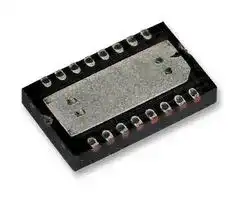
- No. of Pins: 16Pins
- Channel Type: N Channel
- Product Range: -
- Power Dissipation: 65.7W
- Transistor Mounting: Surface Mount
- Transistor Case Style: DFN
- Operating Frequency Max: 941MHz
- Operating Frequency Min: 136MHz
- Drain Source Voltage Vds: 30VDC
- Operating Temperature Max: 150°C
- Continuous Drain Current Id: -
| Delivery and price | |
|---|---|
| Units per pack | 1000 |
| Price | 1.82 € |
| Current stock | 10+ |
| Lead time | 30 days |
**NXP Semiconductors** Technical Data

Document Number: AFM907N Rev. 0, 04/2017

## **RF Power LDMOS Transistor**

## High Ruggedness N--Channel Enhancement--Mode Lateral MOSFET

Designed for handheld two--way radio applications with frequencies from 136 to 941 MHz. The high gain, ruggedness and wideband performance of this device make it ideal for large--signal, common--source amplifier applications in handheld radio equipment.

## **Wideband Performance** (In 350–520 MHz reference circuit, 7.5 Vdc, TA = 25°C, CW)

|**Frequency**<br>**(MHz) (1)**|||**Pin**<br>**(W)**|**Pin**<br>**(W)**||**Gps**<br>**(dB)**||η**D**<br>**(%)**||**Pout**<br>**(W)**|
|---|---|---|---|---|---|---|---|---|---|---|
|350|||0.25|||15.2||56.6||8.4|
|435|||0.25|||15.5||61.5||8.9|
|520|||0.25|||15.0||64.2||7.9|
|**Narrowband Performance** (7.5 Vdc, T|||(7.5 Vdc, TA= 25°C, CW)||||||||
|**Frequency**|||**Gps**|||η**D**||||**Pout**|
|**(MHz)**|||**(dB)**|||**(%)**||||**(W)**|
|520 **(2)**|||20.7|||73.9||||8.4|
|**Load Mismatch/Ruggedness**|||||||||||
|**Frequency**<br>**(MHz)**<br>**Signal**<br>**Type**|**VSWR**||||**Pin**<br>**(dBm)**|||**Test**<br>**Voltage**||**Result**|
|520 **(2)**<br>CW|> 65:1 at all<br>Phase Angles|||21<br>(3 dB Overdrive)||||10.8||No Device<br>Degradation|


## **Narrowband Performance** (7.5 Vdc, TA = 25°C, CW)

## **Load Mismatch/Ruggedness**

1. Measured in 350–520 MHz UHF broadband reference circuit (page 5).

2. Measured in 520 MHz narrowband RF test fixture (page 9).

## **Features**

- Characterized for operation from 136 to 941 MHz

- Unmatched input and output allowing wide frequency range utilization

- Integrated ESD protection

- Integrated stability enhancements

- Wideband — full power across the band

- Exceptional thermal performance

## **AFM907N**

**136–941 MHz, 8 W, 7.5 V WIDEBAND AIRFAST RF POWER LDMOS TRANSISTOR**

**DFN 4** × **6**

**==> picture [157 x 115] intentionally omitted <==**

**----- Start of picture text -----**<br>
N.C.N.C. 12 I@r——4 +|J&+ 1165 N.C.N.C.<br>Gate 3 3 14 Drain<br>Gate 4 7 | I cC 13 Drain<br>|<br>Gate 5 aa [|] J| .+ 12 Drain<br>Gate 6 a | I c 11 Drain<br>N.C. 7 1 | l r 10 N.C.<br>5 LLL 6<br>N.C. 8 L 9 N.C.<br>**----- End of picture text -----**<br>


(Top View)

Note: Exposed backside of the package is the source terminal for the transistor.

## **Figure 1. Pin Connections**

- Extreme ruggedness

- High linearity for: TETRA, SSB

## **Typical Applications**

- Output stage VHF band handheld radio

- Output stage UHF band handheld radio

- Output stage for 700–800 MHz handheld radio

© 2017 NXP B.V.

**AFM907N**

RF Device Data NXP Semiconductors

1

**Table 1. Maximum Ratings**

|**Table 1. Maximum Ratings**|**Table 1. Maximum Ratings**|||||
|---|---|---|---|---|---|
|**Rating**||**Symbol**|**Value**||**Unit**|
|Drain--Source Voltage||VDSS|–0.5, +30||Vdc|
|Gate--Source Voltage||VGS|–6.0, +12||Vdc|
|Operating Voltage||VDD|7.5, +0||Vdc|
|Storage Temperature Range||Tstg|–65 to +150||°C|
|Case Operating Temperature Range||TC|–40 to +150||°C|
|Operating Junction Temperature **(1,2)**||TJ|–40 to +150||°C|
|Total Device Dissipation @ TC= 25°C<br>Derate above 25°C||PD|65.7<br>0.52||W<br>W/°C|
|**Table 2. Thermal Characteristics**||||||
|**Characteristic**||**Symbol**|**Value (2,3)**||**Unit**|
|Thermal Resistance, Junction to Case<br>Case Temperature 79°C, 7.4 W CW, 7.5 Vdc, IDQ= 100 mA, 520 MHz||RθJC|1.9||°C/W|
|**Table 3. ESD Protection Characteristics**||||||
|**Test Methodology**|||**Class**|||
|Human Body Model (per JESD22--A114)|||1C, passes 1000 V|||
|Charge Device Model (per JESD22--C101)|||C3, passes 2000 V|||
|**Table 4. Moisture Sensitivity Level**||||||
|**Test Methodology**|**Rating**|**Package Peak Temperature**|||**Unit**|
|Per JESD22--A113, IPC/JEDEC J--STD--020|3||260||°C|
|**Table 5. Electrical Characteristics** (TA= 25°C unless otherwise noted)||||||
|**Characteristic**|**Symbol**|**Min**|**Typ**|**Max**|**Unit**|
|**Off Characteristics**||||||
|Zero Gate Voltage Drain Leakage Current<br>(VDS= 30 Vdc, VGS= 0 Vdc)|IDSS|—|—|10|μAdc|
|Zero Gate Voltage Drain Leakage Current<br>(VDS= 7.5 Vdc, VGS= 0 Vdc)|IDSS|—|—|2|μAdc|
|Gate--Source Leakage Current<br>(VGS= 5 Vdc, VDS= 0 Vdc)|IGSS|—|—|1|nAdc|
|**On Characteristics**||||||
|Gate Threshold Voltage<br>(VDS= 10 Vdc, ID= 110μAdc)|VGS(th)|1.6|2.1|2.6|Vdc|
|Drain--Source On--Voltage<br>(VGS= 10 Vdc, ID= 1.1 Adc)|VDS(on)|—|0.12|—|Vdc|
|Forward Transconductance<br>(VDS= 7.5 Vdc, ID= 3 Adc)|gfs|—|9.8|—|S|
|**Dynamic Characteristics**||||||
|Reverse Transfer Capacitance<br>(VDS= 7.5 Vdc±30 mV(rms)ac @ 1 MHz, VGS= 0 Vdc)|Crss|—|2.4|—|pF|
|Output Capacitance<br>(VDS= 7.5 Vdc±30 mV(rms)ac @ 1 MHz, VGS= 0 Vdc)|Coss|—|55.2|—|pF|
|Input Capacitance<br>(VDS= 7.5 Vdc, VGS= 0 Vdc±30 mV(rms)ac @ 1 MHz)|Ciss|—|95.7|—|pF|


1. Continuous use at maximum temperature will affect MTTF.

2. MTTF calculator available at http://www.nxp.com/RF/calculators.

3. Refer to AN1955 _, Thermal Measurement Methodology of RF Power Amplifiers._ Go to http://www.nxp.com/RF and search for AN1955. (continued)

**AFM907N**

RF Device Data NXP Semiconductors

2

**Table 5. Electrical Characteristics** (TA = 25°C unless otherwise noted) **(continued)**

|**Characteristic**|**Characteristic**|**Characteristic**|**Characteristic**|**Characteristic**|**Symbol**|**Min**|**Typ**||**Max**|**Unit**|
|---|---|---|---|---|---|---|---|---|---|---|
|**Narrowband Performance – 520 MHz**(In NXP Narrowband 520 MHz RF Test Fixture,<br>Pin= 18.5 dBm, f = 520 MHz||||||50 ohm system) VDD=||7.5|Vdc, IDQ= 100 mA,||
|Common--Source Amplifier Output Power|||||Pout|—|8.4||—|W|
|Drain Efficiency|||||ηD|—|73.9||—|%|
|**Load Mismatch/Ruggedness**(In NXP Narrowband 520 MHz RF Test Fixture, 50 ohm system) IDQ=|||||||100 mA||||
|**Frequency**<br>**(MHz)**|**Signal**<br>**Type**||**VSWR**|**Pin**<br>**(dBm)**||**Test Voltage, VDD**|||**Result**||
|520|CW||> 65:1 at all Phase Angles|21<br>(3 dB Overdrive)||10.8|||No Device Degradation||
|**Table 6. Ordering Information**|||||||||||
|**Device**||**Tape and Reel Information**|||||||**Package**||
|AFM907NT1||T1 Suffix = 1,000 Units, 16 mm Tape Width, 7--inch||||Reel|DFN 4×|6|||


**AFM907N**

RF Device Data NXP Semiconductors

3

## **TYPICAL CHARACTERISTICS**

**==> picture [239 x 171] intentionally omitted <==**

**----- Start of picture text -----**<br>
100<br>Ciss<br>C oss<br>Measured with ±30 mV(rms)ac @ 1 MHz, VGS = 0 Vdc<br>10<br>Crss<br>1<br>0 2 4 6 8 10 12 14<br>VDS, DRAIN--SOURCE VOLTAGE (VOLTS)<br>C, CAPACITANCE (pF)<br>**----- End of picture text -----**<br>


**Figure 2. Capacitance versus Drain--Source Voltage**

**==> picture [237 x 212] intentionally omitted <==**

**----- Start of picture text -----**<br>
10 [9]<br>VDD = 7.5 Vdc<br>10 [8] ID = 1.1 Amps<br>1.5 Amps<br>10 [7]<br>1.8 Amps<br>10 [6]<br>90 100 110 120 130 140 150 160<br>TJ, JUNCTION TEMPERATURE (°C)<br>Note:  MTTF value represents the total cumulative operating time<br>under indicated test conditions.<br>MTTF calculator available at http://www.nxp.com/RF/calculators.<br>MTTF (HOURS)<br>**----- End of picture text -----**<br>


**Figure 3. MTTF versus Junction Temperature – CW**

**AFM907N**

RF Device Data NXP Semiconductors

4

## **350–520 MHz UHF BROADBAND REFERENCE CIRCUIT**

**Table 7. 350–520 MHz UHF Broadband Performance** (In NXP UHF Broadband Reference Circuit, 50 ohm system) VDD = 7.5 Vdc, IDQ = 200 mA, TA = 25°C, CW

|50 ohm system) VDD= 7.5|Vdc, IDQ= 200 mA,|TA= 25°C, CW|||
|---|---|---|---|---|
|**Frequency**<br>**(MHz)**|**Pin**<br>**(W)**|**Gps**<br>**(dB)**|η**D**<br>**(%)**|**Pout**<br>**(W)**|
|350|0.25|15.2|56.6|8.4|
|435|0.25|15.5|61.5|8.9|
|520|0.25|15.0|64.2|7.9|


**AFM907N**

RF Device Data NXP Semiconductors

5

## **350--520 MHz UHF BROADBAND REFERENCE CIRCUIT — 0.83** ″ × **1.88** ″ **(21.1 mm** × **47.8 mm)**

|**350--520 MHz UHF BROADBAND REFERENCE CIRCUIT — 0.83**″ × **1.88**″**(21.1 mm** ×**47.8 mm)**|**350--520 MHz UHF BROADBAND REFERENCE CIRCUIT — 0.83**″ × **1.88**″**(21.1 mm** ×**47.8 mm)**|**350--520 MHz UHF BROADBAND REFERENCE CIRCUIT — 0.83**″ × **1.88**″**(21.1 mm** ×**47.8 mm)**|**350--520 MHz UHF BROADBAND REFERENCE CIRCUIT — 0.83**″ × **1.88**″**(21.1 mm** ×**47.8 mm)**|
|---|---|---|---|
|**Figure 4. AFM907N UHF Broadband Reference Circuit Component Layout — 350–520 MHz**<br>C7<br>C14<br>C1<br>C2<br>L1<br>L2<br>C4<br>C5<br>R1<br>R2<br>R3<br>B1<br>C6<br>C13<br>L4<br>L3<br>C16<br>C15<br>L6<br>L5<br>C8 C9<br>AFM907N<br>Rev. 0<br>C10<br>C3<br>J1<br>D93169<br>Q1<br>C12<br>C11<br>**Table 8. AFM907N UHF Broadband Reference Circuit Component Designations and Values — 350–520 MHz**||||
|**Part**|**Description**|**Part Number**|**Manufacturer**|
|B1|30Ω, 6 A Ferrite Bead|MPZ2012S300AT000<br>T|DK|
|C1, C12|100 pF Chip Capacitor|ATC600F101JT250XT<br>A|TC|
|C2|8.2 pF Chip Capacitor|ATC600F8R2BT250XT<br>A|TC|
|C3, C5|36 pF Chip Capacitor|ATC600F360JT250XT<br>A|TC|
|C4, C8, C9|27 pF Chip Capacitor|ATC600F270JT250XT<br>A|TC|
|C6|1μF Chip Capacitor|GRM21BR71H105KA12L<br>M|urata|
|C7|0.01μF Chip Capacitor|C0805C103K5RAC<br>K|emet|
|C10|18 pF Chip Capacitor|ATC600F180JT250XT<br>A|TC|
|C11|9.1 pF Chip Capacitor|ATC600F9R1BT250XT<br>A|TC|
|C13|240 pF Chip Capacitor|ATC600F241JT250XT<br>A|TC|
|C14|2.2μF Chip Capacitor|GRM31CR71H225KA88L<br>M|urata|
|C15|4.7μF 50 V Chip Capacitor|GRM31CR71H475KA12L<br>M|urata|
|C16|0.01μF Chip Capacitor|GRM21BR72A103KA01B<br>M|urata|
|J1|Right-Angle Breakaway Header (3 Pins)|22-28-8360<br>M|olex|
|L1, L6|8.9 nH Inductor|0806SQ8N9<br>C|oilcraft|
|L2|1.65 nH Inductor, 2 Turns|0906-2JLC<br>C|oilcraft|
|L3, L4|17 nH Inductor|0908SQ17N<br>C|oilcraft|
|L5|2.55 nH Inductor, 3 Turns|0906-3JLC<br>C|oilcraft|
|Q1|RF Power LDMOS Transistor|AFM907N<br>N|XP|
|R1, R2|1.5Ω, 1/4 W Chip Resistor|RC1206FR-071R5L<br>Y|ageo|
|R3|51Ω, 1/4 W Chip Resistor|CRCW120651R0FKEA<br>V|ishay|
|PCB|Shengyi S1000--2, 0.020″,εr = 4.8|D93169<br>M|TL|


**AFM907N**

RF Device Data NXP Semiconductors

6

## **TYPICAL CHARACTERISTICS — 350–520 MHz UHF BROADBAND REFERENCE CIRCUIT**

**==> picture [459 x 589] intentionally omitted <==**

**----- Start of picture text -----**<br>
25 70<br>23 60<br>ηD<br>21 50<br>19 40<br>17 30<br>Gps<br>15 14<br>13 12<br>11 P out 10<br>9 8<br>7 6<br>VDD = 7.5 Vdc, Pin = 0.25 W, IDQ = 200 mA<br>5 4<br>340 360 380 400 420 440 460 480 500 520 540<br>f, FREQUENCY (MHz)<br>Figure 5. Power Gain, Drain Efficiency and Output Power<br>versus Frequency at a Constant Input Power<br>10<br>VDD = 7.5 Vdc 1.2<br>f= 435 MHz VDD = 7.5 Vdc<br>8 1.0 f = 435 MHz<br>Pin = 24 dBm<br>0.8<br>6<br>Pin = 24 dBm<br>0.6<br>4 P in = 21 dBm 0.4<br>Pin = 21 dBm<br>0.2<br>2<br>Detail A 0<br>0 0.5 1.0 1.5 2.0 2.5<br>0<br>0 0.5 1.0 1.5 2.0 2.5 3.0 3.5 4.0 VGS, GATE--SOURCE VOLTAGE (VOLTS)<br>VGS, GATE--SOURCE VOLTAGE (VOLTS) Detail A<br>Figure 6. Output Power versus Gate--Source Voltage<br>25 90<br>520 MHz<br>23 70<br>ηD<br>21 50<br>435 MHz 350 MHz<br>19 30<br>17 10<br>Gps<br>15 12<br>350 MHz<br>435 MHz<br>13 Pout 9<br>520 MHz<br>11 435 MHz 6<br>350 MHz<br>9 3<br>520 MHz VDD = 7.5 Vdc, IDQ = 200 mA<br>7 0<br>0 0.05 0.10 0.15 0.20 0.25 0.30 0.35<br>Pin, INPUT POWER (WATTS)<br>, DRAIN<br>D<br>η<br>EFFICIENCY (%)<br>, POWER GAIN (dB)<br>ps<br>G<br>, OUTPUT<br>out<br>P<br>POWER (WATTS)<br>, OUTPUT POWER (WATTS)<br>, OUTPUT POWER (WATTS)<br>out<br>out P<br>P<br>, DRAIN<br>D<br>η<br>EFFICIENCY (%)<br>, POWER GAIN (dB)<br>ps<br>G<br>, OUTPUT<br>out<br>P<br>POWER (WATTS)<br>**----- End of picture text -----**<br>


**Figure 7. Power Gain, Drain Efficiency and Output Power versus Input Power and Frequency**

**AFM907N**

RF Device Data NXP Semiconductors

7

## **350–520 MHz BROADBAND REFERENCE CIRCUIT**

**==> picture [466 x 647] intentionally omitted <==**

**----- Start of picture text -----**<br>
hy Jo Zo = 5 Ω<br>BOX < Coe oH TAL \<br>ATASft/sSH IEbyEOLPRERORO $ LRRDRE Zsource x aren>+ f = 520 MHz soemSO;x aSeYlEH LINTPALKTsx)<br>Sls]f/f ShTS LEER R EP LIQ LR REDO SS NLR<br>fs] f = 350 MHz LIN SS SSTLEERY<br>£foh fe{J RByk i  SHERsieeeeedfatentansLe)feesTy op cre ERECLPIPTPREROCKIL ORRSIRR S SEty esa2<br>1] lef fi ieee sage EP PET EERE OSE12<br>S E f = 520 MHz aieA<br>PMR Ria<br>sseeteieesitiiae ener" bis beatae ta ni mae [ae]<br>| = PCA wed " OR CONCUCTANCE COMPONENT cl mas Hit 7. iS<br>Zload f = 350 MHz<br>ol Lee ctsA re SS<br>ES e e  SSSSS oR CS<br>a\e\ | VeCS Se SP RRL Gaia a)<br>AREWX oemeencain @<br>BBC ISRO T EE FESS<br>f Zsource Zload<br>MHz Ω Ω<br>350 1.9 + j1.6 3.1 -- j0.7<br>eeee<br>360 2.0 + j1.9 3.2 -- j0.6<br>ee ee<br>370 2.0 + j2.0 3.2 -- j0.5<br>eeee<br>380 2.1 + j2.2 3.3 -- j0.5<br>ee ee<br>390 2.2 + j2.4 3.3 -- j0.5<br>eeee<br>400 2.3 + j2.6 3.2 -- j0.5<br>ee ee<br>410 2.3 + j2.7 3.2 -- j0.5<br>ee ee<br>420 2.4 + j2.8 3.1 -- j0.6<br>ee ee<br>430 2.5 + j2.9 3.0 -- j0.6<br>ee ee<br>440 2.6 + j3.0 2.8 -- j0.6<br>es ee<br>450 2.7 + j3.1 2.7 -- j0.6<br>es ee<br>460 2.7 + j3.2 2.5 -- j0.6<br>ee ee<br>470 2.8 + j3.2 2.3 -- j0.5<br>es ee<br>480 2.9 + j3.3 2.1 -- j0.5<br>ee ee<br>490 3.0 + j3.4 2.0 -- j0.4<br>ee ee<br>500 3.0 + j3.4 1.8 -- j0.3<br>ee ee<br>510 3.1 + j3.5 1.7 -- j0.1<br>ee ee<br>520 3.2 + j3.5 1.5 + j0.04<br>ee ee<br>Zsource = Test circuit impedance as measured from<br>gate to ground.<br>Zload = Test circuit impedance as measured from<br>drain to ground.<br>Input Device Output<br>Matching Under Matching<br>Network Test Network<br>50 Ω 50 Ω<br>Zsource Zload<br>**----- End of picture text -----**<br>


**Figure 8. Broadband Series Equivalent Source and Load Impedance — 350–520 MHz**

**AFM907N**

RF Device Data NXP Semiconductors

8

**520 MHz NARROWBAND RF TEST FIXTURE — 5.0** ″ × **3.0** ″ **(12.70 cm** × **7.62 cm)**

|||**52**|**0 MH**|**z NARROWBAND**|**RF T**|**EST FIXTURE — 5.0**″ ×|**EST FIXTURE — 5.0**″ ×|**EST FIXTURE — 5.0**″ ×|**EST FIXTURE — 5.0**″ ×|**3.0**″**(12.70**|**3.0**″**(12.70**|**3.0**″**(12.70**|**cm** ×**7.62 cm)**|**cm** ×**7.62 cm)**|**cm** ×**7.62 cm)**|**cm** ×**7.62 cm)**||
|---|---|---|---|---|---|---|---|---|---|---|---|---|---|---|---|---|---|
|**Table 9.**||C|C3|B1|||||||||C13<br>C14<br>C9<br>C15|||||
||||1<br>C2|C4<br>C7<br>R||L||||C12<br>1||||||||
||||||1|||L||||||||||
|||||C5|||||||||L2||C11|||
|||||C6||||||||||||||
||||||||||||||||C10|||
||||||||||||||C8|||||
|||||||||||||||||||
|||||||||||||||||||
||||||||||||||AFM907N<br>Rev. 0|||||
|||||||||||||||||||
|||||||||||||||||||
||**AFM907N**||**Figure 9. AFM907N Narrowband RF Test Fixture Component Layout — 520 MHz**<br>**Narrowband RF Test Fixture Component Designations and Values — 520 MHz**|||||||||||||||
||**Part**|||**Description**|||||**Part Number**|||||||**Manufacturer**||
|B1||||Short RF Bead|||||2743019447|||||||Fair-Rite||
|C1||||22μF, 35 V Tantalum Capacitor|||||T491X226K035AT|||||||Kemet||
|C2, C14||||0.1μF Chip Capacitor|||||CDR33BX104AKWS|||||||AVX||
|C3, C13||||0.01μF Chip Capacitor|||||C0805C103K5RAC|||||||Kemet||
|C4, C12||||180 pF Chip Capacitor|||||ATC100B181JT300XT|||||||ATC||
|C5||||33 pF Chip Capacitor|||||ATC100B130JT500XT|||||||ATC||
|C6||||22 pF Chip Capacitor|||||ATC100B220JT500XT|||||||ATC||
|C7||||20 pF Chip Capacitor|||||ATC100B220JT500XT|||||||ATC||
|C8, C9||||16 pF Chip Capacitor|||||ATC100B160JT500XT|||||||ATC||
|C10||||2.7 pF Chip Capacitor|||||ATC100B2R7BT500XT|||||||ATC||
|C11||||30 pF Chip Capacitor|||||ATC100B300JT500XT|||||||ATC||
|C15||||330μF, 35 V Electrolytic Capacitor|||||MCGPR35V337M10X16-RH|||||||Multicomp||
|L1||||22 nH Inductor, 7 Turns|||||B07TJLC|||||||Coilcraft||
|L2||||5 nH Inductor, 2 Turns|||||A02TKLC|||||||Coilcraft||
|R1||||5.6Ω, 1/4 W Chip Resistor|||||CRCW12065R60FKEA|||||||Vishay||
|PCB||||Rogers RO4350B, 0.030″,εr = 3.66|||||D88764|||||||MTL||


**AFM907N**

RF Device Data NXP Semiconductors

9

## **TYPICAL CHARACTERISTICS — 520 MHz NARROWBAND RF TEST FIXTURE**

**==> picture [234 x 173] intentionally omitted <==**

**----- Start of picture text -----**<br>
12<br>VDD = 7.5 Vdc<br>f= 520 MHz<br>10<br>Pin = 18.5 dBm<br>8<br>Pin = 15.5 dBm<br>6<br>4<br>2<br>0<br>1.0 1.5 2.0 2.5 3.0 3.5 4.0<br>VGS, GATE--SOURCE VOLTAGE (VOLTS)<br>, OUTPUT POWER (WATTS)<br>out<br>P<br>**----- End of picture text -----**<br>


**Figure 10. Output Power versus Gate--Source Voltage**

**==> picture [282 x 174] intentionally omitted <==**

**----- Start of picture text -----**<br>
25 90<br>24 70<br>ηD<br>23 50<br>22 30<br>21 10<br>20 P out 12<br>19 10<br>18 8<br>17 6<br>Gps<br>16 4<br>15 2<br>VDD = 7.5 Vdc, IDQ1 = 100 mA, f = 520 MHz<br>14 0<br>0 0.05 0.10 0.15 0.20 0.25 0.30 0.35 0.40<br>Pin, INPUT POWER (WATTS)<br>, DRAIN<br>D<br>η<br>EFFICIENCY (%)<br>, POWER GAIN (dB)<br>ps<br>G<br>, OUTPUT<br>out<br>P<br>POWER (WATTS)<br>**----- End of picture text -----**<br>


**Figure 11. Power Gain, Drain Efficiency and Output Power versus Input Power**

**AFM907N**

RF Device Data NXP Semiconductors

10

**==> picture [465 x 189] intentionally omitted <==**

**----- Start of picture text -----**<br>
5.35 × 2.0 solder pad 2.00 3.00<br>with thermal via structure.<br>All dimensions in mm.<br>5.35<br>0.56<br>0.35 10 × 0.80 4 × 0.65<br>**----- End of picture text -----**<br>


**Figure 12. PCB Pad Layout for 16--Lead DFN 4** × **6**

**==> picture [132 x 173] intentionally omitted <==**

**----- Start of picture text -----**<br>
AFM907N<br>WLYW<br>**----- End of picture text -----**<br>


**Figure 13. Product Marking**

**AFM907N**

RF Device Data NXP Semiconductors

11

## **PACKAGE DIMENSIONS**

**==> picture [326 x 423] intentionally omitted <==**

**AFM907N**

RF Device Data NXP Semiconductors

12

**==> picture [504 x 39] intentionally omitted <==**

**==> picture [149 x 39] intentionally omitted <==**

**AFM907N**

RF Device Data NXP Semiconductors

13

**AFM907N**

RF Device Data NXP Semiconductors

14

## **PRODUCT DOCUMENTATION, SOFTWARE AND TOOLS**

Refer to the following resources to aid your design process.

## **Application Notes**

- AN1907: Solder Reflow Attach Method for High Power RF Devices in Over--Molded Plastic Packages

- AN1955: Thermal Measurement Methodology of RF Power Amplifiers

## **Engineering Bulletins**

- EB212: Using Data Sheet Impedances for RF LDMOS Devices

## **Software**

- Electromigration MTTF Calculator

- RF High Power Model

- .s2p File

## **Development Tools**

- Printed Circuit Boards

## **To Download Resources Specific to a Given Part Number:**

1. Go to http://www.nxp.com/RF

2. Search by part number

3. Click part number link

4. Choose the desired resource from the drop down menu

## **REVISION HISTORY**

The following table summarizes revisions to this document.

|**Revision**|**Date**|**Description**|
|---|---|---|
|0|Apr. 2017|•<br>Initial release of data sheet|


**AFM907N**

RF Device Data NXP Semiconductors

15

## _**How to Reach Us:**_

**Home Page:** nxp.com

**Web Support:** nxp.com/support

Information in this document is provided solely to enable system and software implementers to use NXP products. There are no express or implied copyright licenses granted hereunder to design or fabricate any integrated circuits based on the information in this document. NXP reserves the right to make changes without further notice to any products herein.

NXP makes no warranty, representation, or guarantee regarding the suitability of its products for any particular purpose, nor does NXP assume any liability arising out of the application or use of any product or circuit, and specifically disclaims any and all liability, including without limitation consequential or incidental damages. “Typical” parameters that may be provided in NXP data sheets and/or specifications can and do vary in different applications, and actual performance may vary over time. All operating parameters, including “typicals,” must be validated for each customer application by customer’s technical experts. NXP does not convey any license under its patent rights nor the rights of others. NXP sells products pursuant to standard terms and conditions of sale, which can be found at the following address: nxp.com/SalesTermsandConditions.

NXP, the NXP logo, Freescale, the Freescale logo, and Airfast are trademarks of NXP B.V. All other product or service names are the property of their respective owners. E 2017 NXP B.V.

**AFM907N**

RF Device Data NXP Semiconductors

Document Number: AFM907N 16Rev. 0, 04/2017
Updated at April 10, 2026
NXP Semiconductors is a global leader in secure connectivity solutions, driving innovation across the automotive, industrial, IoT, mobile, and communications infrastructure markets. By developing advanced, purpose-built technologies, NXP enables devices to sense, think, connect, and act intelligently, delivering rigorously tested components that make the connected world safer and more efficient. Within the semiconductor space, NXP is highly regarded for its extensive range of high-performance integrated circuits and discrete devices. The brand's portfolio excels in drivers and interfaces, featuring a comprehensive selection of I/O expanders designed to streamline complex system architectures. For demanding high-frequency and wireless applications, NXP provides industry-leading RF FETs and RF/PIN diodes engineered to deliver exceptional signal integrity, efficiency, and reliability. The NXP product lineup further extends to essential discrete components, including versatile bipolar transistors, JFETs, and small signal diodes optimized for precision switching and amplification. Additionally, the portfolio supports advanced automation and smart applications with precision IC sensors, such as MEMS accelerometers, alongside specialized power management solutions like AC/DC LED driver ICs and single MOSFETs for cutting-edge electronics design.
About Novapart
Novapart is a B2B electronic component broker specialising in stock shortages and cost reduction. We source hard-to-find parts and identify compliant alternatives across a catalogue of 540,000+ components from 500+ manufacturers.
Learn more →Stock Shortage Specialist
When a component is unavailable, discontinued or has an unacceptable lead time, we tap into our network of vetted European and Asian distributors to source what you need — without compromising on quality or traceability.
Request a quote →Compliant Alternatives
We identify pin-to-pin, electrically equivalent substitutes that meet the same certifications (RoHS, AEC-Q100, REACH) as your original specification — validated against datasheets, not just part numbers. Often at a lower cost.
BOM Analysis service →