


ACST410-8FP
Triac, ACST4 Series, 800 V, 4 A, TO-220FPAB, 1 V, 30 A, 20 mA
- Manufacturer: STMICROELECTRONICS
- Product type:
- Peak Repetitive Off-State Voltage, Vdrm:800V; On State RMS Current IT(rms):4A; Triac Case Style:TO-220FPAB; Gate Trigger Current Max (QI), Igt:10mA; Gate Trigger Voltage Max Vgt:
- MSL: -
- SVHC: No SVHC (25-Jun-2025)
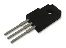
- No. of Pins: 3Pins
- Product Range: -
- Triac Case Style: TO-220FPAB
- Thyristor Mounting: Through Hole
- Holding Current Max: 20mA
- On State RMS Current: 4A
- Peak On State Voltage: 1.7V
- Gate Trigger Voltage Max: 1V
- Operating Temperature Max: 125°C
- Peak Non Repetitive Surge Current: 30A
- Peak Repetitive Off State Voltage: 800V
| Delivery and price | |
|---|---|
| Units per pack | 1000 |
| Price | 0.448 € |
| Current stock | 50+ |
| Lead time | 30 days |
**ACST4**

Datasheet

## 4 A - 800 V overvoltage protected AC switch

## **Features**

**==> picture [140 x 65] intentionally omitted <==**

**----- Start of picture text -----**<br>
OUT<br>COM G<br>OUT<br>G COM<br>DPAK TO-220FPAB<br>**----- End of picture text -----**<br>


- Triac with overvoltage protection

- Low IGT (<10 mA) or high immunity (IGT < 35 mA) version

- High noise immunity: static dV/dt > 1000 V/μs

- TO-220FPAB insulated package:

   - complies with UL standards (File ref : E81734)

**==> picture [84 x 95] intentionally omitted <==**

**----- Start of picture text -----**<br>
OUT<br>G<br>COM<br>**----- End of picture text -----**<br>


   - insulation voltage: 2000 VRMS

- Benefits:

   - Enables equipment to meet IEC 61000-4-5

   - High off-state reliability with planar technology

   - Needs no external overvoltage protection

   - Reduces the power passive component count

   - High immunity against fast transients described in IEC 61000-4-4 standards

## **Applications**

- AC mains static switching in appliance and industrial control systems

- Drive of medium power AC loads such as:

   - Universal drum motor of washing machine

   - Compressor of fridge or air conditioner

## **Product status link**

|**Product status link**|**Product status link**|
|---|---|
|ACST4||
|||
|**Product summary**||
|**IT(RMS)**|4 A|
|**VDRM/VRRM**|800 V|
|**IGT (ACST410)**|10 mA|
|**IGT (ACST435)**|35 mA|


## **Description**

The ACST4 series belongs to the ACS / ACST power switch family. This high performance device is suited to home appliances or industrial systems and drives loads up to 4 A.

This ACST4 switch embeds a Triac structure with a high voltage clamping device to absorb the inductive turn-off energy and withstand line transients such as those described in the IEC 61000-4-5 standards. The ACST410 needs a low gate current to be activated (IGT < 10 mA) and still shows a high electrical noise immunity complying with IEC standards such as IEC 61000-4-4 (fast transient burst test).

**DS2762** - **Rev 12** - **August 2021** For further information contact your local STMicroelectronics sales office.

www.st.com

**ACST4 Characteristics**

## **1 Characteristics**

**Table 1. Absolute ratings (limiting values)**

|**Symbol**|**Parameter**|||**Value**|**Unit**|
|---|---|---|---|---|---|
|IT(RMS)|On-state rms current (full sine wave)|TO-220FPAB|Tc= 102 °C|4|A|
|||DPAK|Tc= 112 °C|||
|||DPAK with 0.5 cm copper|Tamb= 60 °C|1||
|ITSM|Non repetitive surge peak on-state current<br>Tjinitial = 25 °C, (full cycle sine wave)|f = 50 Hz|tp= 20 ms|32|A|
|||f = 60 Hz|tp= 16.7 ms|30||
|I2t|I2t for fuse selection||tp= 10 ms|6|A2s|
|dI/dt|Critical rate of rise on-state current IG= 2 x IGT, tr ≤<br>100 ns|f = 120 Hz|Tj= 125 °C|100|A/μs|
|VPP(1)|Non repetitive line peak pulse voltage(1)||Tj= 25 °C|2|kV|
|PG(AV)|Average gate power dissipation||Tj= 125 °C|0.1|W|
|PGM|Peak gate power dissipation (tp= 20 μs)||Tj= 125 °C|10|W|
|IGM|Peak gate current (tp= 20 μs)||Tj= 125 °C|1.6|A|
|Tstg|Storage temperature range|||-40 to +150|°C|
|Tj|Operating junction temperature range|||-40 to +125|°C|
|TL|Lead temperature for soldering during 10 s (at 3 mm from plastic case)|||260|°C|
|Vins|Insulation rms voltage (60 seconds)|||2000|V|


_1. according to test described by standard IEC 61000-4-5, see Figure 17 for conditions_

**Table 2. Electrical characteristics (Tj = 25 °C, unless otherwise specified)**

|**Sbl**|**Tt diti**|**Qdt**||**Value**|**Value**|**Uit**|
|---|---|---|---|---|---|---|
|**ymo**|**es conons**|**uaran**||**ACST410**|**ACST435**|**n**|
|IGT (1)|VOUT= 12 V, RL= 33 Ω|I - II - III|Max.|10|35|mA|
|VGT|||Max.|1.0|1.1|V|
|VGD|VOUT= VDRM, RL= 3.3 kΩ, Tj= 125 °C|I - II - III|Min.|0.2||V|
|IH(2)|IOUT= 500 mA||Max.|20|25|mA|
|IL|IG= 1.2 x IGT|I - II - III|Max.|40|60|mA|
|dV/dt(2)|VOUT= 67% VDRM, gate open, Tj= 125 °C||Min.|500|1000|V/μs|
|(dI/dt)c(2)|Without snubber, Tj= 125 °C||Min.||5|A/ms|
|(dI/dt)c(2)|(dV/dt)c = 15 V/μs, Tj= 125 °C||Min.|2||A/ms|
|VCL|ICL= 0.1 mA, tp= 1 ms||Min.|850||V|


_1. Minimum IGT is guaranteed at 5% of IGT max_

_2. For both polarities of OUT pin referenced to COM pin_

**DS2762** - **Rev 12**

**page 2/16**

**ACST4 Characteristics**

## **Table 3. Static characteristics**

|**Symbol**|**Test conditions**|**Test conditions**|**Test conditions**|**Value**|**Unit**|
|---|---|---|---|---|---|
|VTM (1)|IOUT= 5.6 A, tp= 500 μs|Tj= 25 °C|Max.|1.7|V|
|VT0(1)|Threshold voltage|Tj= 125 °C|Max.|0.9|V|
|RD(1)|Dynamic resistance|Tj= 125 °C|Max.|110|mΩ|
|IDRM<br>IRRM|VOUT= VDRM/ VRRM|Tj= 25 °C|Max.|20|µA|
|||Tj= 125 °C||0.5|mA|


_1. For both polarities of OUT pin referenced to COM pin_

## **Table 4. Thermal characteristics**

|**Symbol**|**Parameter**||**Value**|**Unit**|
|---|---|---|---|---|
|Rth(j-c)|Junction to case for full cycle sine wave conduction|DPAK|2.6|°C/W|
|||TO-220FPAB|4.6||
|Rth(j-a)|Junction to ambient|TO-220FPAB|60||
||Junction to ambient, SCU= 0.5 cm²(1)|DPAK|70||


_1. SCU = copper surface under tab_

**DS2762** - **Rev 12**

**page 3/16**

**ACST4 Characteristics (curves)**

## **1.1 Characteristics (curves)**

**==> picture [513 x 622] intentionally omitted <==**

**----- Start of picture text -----**<br>
Figure 1. Maximum power dissipation versus RMS on- Figure 2. On-state RMS current versus case temperature<br>state current (full cycle)<br>P(W) IT(RMS) (A)<br>6 α = 180° 180° 5<br>α=180°<br>5 DPAK<br>4<br>TO220FPAB<br>4<br>3<br>3<br>2<br>2<br>1 1<br>TC (°C)<br>IT(RMS)(A)<br>0 0<br>0.0 0.5 1.0 1.5 2.0 2.5 3.0 3.5 4.0 0 25 5 0 75 100 125<br>Figure 3. On-state RMS current versus ambient Figure 4. Relative variation of thermal impedance junction<br>temperature (free air convection, full cycle) to case versus pulse duration<br>IT(RMS) (A) K = [Zth / Rth]<br>2.0 1.0E+00<br>α=180° Zth(j-c)<br>TO-220FPAB DPAK Zth(j-a)<br>1.5<br>DPAK with copper<br>surface = 0.5 cm [2]<br>1.0 1.0E-01 TO-220FPAB<br>0.5<br>Ta(°C) Tp(s)<br>0.0 1.0E-02<br>0 25 50 75 100 125 1.0E-03 1.0E-02 1.0E-01 1.0E+00 1.0E+01 1.0E+02 1.0E+03<br>Figure 5. Relative variation of gate trigger current and Figure 6. Relative variation of holding current and<br>gate trigger voltage versus junction temperature (typical latching current versus junction temperature (typical<br>values) values)<br>IGT,VGT[Tj] / IGT,VGT[Tj = 25 °C] IH,IL[Tj] / IH,IL[Tj = 25 °C]<br>3.0<br>2.5<br>2.5 IGT Q3<br>2.0<br>2.0 IGT Q1-Q2<br>1.5<br>1.5<br>1.0 VGT Q1-Q2-Q3 1.0<br>IL<br>0.5 0.5 IH<br>Tj(°C)<br>0.0 Tj(°C)<br>0.0<br>-50 -25 0 25 50 75 100 125<br>-50 -25 0 25 50 75 100 125<br>**----- End of picture text -----**<br>


**DS2762** - **Rev 12**

**page 4/16**

**ACST4 Characteristics (curves)**

**==> picture [513 x 191] intentionally omitted <==**

**----- Start of picture text -----**<br>
Figure 7. Surge peak on-state current versus number of Figure 8. Non repetitive surge peak on-state current for a<br>cycles sinusoidal pulse width<br>ITSM (A) ITSM(A), (A²s)<br>35 1000<br>dl/dt limitation: 100 A / µs Tj initial = 25 °C<br>30<br>t=20ms<br>25<br>20 TNon repetitivej initial=25 °C One cycle 100 ITSM<br>15<br>10<br>10<br>Repetitive<br>5 TC=102°C<br>0 Number of cycles 1 tp (ms)<br>1 10 100 1000 0.01 0.10 1.00 10.00<br>**----- End of picture text -----**<br>


**Figure 9. On-state characteristics (maximum values)**

**==> picture [222 x 142] intentionally omitted <==**

**----- Start of picture text -----**<br>
ITM (A)<br>100<br>Tjmax:<br>Vto = 0.90 V<br>Rd = 110 mΩ<br>10<br>Tj = 125 °C<br>1 Tj = 25 °C VTM (V)<br>0 1 2 3 4 5<br>**----- End of picture text -----**<br>


**Figure 10. Relative variation of critical rate of decrease of main current (dI/dt)c versus junction temperature**

**==> picture [224 x 141] intentionally omitted <==**

**----- Start of picture text -----**<br>
(dI/dt) c [Tj] / (dl/dt) c [Tj = 125 °C]<br>8<br>7<br>6<br>5<br>4<br>3<br>2<br>1<br>0 Tj(°C)<br>25 50 75 100 125<br>**----- End of picture text -----**<br>


**Figure 11. Relative variation of static dV/dt immunity versus junction temperature (gate open)**

**==> picture [224 x 140] intentionally omitted <==**

**----- Start of picture text -----**<br>
dV/dt [T j] / dV/dt [T j = 125 °C]<br>6<br>VD = VR = 536 V<br>5<br>4<br>3<br>2<br>1<br>0 Tj(°C)<br>25 50 75 100 125<br>**----- End of picture text -----**<br>


**Figure 12. Relative variation of Leakage current versus junction temperature**

**==> picture [226 x 144] intentionally omitted <==**

**----- Start of picture text -----**<br>
IDRM/IRRM [Tj; VDRM / VRRM] / IDRM/IRRM [Tj = 125 °C; 800 V]<br>1.0E+00<br>VDRM = VRRM = 800V<br>Different bloc king voltages<br>1.0E-01<br>VDRM = VRRM = 600 V<br>1.0E-02<br>VDRM = VRRM = 200 V<br>Tj(°C)<br>1.0E-03<br>25 50 75 100 125<br>**----- End of picture text -----**<br>


**DS2762** - **Rev 12**

**page 5/16**

**ACST4 Characteristics (curves)**

**==> picture [513 x 191] intentionally omitted <==**

**----- Start of picture text -----**<br>
Figure 13. Relative variation of the clamping voltage Figure 14. Thermal resistance junction to ambient versus<br>versus junction temperature (minimum values) copper surface under tab (typical values)<br>1.15 VCL[ Tj] /V CL [Tj = 25 °C] Rth(j-a) (°C/W)<br>100<br>DPAK<br>90 Epoxy printed circuit board, copper thickness: 35 µm<br>1.10<br>80<br>1.05 70<br>60<br>1.00 50<br>40<br>0.95 30<br>20<br>0.90<br>10<br>S Cu (cm²)<br>0.85 Tj(°C) 0<br>0 5 10 15 20 25 30 35 40<br>-50 -25 0 25 50 75 100 125<br>**----- End of picture text -----**<br>


**DS2762** - **Rev 12**

**page 6/16**

**ACST4 Application information**

## **2 Application information**

## **2.1 Typical application descriptions**

The ACST4 device has been designed to control medium power load, such as AC motors in home appliances. Thanks to its thermal and turn off commutation performances, the ACST4 switch is able to drive an inductive load up to 4 A with no turn off additional snubber. It also provides high thermal performances in static and transient modes such as the compressor inrush current or high torque operating conditions of an AC motor. Thanks to its low gate triggering current level, the ACST4 can be driven directly by an MCU through a simple gate resistor as shown Figure 15 and Figure 16.

**Figure 15. Compressor control – typical diagrams**

**==> picture [420 x 255] intentionally omitted <==**

**----- Start of picture text -----**<br>
Compressor Compressor<br>AC Mains<br>PTC AC Mains<br>Electronic PTC<br>ACST<br>starter<br>1 logical circuitry ACST<br>Start<br>switch<br>ACST<br>Run<br>switch<br>Electronic<br>ACST thermostat<br>Rg<br>Rg Rg<br>Gate Gate<br>Power supply Driver Power supply Driver<br>Compressor with integrated e-starter Compressor with external electronic drive<br>2<br>3<br>**----- End of picture text -----**<br>


**DS2762** - **Rev 12**

**page 7/16**

**ACST4 Typical application descriptions**

**Figure 16. Universal drum motor control – typical diagram**

**==> picture [257 x 272] intentionally omitted <==**

**----- Start of picture text -----**<br>
Universal motor<br>Stator Rotor<br>12V<br>AC Mains<br>Motor direction<br>setting<br>MCU<br>Speed motor ACST Rg<br>regulation<br>Vcc<br>MCU<br>**----- End of picture text -----**<br>


**DS2762** - **Rev 12**

**page 8/16**

**ACST4**

**AC line transient voltage ruggedness**

## **2.2 AC line transient voltage ruggedness**

In comparison with standard Triacs, which are not robust against surge voltage, the ACST4 is self-protected against over-voltage, specified by the new parameter VCL. The ACST4 switch can safely withstand AC line transient voltages either by clamping the low energy spikes, such as inductive spikes at switch off, or by switching to the on state (for less than 10 ms) to dissipate higher energy shocks through the load. This safety feature works even with high turn-on current ramp up.

The test circuit of represents the ACST4 application, and is used to stress the ACST switch according to the IEC 61000-4-5 standard conditions. With the additional effect of the load which is limiting the current, the ACST switch withstands the voltage spikes up to 2 kV on top of the peak line voltage. The protection is based on an overvoltage crowbar technology. The ACST4 folds back safely to the on state as shown in . The ACST4 recovers its blocking voltage capability after the surge and the next zero current crossing.

Such a non repetitive test can be done at least 10 times on each AC line voltage polarity.

## **Figure 17. Overvoltage ruggedness test circuit for resistive and inductive loads for IEC 61000-4-5 standards**

R = 23 Ω, L = 2 µH, Vsurge = 2 kV Rg = 220 Ω (ACST410-8), 68 Ω (ACST435-8)

**==> picture [385 x 189] intentionally omitted <==**

**----- Start of picture text -----**<br>
Surge generator<br>2kV surge<br>Rgene<br>Model of the load<br>Filtering unit<br>R L<br>ACST4<br>AC Mains<br>Rg<br>**----- End of picture text -----**<br>


**Figure 18. Typical voltage and current waveforms across the ACST4 during IEC 61000-4-5 standard test**

**==> picture [219 x 148] intentionally omitted <==**

**----- Start of picture text -----**<br>
Vpeak= VCL<br>1.2/50 µs voltage surge<br>V<br>0<br>Ipeak = 90 A 8/20 µs current surge<br>I<br>**----- End of picture text -----**<br>


**==> picture [138 x 20] intentionally omitted <==**

**----- Start of picture text -----**<br>
0<br>dI/dt = 130 A/µs<br>**----- End of picture text -----**<br>


**DS2762** - **Rev 12**

**page 9/16**

**ACST4 Package information**

## **3 Package information**

In order to meet environmental requirements, ST offers these devices in different grades of ECOPACK packages, depending on their level of environmental compliance. ECOPACK specifications, grade definitions and product status are available at: www.st.com. ECOPACK is an ST trademark.

## **3.1 TO-220FPAB package information**

- Epoxy meets UL94, V0

- Recommended torque: 0.4 to 0.6 N·m

**Figure 19. TO-220FPAB package outline**

**DS2762** - **Rev 12**

**page 10/16**

**ACST4**

**TO-220FPAB package information**

**Table 5. TO-220FPAB package mechanical data**

||**Dimensions**|**Dimensions**|**Dimensions**|**Dimensions**|
|---|---|---|---|---|
|**Ref.**|**Millimeters**||**Inches**||
||**Min.**|**Max.**|**Min.**|**Max.**|
|A|4.40|4.60|0.1739|0.1818|
|B|2.5|2.7|0.0988|0.1067|
|D|2.50|2.75|0.0988|0.1087|
|E|0.45|0.70|0.0178|0.0277|
|F|0.75|1.0|0.0296|0.0395|
|F1|1.15|1.70|0.0455|0.0672|
|F2|1.15|1.70|0.0455|0.0672|
|G|4.95|5.20|0.1957|0.2055|
|G1|2.40|2.70|0.0949|0.1067|
|H|10.00|10.40|0.3953|0.4111|
|L2|16.00 typ.||0.6324 typ.||
|L3|28.60|30.60|1.1304|1.2095|
|L4|9.80|10.6|0.3874|0.4190|
|L5|2.90|3.60|0.1146|0.1423|
|L6|15.90|16.40|0.6285|0.6482|
|L7|9.00|9.30|0.3557|0.3676|
|Dia|3.0|3.20|0.1186|0.1265|


**DS2762** - **Rev 12**

**page 11/16**

**ACST4 DPAK package information**

## **3.2 DPAK package information**

- Molding compouned resin is halogen free and meets UL94 flammability standard, level V0

- Lead-free package leads plating

## **Figure 20. DPAK package outline**

**==> picture [385 x 426] intentionally omitted <==**

**----- Start of picture text -----**<br>
E<br>b4 c2<br>E1<br>A1<br>e b c<br>e1<br>L<br>V2<br>A<br>2<br>L<br>D1<br>D<br>H<br>4<br>L<br>A2<br>**----- End of picture text -----**<br>


**DS2762** - **Rev 12**

**page 12/16**

**ACST4 DPAK package information**

**Table 6. DPAK package mechanical data**

||**Dimensions**|**Dimensions**|**Dimensions**|**Dimensions**|**Dimensions**|**Dimensions**|
|---|---|---|---|---|---|---|
|**Ref.**|**Millimeters**|||**Inches(1)**|||
||**Min.**|**Typ.**|**Max.**|**Min.**|**Typ.**|**Max.**|
|A|2.18||2.40|0.0858||0.0945|
|A1|0.90||1.10|0.0354||0.0433|
|A2|0.03||0.23|0.0012||0.0091|
|b|0.64||0.90|0.0252||0.354|
|b4|4.95||5.46|0.1949||0.2150|
|c|0.46||0.61|0.0181||0.0240|
|c2|0.46||0.60|0.0181||0.0236|
|D|5.97||6.22|0.2350||0.2449|
|D1|4.95||5.60|0.1949||0.2205|
|E|6.35||6.73|0.2500||0.2650|
|E1|4.32||5.50|0.1701||0.2165|
|e||2.286|||0.0900||
|e1|4.40||4.70|0.1732||0.1850|
|H|9.35||10.40|0.3681||0.4094|
|L|1.00||1.78|0.0394||0.0701|
|L2|||1.27|||0.0500|
|L4|0.60||1.02|0.0236||0.0402|
|V2(2)|-8°||+8°|-8°||+8°|


_1. Dimensions in inches are given for reference only_

_2. Degree_

_Note: This package drawing may slightly differ from the physical package. However, all the specified dimensions are guaranteed._

**Figure 21. DPAK recommended footprint (dimensions are in mm)**

**==> picture [291 x 173] intentionally omitted <==**

**----- Start of picture text -----**<br>
12.7<br>6.7 3.0 3.0<br>A<br>4.572<br>6.7<br>B<br>1.6<br>The device must be positioned within 0.05 AB<br>**----- End of picture text -----**<br>


**DS2762** - **Rev 12**

**page 13/16**

**ACST4 Ordering information**

## **4**

## **Ordering information**

## **Figure 22. Ordering information scheme**

**==> picture [310 x 211] intentionally omitted <==**

**----- Start of picture text -----**<br>
ACS T   4  10  -  8     B TR<br>AC switch<br>Topology<br>T = Triac<br>On-state RMS current<br>4 = 4 A<br>Triggering gate current<br>10 = 10 mA<br>35 = 35 mA<br>Repetitive peak off-state voltage<br>8 = 800V<br>Package<br>B = DPAK<br>FP = TO-220FPAB<br>Delivery mode<br>TR = Tape and reel<br>Blank = Tube<br>**----- End of picture text -----**<br>


## **Table 7. Ordering information**

|**Order code**|**Marking**|**Package**|**Weight**|**Base qty.**|**Packing mode**|
|---|---|---|---|---|---|
|ACST410-8B|ACST4108|DPAK|1.5 g|50|Tube|
|ACST410-8BTR||DPAK||2500|Tape and reel|
|ACST410-8FP||TO-220FPAB|2.4 g|50|Tube|
|ACST435-8B|ACST4358|DPAK|1.5 g|50|Tube|
|ACST435-8BTR||DPAK||2500|Tape and reel|
|ACST435-8FP||TO-220FPAB|2.4 g|50|Tube|


**DS2762** - **Rev 12**

**page 14/16**

**ACST4**

## **Revision history**

**Table 8. Document revision history**

|**Date**|**Version**|**Changes**|
|---|---|---|
|Jan-2003|3A|Previous update.|
|04-Jul-2007|4|Reformatted to current standard. Added package.|
|18-Dec-2009|5|VDRM/VRRMupdated to 800 V. Order codes updated.|
|02-Jun-2014|6|Updated DPAK package information and reformatted to current standard.|
|21-Oct-2014|7|Updated Table 2, Table 3,Table 4, Features and Description.|
|18-May-2017|8|Updated Features in cover page, Table 2 and Figure 14.|
|19-Dec-2019|9|Update DPAK package information.|
|03-Sep-2020|10|UpdatedTable 7. Ordering information.|
|12-May-2021|11|UpdatedFeatures.|
|03-Aug-2021|12|UpdatedTable 7.|


**DS2762** - **Rev 12**

**page 15/16**

**ACST4**

## **IMPORTANT NOTICE – PLEASE READ CAREFULLY**

STMicroelectronics NV and its subsidiaries (“ST”) reserve the right to make changes, corrections, enhancements, modifications, and improvements to ST products and/or to this document at any time without notice. Purchasers should obtain the latest relevant information on ST products before placing orders. ST products are sold pursuant to ST’s terms and conditions of sale in place at the time of order acknowledgement.

Purchasers are solely responsible for the choice, selection, and use of ST products and ST assumes no liability for application assistance or the design of Purchasers’ products.

No license, express or implied, to any intellectual property right is granted by ST herein.

Resale of ST products with provisions different from the information set forth herein shall void any warranty granted by ST for such product.

ST and the ST logo are trademarks of ST. For additional information about ST trademarks, please refer to www.st.com/trademarks. All other product or service names are the property of their respective owners.

Information in this document supersedes and replaces information previously supplied in any prior versions of this document.

© 2021 STMicroelectronics – All rights reserved

**DS2762** - **Rev 12**

**page 16/16**
Updated at June 10, 2026
STMicroelectronics is a global leader in the semiconductor industry, recognized for developing highly integrated, energy-efficient solutions that power modern electronics. With a strong focus on innovation, ST provides a comprehensive portfolio of microelectronics that address the demanding requirements of industrial, automotive, communications, and consumer applications. Our extensive selection of STMicroelectronics components is built around a robust lineup of discrete semiconductors and circuit protection devices. We offer a wide variety of single MOSFETs, Schottky diodes, and fast and ultrafast recovery rectifier diodes, designed to deliver exceptional efficiency and thermal performance in power management and conversion systems. For robust circuit protection, our inventory features hundreds of transient voltage suppressors and TVS diodes that safeguard sensitive electronic components against destructive voltage spikes. In addition to core power discretes like TRIACs, SCRs, bipolar transistors, and single IGBTs, our STMicroelectronics range includes specialized integrated passive filters and MEMS sensors. Furthermore, ST offers advanced integrated passive devices, such as baluns and RF filters, which utilize high-quality monolithic RF IPD processes on glass or high-resistance silicon substrates. These components provide competitive cost structures, reduced power losses, and simplified RFIC-to-antenna matching, ensuring optimal system performance and delivering the reliability required for next-generation wireless and power designs.
About Novapart
Novapart is a B2B electronic component broker specialising in stock shortages and cost reduction. We source hard-to-find parts and identify compliant alternatives across a catalogue of 410,000+ components from 500+ manufacturers.
Learn more →Stock Shortage Specialist
When a component is unavailable, discontinued or has an unacceptable lead time, we tap into our network of vetted European and Asian distributors to source what you need — without compromising on quality or traceability.
Request a quote →Compliant Alternatives
We identify pin-to-pin, electrically equivalent substitutes that meet the same certifications (RoHS, AEC-Q100, REACH) as your original specification — validated against datasheets, not just part numbers. Often at a lower cost.
BOM Analysis service →